EP0545602A1 - Procédé de fabrication de couches barrière métalliques - Google Patents
Procédé de fabrication de couches barrière métalliques Download PDFInfo
- Publication number
- EP0545602A1 EP0545602A1 EP92310724A EP92310724A EP0545602A1 EP 0545602 A1 EP0545602 A1 EP 0545602A1 EP 92310724 A EP92310724 A EP 92310724A EP 92310724 A EP92310724 A EP 92310724A EP 0545602 A1 EP0545602 A1 EP 0545602A1
- Authority
- EP
- European Patent Office
- Prior art keywords
- layer
- titanium nitride
- titanium
- oxygen
- nitride layer
- Prior art date
- Legal status (The legal status is an assumption and is not a legal conclusion. Google has not performed a legal analysis and makes no representation as to the accuracy of the status listed.)
- Withdrawn
Links
Images

Classifications
-
- H—ELECTRICITY
- H10—SEMICONDUCTOR DEVICES; ELECTRIC SOLID-STATE DEVICES NOT OTHERWISE PROVIDED FOR
- H10W—GENERIC PACKAGES, INTERCONNECTIONS, CONNECTORS OR OTHER CONSTRUCTIONAL DETAILS OF DEVICES COVERED BY CLASS H10
- H10W20/00—Interconnections in chips, wafers or substrates
- H10W20/01—Manufacture or treatment
- H10W20/031—Manufacture or treatment of conductive parts of the interconnections
- H10W20/032—Manufacture or treatment of conductive parts of the interconnections of conductive barrier, adhesion or liner layers
- H10W20/047—Manufacture or treatment of conductive parts of the interconnections of conductive barrier, adhesion or liner layers by introducing additional elements therein
- H10W20/048—Manufacture or treatment of conductive parts of the interconnections of conductive barrier, adhesion or liner layers by introducing additional elements therein by using plasmas or gaseous environments, e.g. by nitriding
-
- H—ELECTRICITY
- H10—SEMICONDUCTOR DEVICES; ELECTRIC SOLID-STATE DEVICES NOT OTHERWISE PROVIDED FOR
- H10W—GENERIC PACKAGES, INTERCONNECTIONS, CONNECTORS OR OTHER CONSTRUCTIONAL DETAILS OF DEVICES COVERED BY CLASS H10
- H10W20/00—Interconnections in chips, wafers or substrates
- H10W20/01—Manufacture or treatment
- H10W20/031—Manufacture or treatment of conductive parts of the interconnections
- H10W20/032—Manufacture or treatment of conductive parts of the interconnections of conductive barrier, adhesion or liner layers
- H10W20/033—Manufacture or treatment of conductive parts of the interconnections of conductive barrier, adhesion or liner layers in openings in dielectrics
-
- H—ELECTRICITY
- H10—SEMICONDUCTOR DEVICES; ELECTRIC SOLID-STATE DEVICES NOT OTHERWISE PROVIDED FOR
- H10W—GENERIC PACKAGES, INTERCONNECTIONS, CONNECTORS OR OTHER CONSTRUCTIONAL DETAILS OF DEVICES COVERED BY CLASS H10
- H10W20/00—Interconnections in chips, wafers or substrates
- H10W20/01—Manufacture or treatment
- H10W20/031—Manufacture or treatment of conductive parts of the interconnections
- H10W20/056—Manufacture or treatment of conductive parts of the interconnections by filling conductive material into holes, grooves or trenches
Definitions
- the present invention relates generally to the formation of integrated circuit devices, and more specifically to the formation of low resistance interlevel contact sensitive devices.
- contact resistance is between interconnect levels is important. This is especially true in small devices, in which the small areas available for interlevel contacts can result in resistances high enough to adversely impact device performance. It is also important to provide a diffusion barrier between aluminum and silicon to prevent silicon spiking, especially with the shallow junctions prevalent with high density devices. Many different techniques have been proposed and implemented to reduce contact resistances, while simultaneously minimizing interdiffusion of underlying silicon atoms and aluminum atoms from a metal interconnect structure.
- One approach is to deposit a barrier metal in the contact prior to deposition of an aluminum interconnect layer.
- a barrier metal such as titanium
- it can be silicided in order to reduce the contact resistance.
- the titanium can also be used to form a barrier layer.
- One approach which has been used in the past is to deposit titanium over the integrated circuit device after contact openings have been formed, and then anneal the titanium in a nitrogen ambient atmosphere. This causes silicidation of the titanium in the contact opening, and forms a diffusion barrier layer of titanium nitride in the upper portions of the titanium layer. Thus, portions of the titanium layer are converted to titanium nitride while other portions are simultaneously converted to titanium silicide.
- the quality of the titanium nitride barrier in preventing migration of aluminum in silicon atoms is not as good as might be desired.
- a very thin top layer of the titanium is converted to stochiometric (1:1) titanium nitride. Below this thin top layer, typically approximately 20 angstroms thick, the ratio of nitrogen to titanium is relatively low.
- the majority of the nitride layer is actually TiN x , where x typically has a value in the range 0.3 ⁇ x ⁇ 0.7 .
- providing substantially (1:1) titanium nitride for a substantial thickness of the converted nitride layer would provide improved barrier properties.
- a method for forming interlevel contacts in integrated circuits includes the formation of a titanium nitride layer prior to formation of an overlying conductive layer of a material such as polycrystalline silicon or a metal.
- CVD titanium nitride is deposited over a partially formed integrated circuit device and in a contact opening.
- the titanium nitride layer is then exposed to an atmosphere containing oxygen, so that oxygen atoms diffuse into the titanium nitride layer. This may be done in conjunction with an annealing step.
- layers of titanium and titanium nitride are sequentially sputtered onto the device.
- the nitride layer may then be exposed to various oxygen treatments, or the oxygen may be incorporated into the titanium nitride layer during the sputter deposition.
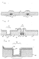
- an integrated circuit device is to be formed in a substrate 10 .
- Gate electrodes 12 are formed over the substrate 10 and spaced therefrom by gate oxide layer 14 .
- Sidewall spacers 16 are formed along side the gate electrodes 12 as known in the art.
- An interlevel insulating layer 18 is formed over the entire surface of the device.
- Interlevel insulating layer 18 can be, for example, a conformally deposited undoped oxide, a reflow glass or spin on glass, or a combination of different insulating layers. Formation of the structures described so far are conventional, and well known in the art.
- Openings 20 and 22 are formed through the interlevel insulating layer 18 . Opening 20 contacts the substrate 10 while opening 22 exposes a portion of the gate electrode 12 .
- those portions of the substrate 10 exposed in the opening 20 are silicided to form a silicided contact region 24 .
- a layer 26 of CVD nitride is then deposited over the surface of the device. This conformal layer 26 fills the sides and bottoms of the openings 20 , 22 , and provides a diffusion barrier for a metal interconnect layer (not shown) to be deposited later over the device.
- a number of process alternatives are provided for by the present invention. These are discussed in more detail in connection with Figure 4 , but generally include the introduction of oxygen into the nitride layer 26 . A small amount of oxygen diffuses into the nitride layer 26 , improving its resistance to the migration of silicon and aluminum atoms during later processing steps.
- the wafer containing the integrated circuit is placed into a sputtering machine.
- a titanium layer 28 is sputtered over the device in an argon atmosphere, preferably to a thickness of approximately 600 angstroms.
- Nitrogen is then introduced into the atmosphere of the sputtering chamber, while deposition of the titanium continues.
- This forms a titanium nitride layer 30 over the surface of the device, preferably to a thickness of approximately 1000 angstroms.
- the device is subjected to a thermal process, preferably a rapid thermal anneal, which forms a silicide region 32 below the opening 20 .
- the entire thickness of the nitride layer 30 is substantially stochiometric (1:1). This provides an improved diffusion barrier when compared with prior art techniques of converting a previously deposited titanium layer to titanium nitride. Deposition of the stochiometric nitride layer also occurs with the alternative arrangement shown in Figure 2 .
- the wafer containing the integrated circuit device is preferably exposed to an atmosphere containing oxygen after formation of either the nitride layer 26 or the nitride layer 30 .
- this can be performed in conjunction with a thermal treatment to enhance the diffusion of oxygen atoms into the nitride layer 26 , 30 .
- the nitride layer was substantially stochiometric, the resulting layer still contains approximately even proportions of titanium and nitrogen, with small amounts of oxygen.
- oxygen can actually be included in the titanium nitride layers 26 and 30 as they are formed.
- the nitrogen is introduced into the atmosphere of the sputtering chamber, small amounts of oxygen may also be introduced. This will cause small amounts of oxygen to be formed directly in the titanium nitride layer 30 , so that a later oxygen diffusion step is not required.
- it remains desirable to perform a thermal anneal of the device in order to form the silicide layer region 32 which improves contact resistance.
- FIG 4 two flow charts are shown which illustrate some of the process steps just described.
- Figure 4(a) illustrates the alternative shown in connection with Figure 3 .
- titanium is sputtered onto the device in argon 40 .
- nitrogen and oxygen are introduced into the atmosphere of the sputtering chamber 42 .
- Sputtering continues 44 , forming a nitride layer having small amounts of oxygen included therein. If desired, the oxygen may be left out when the nitrogen is introduced in step 42 , and diffused into the resulting nitride layer during the later anneal step.
- FIG. 4(b) illustrates several optional steps which can be used to introduce oxygen into the titanium nitride layer as described above.
- the titanium nitride layer is deposited 50 .
- small amounts of oxygen may be deposited with the titanium nitride layer, but this discussion will assume that this was not the case.
- the flow lines of the flow chart of Figure 4(b) may be followed in any combination.
- oxygen may be introduced into the nitride layer in a plasma environment 52 after the formation of the nitride layer 26 or 30 has been completed.
- the wafer containing the device may be moved to a separate chamber in a multichamber machine, and exposed to oxygen in such chamber 54 . Finally, the wafer may be moved to a rapid thermal processor, and subjected to an anneal in an ambient containing nitrogen with small amounts of oxygen.
- the three oxygen diffusion steps 52 , 54 , 56 may be selected and performed in any combination.
- any of them can be performed on a titanium nitride layer 26 , 30 which was formed with oxygen initially available in the ambient atmosphere during sputtering or CVD deposition.
- the oxygen plasma step 52 is typically performed after deposition is complete, and may be performed at a partial pressure of oxygen of approximately 10 ⁇ 5 torr to 10 ⁇ 2 torr , at a temperature of between 100°C and 500°C. If the wafer is moved to a separate chamber (step 54 ), the wafer may be exposed to an atmosphere of oxygen and argon at a temperature of between approximately room temperature and 500°C.
- a thermal anneal step in oxygen 56 is preferably performed in an atmosphere containing nitrogen and oxygen at a temperature in the range of approximately 450° to 750°C.
- formation of the titanium nitride layer according to the described embodiments results in an improved diffusion barrier layer. This is believed to be caused by a stuffing of the grain boundaries of the titanium nitride by oxygen and nitrogen atoms during and after the nitride layer formation. This inhibits the mobility of aluminum and silicon atoms through the nitride layer between grain boundaries.
- a thicker layer of substantially stochiometric titanium nitride is formed than in the case of prior art techniques, and an improved diffusion barrier layer results.
- This improved diffusion barrier minimizes intermingling of aluminum and silicon atoms at contact regions, preventing detrimental side affects of such intermingling as is known in the art.
Landscapes
- Internal Circuitry In Semiconductor Integrated Circuit Devices (AREA)
- Electrodes Of Semiconductors (AREA)
Applications Claiming Priority (2)
| Application Number | Priority Date | Filing Date | Title |
|---|---|---|---|
| US80085591A | 1991-11-26 | 1991-11-26 | |
| US800855 | 1991-11-26 |
Publications (1)
| Publication Number | Publication Date |
|---|---|
| EP0545602A1 true EP0545602A1 (fr) | 1993-06-09 |
Family
ID=25179552
Family Applications (1)
| Application Number | Title | Priority Date | Filing Date |
|---|---|---|---|
| EP92310724A Withdrawn EP0545602A1 (fr) | 1991-11-26 | 1992-11-24 | Procédé de fabrication de couches barrière métalliques |
Country Status (2)
| Country | Link |
|---|---|
| EP (1) | EP0545602A1 (fr) |
| JP (1) | JPH05267211A (fr) |
Cited By (16)
| Publication number | Priority date | Publication date | Assignee | Title |
|---|---|---|---|---|
| EP0551117A3 (fr) * | 1992-01-08 | 1995-06-07 | Mitsubishi Electric Corp | |
| EP0680077A1 (fr) * | 1994-04-29 | 1995-11-02 | STMicroelectronics, Inc. | Circuit intégré avec barrière de contact améliorée |
| GB2290166A (en) * | 1994-06-10 | 1995-12-13 | Samsung Electronics Co Ltd | Wiring structure and method of manufacture |
| GB2291264A (en) * | 1994-07-07 | 1996-01-17 | Hyundai Electronics Ind | Method for forming a metallic barrier layer |
| EP0747500A1 (fr) * | 1995-06-07 | 1996-12-11 | Applied Materials, Inc. | Procédé de fabrication de couches à barrières contenant du titane |
| EP0732731A3 (fr) * | 1995-03-13 | 1997-10-08 | Applied Materials Inc | Traitement d'une couche de nitrure de titane pour améliorer la résistance à des températures élevées |
| US5858184A (en) * | 1995-06-07 | 1999-01-12 | Applied Materials, Inc. | Process for forming improved titanium-containing barrier layers |
| US5895266A (en) * | 1996-02-26 | 1999-04-20 | Applied Materials, Inc. | Titanium nitride barrier layers |
| EP0867941A3 (fr) * | 1997-03-28 | 2000-04-05 | Applied Materials, Inc. | Structure d'interconnexion pour un circuit intégré |
| US6069073A (en) * | 1997-09-18 | 2000-05-30 | Electronics And Telecommunications Research Institute | Method for forming diffusion barrier layers |
| US6155198A (en) * | 1994-11-14 | 2000-12-05 | Applied Materials, Inc. | Apparatus for constructing an oxidized film on a semiconductor wafer |
| US6291343B1 (en) | 1994-11-14 | 2001-09-18 | Applied Materials, Inc. | Plasma annealing of substrates to improve adhesion |
| US6365495B2 (en) | 1994-11-14 | 2002-04-02 | Applied Materials, Inc. | Method for performing metallo-organic chemical vapor deposition of titanium nitride at reduced temperature |
| US6475907B1 (en) * | 1999-04-20 | 2002-11-05 | Nec Corporation | Semiconductor device having a barrier metal layer and method for manufacturing the same |
| US6699530B2 (en) | 1995-07-06 | 2004-03-02 | Applied Materials, Inc. | Method for constructing a film on a semiconductor wafer |
| DE19751785B4 (de) * | 1996-11-22 | 2004-08-05 | Trikon Equipments Ltd., Newport | Verfahren zum Behandeln eines Halbleiter-Wafers |
Families Citing this family (1)
| Publication number | Priority date | Publication date | Assignee | Title |
|---|---|---|---|---|
| KR100187669B1 (ko) * | 1996-01-30 | 1999-06-01 | 김주용 | 반도체 소자의 확산 방지막 형성 방법 |
Citations (4)
| Publication number | Priority date | Publication date | Assignee | Title |
|---|---|---|---|---|
| JPS63164315A (ja) * | 1986-12-26 | 1988-07-07 | Oki Electric Ind Co Ltd | 半導体装置の製造方法 |
| JPH0254926A (ja) * | 1988-08-19 | 1990-02-23 | Seiko Epson Corp | 半導体装置の製造方法 |
| JPH02291124A (ja) * | 1989-04-28 | 1990-11-30 | Fujitsu Ltd | 半導体装置の製造方法 |
| JPH03153077A (ja) * | 1989-11-10 | 1991-07-01 | Seiko Epson Corp | 半導体装置 |
-
1992
- 1992-11-24 EP EP92310724A patent/EP0545602A1/fr not_active Withdrawn
- 1992-11-25 JP JP4315362A patent/JPH05267211A/ja active Pending
Patent Citations (4)
| Publication number | Priority date | Publication date | Assignee | Title |
|---|---|---|---|---|
| JPS63164315A (ja) * | 1986-12-26 | 1988-07-07 | Oki Electric Ind Co Ltd | 半導体装置の製造方法 |
| JPH0254926A (ja) * | 1988-08-19 | 1990-02-23 | Seiko Epson Corp | 半導体装置の製造方法 |
| JPH02291124A (ja) * | 1989-04-28 | 1990-11-30 | Fujitsu Ltd | 半導体装置の製造方法 |
| JPH03153077A (ja) * | 1989-11-10 | 1991-07-01 | Seiko Epson Corp | 半導体装置 |
Non-Patent Citations (4)
| Title |
|---|
| PATENT ABSTRACTS OF JAPAN vol. 012, no. 425 (E-681)10 November 1988 & JP-A-63 164 315 * |
| PATENT ABSTRACTS OF JAPAN vol. 014, no. 222 (E-0926)10 May 1990 & JP-A-02 054 926 ( SEIKO EPSON CORP. ) 23 February 1990 * |
| PATENT ABSTRACTS OF JAPAN vol. 015, no. 070 (E-1035)19 February 1991 & JP-A-02 291 124 ( FUJITSU LTD ) 30 November 1990 * |
| PATENT ABSTRACTS OF JAPAN vol. 015, no. 383 (E-1116)27 September 1991 & JP-A-03 153 077 ( SEIKO EPSON CORP ) 1 July 1991 * |
Cited By (27)
| Publication number | Priority date | Publication date | Assignee | Title |
|---|---|---|---|---|
| EP0551117A3 (fr) * | 1992-01-08 | 1995-06-07 | Mitsubishi Electric Corp | |
| EP0680077A1 (fr) * | 1994-04-29 | 1995-11-02 | STMicroelectronics, Inc. | Circuit intégré avec barrière de contact améliorée |
| US5514908A (en) * | 1994-04-29 | 1996-05-07 | Sgs-Thomson Microelectronics, Inc. | Integrated circuit with a titanium nitride contact barrier having oxygen stuffed grain boundaries |
| US6291344B1 (en) * | 1994-04-29 | 2001-09-18 | Stmicroelectronics, Inc. | Integrated circuit with improved contact barrier |
| US5652464A (en) * | 1994-04-29 | 1997-07-29 | Sgs-Thomson Microelectronics, Inc. | Integrated circuit with a titanium nitride contact barrier having oxygen stuffed grain boundaries |
| US6191033B1 (en) | 1994-04-29 | 2001-02-20 | Stmicroelectronics, Inc. | Method of fabricating an integrated circuit with improved contact barrier |
| US5998870A (en) * | 1994-06-10 | 1999-12-07 | Samsung Electronics Co., Ltd. | Wiring structure of semiconductor device and method for manufacturing the same |
| GB2290166A (en) * | 1994-06-10 | 1995-12-13 | Samsung Electronics Co Ltd | Wiring structure and method of manufacture |
| GB2290166B (en) * | 1994-06-10 | 1998-09-09 | Samsung Electronics Co Ltd | Manufacturing method for a wiring structure of a semiconductor device |
| GB2291264A (en) * | 1994-07-07 | 1996-01-17 | Hyundai Electronics Ind | Method for forming a metallic barrier layer |
| GB2291264B (en) * | 1994-07-07 | 1998-07-29 | Hyundai Electronics Ind | Method for forming a metallic barrier layer in semiconductor device and device made by the method |
| US6155198A (en) * | 1994-11-14 | 2000-12-05 | Applied Materials, Inc. | Apparatus for constructing an oxidized film on a semiconductor wafer |
| US6365495B2 (en) | 1994-11-14 | 2002-04-02 | Applied Materials, Inc. | Method for performing metallo-organic chemical vapor deposition of titanium nitride at reduced temperature |
| US6291343B1 (en) | 1994-11-14 | 2001-09-18 | Applied Materials, Inc. | Plasma annealing of substrates to improve adhesion |
| EP0732731A3 (fr) * | 1995-03-13 | 1997-10-08 | Applied Materials Inc | Traitement d'une couche de nitrure de titane pour améliorer la résistance à des températures élevées |
| US5943600A (en) * | 1995-03-13 | 1999-08-24 | Applied Materials, Inc. | Treatment of a titanium nitride layer to improve resistance to elevated temperatures |
| US6007684A (en) * | 1995-06-07 | 1999-12-28 | Applied Materials, Inc. | Process for forming improved titanium-containing barrier layers |
| US5858184A (en) * | 1995-06-07 | 1999-01-12 | Applied Materials, Inc. | Process for forming improved titanium-containing barrier layers |
| EP0747500A1 (fr) * | 1995-06-07 | 1996-12-11 | Applied Materials, Inc. | Procédé de fabrication de couches à barrières contenant du titane |
| US5972178A (en) * | 1995-06-07 | 1999-10-26 | Applied Materials, Inc. | Continuous process for forming improved titanium nitride barrier layers |
| US6699530B2 (en) | 1995-07-06 | 2004-03-02 | Applied Materials, Inc. | Method for constructing a film on a semiconductor wafer |
| US6238803B1 (en) | 1996-02-26 | 2001-05-29 | Applied Materials, Inc. | Titanium nitride barrier layers |
| US5895266A (en) * | 1996-02-26 | 1999-04-20 | Applied Materials, Inc. | Titanium nitride barrier layers |
| DE19751785B4 (de) * | 1996-11-22 | 2004-08-05 | Trikon Equipments Ltd., Newport | Verfahren zum Behandeln eines Halbleiter-Wafers |
| EP0867941A3 (fr) * | 1997-03-28 | 2000-04-05 | Applied Materials, Inc. | Structure d'interconnexion pour un circuit intégré |
| US6069073A (en) * | 1997-09-18 | 2000-05-30 | Electronics And Telecommunications Research Institute | Method for forming diffusion barrier layers |
| US6475907B1 (en) * | 1999-04-20 | 2002-11-05 | Nec Corporation | Semiconductor device having a barrier metal layer and method for manufacturing the same |
Also Published As
| Publication number | Publication date |
|---|---|
| JPH05267211A (ja) | 1993-10-15 |
Similar Documents
| Publication | Publication Date | Title |
|---|---|---|
| US6903462B2 (en) | Chemical vapor deposition of titanium | |
| JP3132750B2 (ja) | 多層構造、半導体構造、半導体デバイスのコンデンサ、シリコン構造の酸化を防ぐ方法、及び、ドーパントの拡散を防ぐ方法 | |
| US4920073A (en) | Selective silicidation process using a titanium nitride protective layer | |
| US6770571B2 (en) | Barrier in gate stack for improved gate dielectric integrity | |
| US5378660A (en) | Barrier layers and aluminum contacts | |
| US6410427B1 (en) | Metal silicidation methods and methods for using same | |
| US6524953B1 (en) | Asymmetric, double-sided self-aligned silicide and method of forming the same | |
| US5907784A (en) | Method of making multi-layer gate structure with different stoichiometry silicide layers | |
| US5677244A (en) | Method of alloying an interconnect structure with copper | |
| EP0680077B1 (fr) | Circuit intégré avec barrière de contact améliorée | |
| JPH08191054A (ja) | 半導体装置及びその製造方法 | |
| CA2043172C (fr) | Methode et structure pour interconnecter differentes zones de polysiilcium sur des substrats de semiconducteur dans les circuits integres | |
| JPH05267211A (ja) | バリア金属層形成方法 | |
| JP3213909B2 (ja) | 抵抗およびその作製方法 | |
| JPH08264448A (ja) | 緻密なチタン窒化膜及び緻密なチタン窒化膜/薄膜のチタンシリサイドの形成方法及びこれを用いた半導体素子の製造方法 | |
| US5421974A (en) | Integrated circuit having silicide-nitride based multi-layer metallization | |
| US6433434B1 (en) | Apparatus having a titanium alloy layer | |
| US6403458B2 (en) | Method for fabricating local interconnect structure for integrated circuit devices, source structures | |
| US20060202283A1 (en) | Metal silicide adhesion layer for contact structures | |
| US20020175413A1 (en) | Method for utilizing tungsten barrier in contacts to silicide and structure produced therby | |
| KR100209931B1 (ko) | 반도체 소자의 실리사이드 형성방법 | |
| US20010019159A1 (en) | Local interconnect structure for integrated circuit devices, source structure for the same, and method for fabricating the same | |
| JPH0748495B2 (ja) | 半導体装置の製造方法 | |
| JPH09237769A (ja) | 半導体装置の製造方法 | |
| JPH04318925A (ja) | トランジスタおよびその製造方法 |
Legal Events
| Date | Code | Title | Description |
|---|---|---|---|
| PUAI | Public reference made under article 153(3) epc to a published international application that has entered the european phase |
Free format text: ORIGINAL CODE: 0009012 |
|
| AK | Designated contracting states |
Kind code of ref document: A1 Designated state(s): DE FR GB IT |
|
| 18D | Application deemed to be withdrawn |
Effective date: 19940221 |