EP0545801B1 - Dispositif à supraconducteur avec un canal supraconducteur extrêmement mince formé d'un matériau d'oxyde supraconducteur et procédé pour sa fabrication - Google Patents
Dispositif à supraconducteur avec un canal supraconducteur extrêmement mince formé d'un matériau d'oxyde supraconducteur et procédé pour sa fabrication Download PDFInfo
- Publication number
- EP0545801B1 EP0545801B1 EP92403227A EP92403227A EP0545801B1 EP 0545801 B1 EP0545801 B1 EP 0545801B1 EP 92403227 A EP92403227 A EP 92403227A EP 92403227 A EP92403227 A EP 92403227A EP 0545801 B1 EP0545801 B1 EP 0545801B1
- Authority
- EP
- European Patent Office
- Prior art keywords
- superconducting
- drain region
- source region
- channel
- oxide superconductor
- Prior art date
- Legal status (The legal status is an assumption and is not a legal conclusion. Google has not performed a legal analysis and makes no representation as to the accuracy of the status listed.)
- Expired - Lifetime
Links
- 239000002887 superconductor Substances 0.000 title claims description 106
- 238000000034 method Methods 0.000 title claims description 43
- 239000000463 material Substances 0.000 title claims description 24
- 238000004519 manufacturing process Methods 0.000 title claims description 20
- 239000010409 thin film Substances 0.000 claims description 51
- 239000000758 substrate Substances 0.000 claims description 48
- 239000002184 metal Substances 0.000 claims description 14
- 238000005530 etching Methods 0.000 claims description 11
- 150000001875 compounds Chemical class 0.000 claims description 9
- 229910052710 silicon Inorganic materials 0.000 claims description 8
- 239000010703 silicon Substances 0.000 claims description 8
- 239000013078 crystal Substances 0.000 claims description 7
- 229910002480 Cu-O Inorganic materials 0.000 claims description 4
- 229910002370 SrTiO3 Inorganic materials 0.000 claims description 4
- 238000009413 insulation Methods 0.000 claims description 4
- 229910015901 Bi-Sr-Ca-Cu-O Inorganic materials 0.000 claims description 3
- QPLDLSVMHZLSFG-UHFFFAOYSA-N Copper oxide Chemical class [Cu]=O QPLDLSVMHZLSFG-UHFFFAOYSA-N 0.000 claims description 3
- 229910009203 Y-Ba-Cu-O Inorganic materials 0.000 claims description 3
- 229910021420 polycrystalline silicon Inorganic materials 0.000 claims description 3
- 239000000470 constituent Substances 0.000 claims description 2
- 238000010438 heat treatment Methods 0.000 claims description 2
- 238000004544 sputter deposition Methods 0.000 description 15
- 239000012212 insulator Substances 0.000 description 14
- 238000012545 processing Methods 0.000 description 10
- 239000004065 semiconductor Substances 0.000 description 6
- 238000007738 vacuum evaporation Methods 0.000 description 6
- XUIMIQQOPSSXEZ-UHFFFAOYSA-N Silicon Chemical compound [Si] XUIMIQQOPSSXEZ-UHFFFAOYSA-N 0.000 description 5
- 238000001451 molecular beam epitaxy Methods 0.000 description 5
- 230000000694 effects Effects 0.000 description 4
- 229910052581 Si3N4 Inorganic materials 0.000 description 3
- 239000010408 film Substances 0.000 description 3
- 238000010884 ion-beam technique Methods 0.000 description 3
- HQVNEWCFYHHQES-UHFFFAOYSA-N silicon nitride Chemical compound N12[Si]34N5[Si]62N3[Si]51N64 HQVNEWCFYHHQES-UHFFFAOYSA-N 0.000 description 3
- 230000007547 defect Effects 0.000 description 2
- 238000001020 plasma etching Methods 0.000 description 2
- 238000009751 slip forming Methods 0.000 description 2
- 238000000992 sputter etching Methods 0.000 description 2
- 230000002349 favourable effect Effects 0.000 description 1
- 230000005669 field effect Effects 0.000 description 1
- -1 for example Inorganic materials 0.000 description 1
- 238000012986 modification Methods 0.000 description 1
- 230000004048 modification Effects 0.000 description 1
- 238000002128 reflection high energy electron diffraction Methods 0.000 description 1
Images




Classifications
-
- H—ELECTRICITY
- H10—SEMICONDUCTOR DEVICES; ELECTRIC SOLID-STATE DEVICES NOT OTHERWISE PROVIDED FOR
- H10N—ELECTRIC SOLID-STATE DEVICES NOT OTHERWISE PROVIDED FOR
- H10N60/00—Superconducting devices
- H10N60/20—Permanent superconducting devices
- H10N60/205—Permanent superconducting devices having three or more electrodes, e.g. transistor-like structures
- H10N60/207—Field effect devices
-
- Y—GENERAL TAGGING OF NEW TECHNOLOGICAL DEVELOPMENTS; GENERAL TAGGING OF CROSS-SECTIONAL TECHNOLOGIES SPANNING OVER SEVERAL SECTIONS OF THE IPC; TECHNICAL SUBJECTS COVERED BY FORMER USPC CROSS-REFERENCE ART COLLECTIONS [XRACs] AND DIGESTS
- Y10—TECHNICAL SUBJECTS COVERED BY FORMER USPC
- Y10S—TECHNICAL SUBJECTS COVERED BY FORMER USPC CROSS-REFERENCE ART COLLECTIONS [XRACs] AND DIGESTS
- Y10S505/00—Superconductor technology: apparatus, material, process
- Y10S505/70—High TC, above 30 k, superconducting device, article, or structured stock
- Y10S505/701—Coated or thin film device, i.e. active or passive
-
- Y—GENERAL TAGGING OF NEW TECHNOLOGICAL DEVELOPMENTS; GENERAL TAGGING OF CROSS-SECTIONAL TECHNOLOGIES SPANNING OVER SEVERAL SECTIONS OF THE IPC; TECHNICAL SUBJECTS COVERED BY FORMER USPC CROSS-REFERENCE ART COLLECTIONS [XRACs] AND DIGESTS
- Y10—TECHNICAL SUBJECTS COVERED BY FORMER USPC
- Y10S—TECHNICAL SUBJECTS COVERED BY FORMER USPC CROSS-REFERENCE ART COLLECTIONS [XRACs] AND DIGESTS
- Y10S505/00—Superconductor technology: apparatus, material, process
- Y10S505/725—Process of making or treating high tc, above 30 k, superconducting shaped material, article, or device
- Y10S505/728—Etching
Definitions
- the present invention relates to a superconducting device and a method for manufacturing the same, and more specifically to a superconducting device having an extremely the superconducting channel formed of oxide superconductor material, and a method for manufacturing the same.
- Josephson device is one of well-known superconducting devices. However, since Josephson device is a two-terminal device, a logic gate utilizing Josephson devices becomes complicated. Therefore, three-terminal superconducting devices are more practical.
- Typical three-terminal superconducting devices include two types of super-FET (field effect transistor).
- the first type of the super-FET includes a semiconductor channel, and a superconductor source electrode and a superconductor drain electrode which are formed closely to each other on both side of the semiconductor channel.
- a portion of the semiconductor layer between the superconductor source electrode and the superconductor drain electrode has a greatly recessed or undercut rear surface so as to have a reduced thickness.
- a gate electrode is formed through a gate insulator layer on the portion of the recessed or undercut rear surface of the semiconductor layer between the superconductor source electrode and the superconductor drain electrode.
- a superconducting current flows through the semiconductor layer (channel) between the superconductor source electrode and the superconductor drain electrode due to a superconducting proximity effect, and is controlled by an applied gate voltage.
- This type of the super-FET operates at a higher speed with a low power consumption.
- the second type of the super-FET includes a substrate, a channel of a superconductor formed on the substrate, a superconducting source region and a superconducting drain region positioned at the both sides of the superconducting channel, a source electrode and a drain electrode respectively positioned on the superconducting source region and the superconducting drain region, a gate electrode on the superconducting channel, and a gate insulating layer between the superconducting channel and the gate electrode.
- Superconducting current flowing through the superconducting channel of the super-FET is controlled by a voltage applied to a gate above the superconducting channel.
- Both of the super-FETs mentioned above are voltage controlled devices which are capable of isolating output signal from input one and of having a well defined gain.
- the superconductor source electrode and the superconductor drain electrode have to be positioned within a distance of a few times the coherence length of the superconductor materials of the superconductor source electrode and the superconductor drain electrode.
- a distance between the superconductor source electrode and the superconductor drain electrode has to be made less than about a few ten nanometers, if the superconductor source electrode and the superconductor drain electrode are formed of the oxide superconductor material.
- the super-FET having the superconducting channel has a large current capability, and the fine processing which is required to product the first type of the super-FET is not necessary to product this type of super-FET.
- both of the superconducting channel and the gate insulating layer should have an extremely thin thickness.
- the superconducting channel formed of an oxide superconductor material should have a thickness of less than five nanometers, namely about four or five unit-cells and the gate insulating layer should have a thickness more than ten nanometers which is sufficient to prevent a tunnel current.
- the extremely thin superconducting channel of the oxide superconductor has been usually formed directly on a single crystalline insulator substrate such as MgO (100) substrate.
- a single crystalline insulator substrate such as MgO (100) substrate.
- constituent elements of the substrate are diffused into the superconducting channel while the superconducting channel is formed on the substrate. Since the superconducting channel has an extremely thin thickness, the effect of the diffusant is not negligible. Therefore, properties of the superconducting channel is spoiled so that the super-FET can not have high performance.
- the non-superconducting regions are considered to be generated by a bared Cu-O plane at the bottom surface of the oxide superconductor layer which constitutes the superconducting channel.
- the extremely thin superconducting channel is connected to the relatively thick superconducting source region and the superconducting drain region at their lower portions and is far from the source electrode positioned on the superconducting source region and the drain electrodes positioned on the superconducting drain region, the superconducting current flowing through the superconducting channel spreads in the superconducting source region and the superconducting drain region. Therefore, the superconducting current does not flow into nor flow from the superconducting channel, efficiently.
- the European Patent Application N° A1 - 0 478 464 describing the state of the art in accordance with Art. 54(3) EPC discloses a superconducting device comprising a substrate, a projecting insulating region formed on a principal surface of said substrate, and a superconducting channel formed on the projecting insulating region.
- the superconducing channel and the projecting region comprise the same elements, but the projecting region has lost its superconductivity in order to form the weak link which constitutes the superconducting channel.
- an object of the present invention to provide an FET type superconducting device having a superconducting channel constituted of an extremely thin oxide superconductor film, which have overcome the above mentioned defects of the conventional ones.
- Another object of the present invention is to provide a method for manufacturing an FET type superconducting device which have overcome the above mentioned defects of the conventional ones.
- the superconducting channel of the superconducting device in accordance with the present invention is connected to the superconducting source region and the superconducting drain region at the higher portions than their one third height portions, superconducting current does not spread in the superconducting source region and the superconducting drain region. Therefore, the superconducting current efficiently flows into or flows from the superconducting channel.
- the superconducting source region and the superconducting drain region of the superconducting device in accordance with the present invention have a thickness of 100 to 500 nanometers and a non-superconducting layer interposed between the substrate and the channel layer preferably has a thickness ranging one third of the thickness of the superconducting source region and the superconducting drain region to the same thickness.
- the non-superconducting layer has a thickness which is approximately half that of the superconducting source region and the superconducting drain region.
- the superconducting channel is preferably connected to middle portions of the superconducting source region and the superconducting drain region.
- the gate insulating layer also covers the side surfaces of the superconducting source region and the superconducting drain region so as to isolate the gate electrode from the superconducting source region and the superconducting drain region.
- opposite side surfaces of the superconducting source region and the superconducting drain region are slanted so that a vacancy between the superconducting source region and the superconducting drain region has a shape of a trapezoid, the superconducting source region and the superconducting drain region become shorter at the lower portions and the shortest at the bottom, and the non-superconducting layer is longer than the gate insulating layer, which is longer than the gate electrode.
- the gate electrode does not contact with the superconducting source region and the superconducting drain region.
- the slant side surfaces contribute to the improvement of the efficiency of the superconducting current flow.
- the gate electrode is formed of a material which includes silicon, for example, polycrystalline silicon.
- the gate electrode is isolated from the superconducting source region and the superconducting drain region by insulation regions which are formed by silicon diffused from the gate electrode into the superconducting source region and the superconducting drain region. It is preferable that the superconducting device further includes a metal layer on the gate insulating layer which prevent silicon from diffusing into the superconducting channel.
- the non-superconducting layer has almost same thickness as those of the superconducting source region and the superconducting drain region.
- the superconducting channel is preferably connected to top portions of the superconducting source region and the superconducting drain region.
- the superconducting channel of this superconducting device is constituted of an extremely thin oxide superconductor film which is deposited on the planar surfaces of the non-superconducting layer, the superconducting source region and the superconducting drain region. Therefore, the oxide superconductor thin film is free from stress so that the properties of the superconducting channel is improved.
- the non-superconducting layer can be formed of an insulator material which does not react with the oxide superconductor and does not diffuse into the oxide superconductor thin film, such as MgO, SrTiO 3 , etc.
- the non-superconducting layer is preferably formed of an oxide of which the crystal structure is similar to that of the oxide superconductor such as Pr 1 Ba 2 Cu 3 O 7- ⁇ .
- Pr 1 Ba 2 Cu 3 O 7- ⁇ compensate for crystalline incompleteness of an oxide superconductor thin film so that properties of the oxide superconductor thin film is improved.
- the oxide layer formed of a c -axis orientated Pr 1 Ba 2 Cu 3 O 7- ⁇ thin film is favorable. Since the c -axis orientated Pr 1 Ba 2 Cu 3 O 7- ⁇ thin film has an almost same crystal lattice structure as that of a c -axis orientated oxide superconductor thin film.
- cross-sectional area of the superconducting channel of the superconducting device in accordance with the present invention is the same size as desired and substantially larger than that of a conventional superconducting device.
- the superconducting device in accordance with the present invention has a larger current capability than a conventional one.
- the oxide superconductor is formed of high-T c (high critical temperature) oxide superconductor, particularly, formed of a high-T c copper-oxide type compound oxide superconductor for example a Y-Ba-Cu-O compound oxide superconductor material, a Bi-Sr-Ca-Cu-O compound oxide superconductor material, and a Tl-Ba-Ca-Cu-O compound superconductor material.
- high-T c high critical temperature oxide
- a high-T c copper-oxide type compound oxide superconductor for example a Y-Ba-Cu-O compound oxide superconductor material, a Bi-Sr-Ca-Cu-O compound oxide superconductor material, and a Tl-Ba-Ca-Cu-O compound superconductor material.
- the gate insulating layer can be formed of an insulator material, preferably formed of SrTiO 3 , MgO, SiN, etc.
- the substrate can be formed of an insulating substrate, preferably an oxide single crystalline substrate such as MgO, SrTiO 3 , CdNdAlO 4 , etc. These substrate materials are very effective in forming or growing a crystalline film having a high degree of crystalline orientation.
- the superconducting channel is formed of a c -axis orientated oxide superconductor thin film.
- the non-superconducting layer is formed so as to have an approximately half thickness of the first oxide superconductor thin film.
- the non-superconducting layer, the superconducting channel, the gate insulating layer and the gate electrode are formed on the exposed surface of the substrate between the superconducting source region and the superconducting drain region. In other words, they are formed at the hollow portion between the superconducting source region and the superconducting drain region. Therefore, the superconducting channel, the gate insulating layer and the gate electrode can be self-aligned.
- the gate insulating layer is preferably formed so as to cover the side surfaces of the superconducting source region and the superconducting drain region.
- first oxide superconductor thin film is preferably etched by an isotropic etching process so as to form a vacancy having a shape of a trapezoid between the superconducting source region and the superconducting drain region, the superconducting source region and the superconducting drain region become shorter at the lower portions and the shortest at the bottom.
- the non-superconducting layer is formed so as to have almost the same thickness as those of the superconducting source region and the superconducting drain region.
- the method in accordance with the present invention further includes a step of heating the substrate to a temperature of 350 to 400 °C under a pressure lower than 1.333 ⁇ 10 -7 Pa (1 ⁇ 10 -9 Torr) after etching the first oxide superconductor thin film in order to clean the exposed surface of the substrate.
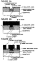
- a MgO (100) single crystalline substrate 5 having a substantially planar principal surface ((100) surface) is prepared.
- a c -axis orientated Y 1 Ba 2 Cu 3 O 7- ⁇ oxide superconductor thin film 11 having a thickness of about 250 nanometers is deposited on a principal surface of a MgO substrate 5, by for example a sputtering, an MBE (molecular beam epitaxy), a vacuum evaporation, a CVD, etc.
- a condition of forming the c -axis orientated Y 1 Ba 2 Cu 3 O 7- ⁇ oxide superconductor thin film 11 by off-axis sputtering is as follows: Temperature of the substrate 700°C Sputtering Gas Ar: 90% O 2 : 10% Pressure 6.665 Pa (5 ⁇ 10 -2 Torr)
- a center portion of the Y 1 Ba 2 Cu 3 O 7- ⁇ oxide superconductor thin film 11 is selectively etched by a reactive ion etching process using a chloric gas, an ion milling using Ar-ions or a focused ion beam etching, so that the oxide superconductor of the portion 14 is completely removed and a superconducting source region 2 and a superconducting drain region 3 are formed separately on the substrate 5, as shown in Figure 1C. A surface of the substrate 5 is exposed at the portion 14.
- an oxide layer 15 having a thickness of 150 nanometers composed of c -axis orientated Pr 1 Ba 2 Cu 3 O 7- ⁇ is deposited on the exposed surface 14 of the substrate 5, by an MBE.
- the oxide layer 15 preferably has a thickness ranging from one third to the same thickness of the superconducting source region 2 and the superconducting drain region 3.
- Pr 1 Ba 2 Cu 3 O 7- ⁇ thin film 15 While the Pr 1 Ba 2 Cu 3 O 7- ⁇ thin film 15 is growing, the surface morphology of the Pr 1 Ba 2 Cu 3 O 7- ⁇ thin film 15 is monitored by RHEED.
- a condition of forming the c -axis orientated Pr 1 Ba 2 Cu 3 O 7- ⁇ oxide thin film 15 by MBE is as follows: Molecular beam source Pr: 1225°C Ba: 600°C Cu: 1040°C Pressure 1.333 ⁇ 10 -3 Pa (1 ⁇ 10 -5 Torr) Temperature of the substrate 700°C
- the Pr molecular beam source is exchanged to a Y molecular beam source so that a superconducting channel 10 of a c -axis orientated Y 1 Ba 2 Cu 3 O 7- ⁇ oxide superconductor thin film having a thickness of about 5 nanometer is continuously formed on the oxide layer 15 of Pr 1 Ba 2 Cu 3 O 7- ⁇ thin film, as shown in Figure 1E.
- the Pr 1 Ba 2 Cu 3 O 7- ⁇ oxide thin film and Y 1 Ba 2 Cu 3 O 7- ⁇ oxide superconductor thin film deposited on the superconducting source region 2 and the superconducting drain region 3 can be removed, if necessary.
- an insulator layer 17 of MgO is formed by a sputtering successively on the superconducting source region 2, the superconducting channel 10 and the superconducting drain region 3.
- the insulating layer 17 has a thickness of 10 to 20 nanometers and covers side surfaces of the superconducting source region 2 and the superconducting drain region 3 for their insulation.
- a gate electrode 4 of Au is formed on a center portion of the insulator layer 17 by a vacuum evaporation.
- the center portion of the insulator layer 17 under the gate electrode 4 becomes a gate insulating layer 7.
- a metal source electrode and a metal drain electrode may be formed on the superconducting source region 2 and the superconducting drain region 3 respectively, if necessary. With this, the super-FET in accordance with the present invention is completed.
- the above mentioned super-FET manufactured in accordance with the first embodiment of the method of the present invention has a superconducting channel which is formed on the Pr 1 Ba 2 Cu 3 O 7- ⁇ non-superconducting oxide layer of which the crystal structure is similar to that of the Y 1 Ba 2 Cu 3 O 7- ⁇ oxide superconductor. Therefore, the bottom portion of the superconducting channel is not degraded so that the substantial cross-sectional area of the superconducting channel of the super-FET is larger than that of a conventional super-FET.
- the superconducting channel is connected to the superconducting source region and the superconducting drain region at their middle portions, superconducting current efficiently flows into and flows from the superconducting channel. By all of these, the current capability of the super-FET can be improved.
- the oxide layer, the superconducting channel, the gate insulating layer and the gate electrode are self-aligned. Therefore, the limitation in the fine processing technique required for manufacturing the super-FET is relaxed.
- the oxide superconductor thin film 11 is an a -axis orientated Y 1 Ba 2 Cu 3 O 7- ⁇ oxide superconductor thin film and the oxide layer 15 has a thickness of 100 nanometers.
- the oxide layer 15 of Pr 1 Ba 2 Cu 3 O 7- ⁇ and the superconducting channel 10 of Y 1 Ba 2 Cu 3 O 7- ⁇ oxide superconductor are formed, the oxide layers and the oxide superconductor layers deposited on the superconducting source region 2 and the superconducting drain region 3 are removed.
- a condition of forming the a -axis orientated Y 1 Ba 2 Cu 3 O 7- ⁇ oxide superconductor thin film 11 by off-axis sputtering is as follows: Temperature of the substrate 630°C Sputtering Gas Ar: 90% O 2 : 10% Pressure 6.665 Pa (5 ⁇ 10 -2 Torr)
- an insulator layer 17 of a silicon nitride or MgO is formed by a sputtering successively on the superconducting source region 2, the superconducting channel 10 and the superconducting drain region 3.
- the insulating layer 17 has a thickness of 10 to 20 nanometers and covers side surfaces of the superconducting source region 2 and the superconducting drain region 3 for their insulation.
- an Au layer 24 which will be a gate electrode is formed on the insulator layer 17 by a vacuum evaporation.
- the Au layer 24 is processed into a gate electrode 4, and portions of the insulator layer 17 on the superconducting source region 2 and the superconducting drain region 3 are removed so that a metal source electrode 12 and a metal drain electrode 13 of Au are formed on the superconducting source region 2 and the superconducting drain region 3 respectively.
- the center portion of the insulator layer 17 under the gate electrode 4 becomes a gate insulating layer 7.
- the abovementioned super-FET manufactured in accordance with the second embodiment of the method of the present invention has the superconducting source region 2 and the superconducting drain region 3 formed of a -axis orientated oxide superconductor thin films and the superconducting channel 10 formed of a c -axis orientated oxide superconductor thin film. Therefore, the super-FET has a large current capability.
- the superconducting channel is formed on the Pr 1 Ba 2 Cu 3 O 7- ⁇ non-superconducting oxide layer of which the crystal structure is similar to that the Y 1 Ba 2 Cu 3 O 7- ⁇ oxide superconductor.
- the bottom portion of the superconducting channel is not degraded so that the substantial cross-sectional area of the superconducting channel of the super-FET is larger than that of a conventional super-FET. Additionally, since the superconducting channel is connected to the superconducting source region and the superconducting drain region at their middle portions, superconducting current efficiently flows into and flows from the superconducting channel. By all of these, the current-voltage characteristic of the super-FET can be improved.
- the oxide layer, the superconducting channel, the gate insulating layer and the gate electrode are self-aligned. Therefore, the limitation in the fine processing technique required for manufacturing the super-FET is relaxed.
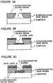
- a center portion of the c -axis orientated Y 1 Ba 2 Cu 3 O 7- ⁇ oxide superconductor thin film 11 is selectively etched by a reactive ion etching process using a chloric gas, an ion milling using Ar-ions or a focused ion beam etching, so that the oxide superconductor of the portion 14 is completely removed and a superconducting source region 2 and a superconducting drain region 3 are formed separately on the substrate 5.
- the portion 14 is side-etched by an isotropic etching process so as to form a vacancy having a shape of a trapezoid.
- the superconducting source region 2 and the superconducting drain region 3 become shorter at the lower portions and the shortest at the bottom.
- a surface of the substrate 5 is exposed at the portion 14.
- the slant side surfaces of the superconducting source region 2 and the superconducting drain region 3 improve efficiency of the superconducting current flow into and from the superconducting channel.
- the vacancy of the portion 14 prevents a gate electrode which will be formed at the portion 14 from contacting the superconducting source region 2 and the superconducting drain region 3, too.
- the substrate is 5 heated to a temperature of 350 to 400 °C under a pressure lower than 1.333 ⁇ 10 -7 Pa (1 ⁇ 10 -9 torr) so as to clean the exposed surface portion 14 of the substrate 5.
- an oxide layer 15 composed of c -axis orientated Pr 1 Ba 2 Cu 3 O 7- ⁇ thin film having a thickness of 150 nanometers is deposited on the exposed surface 14 of the substrate 5, by a sputtering.
- the oxide layer 15 preferably has a thickness ranging from one third to the same thickness of the superconducting source region 2 and the superconducting drain region 3.
- a condition of forming the c -axis orientated Pr 1 Ba 2 Cu 3 O 7- ⁇ oxide thin film 15 by a sputtering is follows: Temperature of the substrate 700°C Sputtering Gas Ar: 90% O 2 : 10% Pressure 6.665 Pa (5 ⁇ 10 -2 Torr)
- a superconducting channel 10 of a c -axis orientated Y 1 Ba 2 Cu 3 O 7- ⁇ oxide superconductor thin film having a thickness of about 5 nanometer is continuously formed by a sputtering on the oxide layer 15 of Pr 1 Ba 2 Cu 3 O 7- ⁇ thin film, as shown in Figure 3C.
- a condition of forming the c -axis orientated Y 1 Ba 2 Cu 3 O 7- ⁇ oxide superconductor thin film is the same as that of the Pr 1 Ba 2 Cu 3 O 7- ⁇ thin film.
- the Pr 1 Ba 2 Cu 3 O 7- ⁇ thin film and Y 1 Ba 2 Cu 3 O 7- ⁇ oxide super conductor thin film deposited on the superconducting source region 2 and the superconducting drain region 3 can be removed, if necessary.
- a gate insulating layer 7 of MgO is formed by a sputtering or a CVD on the superconducting channel 10.
- the gate insulating layer 7 has a thickness of 10 to 20 nanometers.
- a gate electrode 4 of Au is formed on a center portion of the gate insulating layer 7 by a vacuum evaporation apart from the superconducting source region 2 and the superconducting drain region 3.
- a metal source electrode and a metal drain electrode may be formed on the superconducting source region 2 and the superconducting drain region 3 respectively, if necessary.
- the above mentioned super-FET manufactured in accordance with the third embodiment of the method of the present invention has a superconducting channel which is formed on the Pr 1 Ba 2 Cu 3 O 7- ⁇ non-superconducting oxide layer of which the crystal structure is similar to that of the Y 1 Ba 2 Cu 3 O 7- ⁇ oxide superconductor. Therefore, the bottom portion of the superconducting channel is not degraded so that the substantial cross-sectional area of the superconducting channel of the super-FET is larger than that of a conventional super-FET.
- the superconducting source region and the superconducting drain region have slant side surfaces and the superconducting channel is connected to the superconducting source region and the superconducting drain region at middle portions of slant surfaces, superconducting current efficiently flows into and flows from the superconducting channel. By these, the current capability of the super-FET can be improved. In the above mentioned process, the super-FET can be manufactured only by sputtering and CVD which are simpler than MBE.
- the oxide layer, the superconducting channel, the gate insulating layer and the gate electrode are self-aligned. Therefore, the limitation in the fine processing technique required for manufacturing the super-FET is relaxed.
- the oxide superconductor thin film 11 is an a -axis orientated Y 1 Ba 2 Cu 3 O 7- ⁇ oxide superconductor thin film and the oxide layer 15 has a thickness of 100 nanometers.
- the oxide layer 15 of Pr 1 Ba 2 Cu 3 O 7- ⁇ and the superconducting channel 10 of Y 1 Ba 2 Cu 3 O 7- ⁇ oxide superconductor are formed, the oxide layers and the oxide superconductor layers deposited on the superconducting source region 2 and the superconducting drain region 3 are removed, if necessary.
- a gate insulating layer 7 of a silicon nitride or MgO is formed by a sputtering on the superconducting channel 10.
- the gate insulating layer 7 has a thickness of 10 to 20 nanometers.
- a Pt layer 41 is formed on the gate insulating layer 7 by a vacuum evaporation and a gate electrode 4 is formed of polycrystalline silicon on the Pt layer 41.
- the substrate 5 is heated to a temperature of 800 °C so that silicon is diffused into the superconducting source region and the superconducting drain region so as to form a insulating region 50, as shown in Figure 4C.
- the Pt layer 41 prevents silicon from diffusing into the superconducting channel 10. Portions of the stacked layers on the superconducting source region 2 and the superconducting drain region 3 are removed so that a metal source electrode 12 and metal drain electrode 13 of Au are formed on the superconducting source region 2 and the superconducting drain region 3 respectively. With this, the super-FET in accordance with the present invention is completed.
- the above mentioned super-FET manufactured in accordance with the fourth embodiment of the method of the present invention has the superconducting channel which is formed on the Pr 1 Ba 2 Cu 3 O 7- ⁇ non-superconducting oxide layer of which the crystal structure is similar to that of the Y 1 Ba 2 Cu 3 O 7- ⁇ oxide superconductor. Therefore, the bottom portion of the superconducting channel is not degraded so that the substantial cross-sectional area of the superconducting channel of the super-FET is larger than that of a conventional super-FET. Additionally, since the superconducting channel is connected to the superconducting source region and the superconducting drain region at their middle portions, superconducting current efficiently flows into and flows from the superconducting channel.
- the current-voltage characteristic of the super-FET can be improved.
- the non-superconducting oxide layer 15, the superconducting channel 10, the gate insulating layer 7 and the gate electrode 4 are self-aligned and the insulating region 50 which isolates the gate electrode 4 from the superconducting source region 2 and the superconducting drain region 3 is also made self-align manner.
- an insulating region 150 of Pr 1 Ba 2 Cu 3 O 7- ⁇ is formed between the superconducting source region 2 and the superconducting drain region 3 so as to have almost the same thickness as those of the superconducting source region 2 and the superconducting drain region 3.
- upper surface of the insulating region 150 is the same level as those of he superconducting source region 2 and the superconducting drain region 3, and the upper surfaces are successive and planar.
- the insulating region 150 is formed by a CVD and then needless portion of the formed insulating region is removed by a lift-off process or a focused ion beam etching process.
- the upper surfaces of the insulating region 150, the superconducting source region 2 and the superconducting drain region 3 may be etched back, if necessary.
- a Y 1 Ba 2 Cu 3 O 7- ⁇ oxide superconductor thin film 21 having a thickness of 5 nanometers and a insulator layer 17 having a thickness of about 10 nanometers of MgO or silicon nitride are formed by successive sputtering processes.
- the portion of the Y 1 Ba 2 Cu 3 O 7- ⁇ oxide superconductor thin film 21 on the insulating region 50 will be a superconducting channel, when the super-FET will be completed.
- an Au layer 24 is formed on the insulator layer 17 by a vacuum evaporation.
- the Au layer 24 is processed into a gate electrode 4 and the insulator layer 17 is processed into a gate insulating layer 7, which are arranged on the insulating region 150, as shown in Figure 5D.
- a metal source electrode and a metal drain electrode may be formed on the superconducting source region 2 and the superconducting drain region 3 respectively, if necessary. With this, the super-FET in accordance with the present invention is completed.
- the above mentioned super-FET manufactured in accordance with the fifth embodiment of the method of the present invention has a superconducting channel which is formed of the oxide superconductor thin film on the planar surfaces of the insulating region 150, the superconducting source region 2 and the superconducting drain region 3. Therefore, the superconducting channel 10 is free from a stress so as to have good properties. Additionally, since the position and the length of the superconducting channel 10 are determined by the insulating region 150, the dimensions of the superconducting device, especially the length of the superconducting channel 10 can be accurately determined.
- the superconducting channel 10 is connected to the top portions of the superconducting source region 2 and the superconducting drain region 3, superconducting current does not spreads in the superconducting source region 2 and the superconducting drain region 3. Therefore, the superconducting current flows into and flow from the superconducting channel, efficiently.
- the oxide superconductor thin film can be formed of not only Y-Ba-Cu-O compound oxide superconductor material, but also a high-T c (high critical temperature) oxide superconductor material, particularly a high-T c copper-oxide type compound oxide superconductor material, for example a Bi-Sr-Ca-Cu-O compound oxide superconductor material, and a Tl-Ba-Ca-Cu-O compound oxide superconductor material.
- a high-T c oxide superconductor material particularly a high-T c copper-oxide type compound oxide superconductor material, for example a Bi-Sr-Ca-Cu-O compound oxide superconductor material, and a Tl-Ba-Ca-Cu-O compound oxide superconductor material.
Landscapes
- Superconductor Devices And Manufacturing Methods Thereof (AREA)
Claims (25)
- Dispositif supraconducteur comprenant un substrat (5); une couche non-supraconductrice (15, 150), formée sur une surface principale dudit substrat; un canal supraconducteur (10) formé d'une couche mince d'oxyde supraconducteur sur ladite couche non-supraconductrice ; une zone de source supraconductrice (2) et une zone de drain supraconductrice (3) formées d'une autre couche dudit oxyde supraconducteur bien plus épaisse que le canal supraconducteur (10), des deux côtés du canal supraconducteur (10), séparées l'une de l'autre mais connectées électriquement à travers le canal supraconducteur, de sorte qu'un courant supraconducteur peut circuler à travers le canal supraconducteur (10) entre la zone de source supraconductrice (2) et la zone de drain supraconductrice (3) ; et une électrode de grille (4) située au-dessus d'une couche isolante de grille (7) présente sur le canal supraconducteur (10) pour commander le courant supraconducteur circulant dans le canal supraconducteur ; ladite couche non-supraconductrice (15, 150) étant formée d'un oxyde possédant une structure cristalline semblable à celle dudit oxyde supraconducteur de telle sorte qu'il compense l'imperfection cristalline du film mince d'oxyde supraconducteur , améliorant de ce fait la capacité de courant du canal supraconducteur entre la surface principale du substrat(5) et le canal supraconducteur (10);
l'oxyde de la couche non-supraconductrice (15, 150) comportant au moins un élément constituant qui n'est pas inclus dans l'oxyde supraconducteur et la surface inférieure du canal supraconducteur (10) étant connectée aux parties de la zone de source supraconductrice (2) et de la zone de drain supraconductrice (3), lesquelles parties sont situées entre un tiers de la hauteur de la zone de source supraconductrice et de la zone de drain supraconductrice et la hauteur totale de celles-ci. - Dispositif supraconducteur selon la revendication 1 , caractérisé en ce que l'épaisseur de ladite couche non-supraconductrice (15, 150) correspond approximativement à la moitié de l'épaisseur de la zone de source supraconductrice (2) et de la zone de drain supraconductrice (3).
- Dispositif supraconducteur selon la revendication 1 ou 2 , caractérisé en ce que le canal supraconducteur (10) est connecté aux parties de la zone de source supraconductrice (2) et de la zone de drain supraconductrice (3) au niveau approximatif de la moitié de l'épaisseur de ces zones.
- Dispositif supraconducteur selon l'une quelconque des revendications 1 à 3, caractérisé en ce que la couche isolante de grille (7) recouvre également les surfaces latérales de la zone de source supraconductrice (2)et de la zone de drain supraconductrice (3) de façon à isoler l'électrode de grille (4) de la zone de source supraconductrice et de la zone de drain supraconductrice.
- Dispositif supraconducteur selon l'une quelconque des revendications 1 à 3, caractérisé en ce que les surfaces latérales opposées de la zone de source supraconductrice (2) et de la zone de drain supraconductrice (3) sont inclinées de sorte qu'un espace (14) situé entre la zone de source supraconductrice et la zone de drain supraconductrice présente une forme trapézoïdale, la zone de source supraconductrice (2) et la zone de drain supraconductrice (3) deviennent plus courtes au niveau des parties inférieures et les plus courtes au niveau de la base, et la couche non-supraconductrice (15) est plus longue que la couche isolante de grille (7) qui est plus longue que l'électrode de grille (4).
- Dispositif supraconducteur selon l'une quelconque des revendications 1 à 3, caractérisé en ce que l'électrode de grille (4) est constituée d'un matériau qui inclut du silicium.
- Dispositif supraconducteur selon la revendication 6 , caractérisé en ce que l'électrode de grille (4) est formée de silicium polycristallin.
- Dispositif supraconducteur selon la revendication 6 ou 7, caractérisé en ce que l'électrode de grille (4) est isolée de la zone de source supraconductrice (2) et de la zone de drain supraconductrice (3) par une zone isolante (50) qui est formée de silicium ayant diffusé à partir de l'électrode de grille dans la zone de source supraconductrice et dans la zone de drain supraconductrice.
- Dispositif supraconducteur selon la revendication 8, caractérisé en ce que le dispositif supraconducteur comprend , de plus, une couche métallique sur la couche isolante de grille qui empêche le silicium de diffuser dans le canal supraconducteur.
- Dispositif supraconducteur selon l'une quelconque des revendications 1 à 9, caractérisé en ce que la couche non-supraconductrice (15, 150) présente pratiquement la même épaisseur que 1' épaisseur de la zone de source supraconductrice (2) et la zone de drain supraconductrice (3).
- Dispositif supraconducteur selon la revendication 10, caractérisé en ce que le canal supraconducteur (10) est connecté aux parties supérieures de la zone de source supraconductrice (2) et de la zone de drain supraconductrice (3).
- Dispositif supraconducteur selon l'une quelconque des revendications 1 à 11, caractérisé en ce que la couche non-supraconductrice (15, 150) est formée de Pr1Ba2Cu3O7-ε.
- Dispositif supraconducteur selon l'une quelconque des revendications 1 à 12, caractérisé en ce que le dispositif comprend, de plus, une électrode métallique de source (12) située sur la zone de source supraconductrice (2) et une électrode métallique de drain (13) située sur la zone de drain supraconductrice (3).
- Dispositif supraconducteur selon l'une quelconque des revendications 1 à 13, caractérisé en ce que l'oxyde supraconducteur est formé d'un oxyde supraconducteur à Tc élevée (température critique élevée).
- Dispositif supraconducteur selon la revendication 14, caractérisé en ce que l'oxyde supraconducteur est formé d'un supraconducteur d'oxyde composé du type oxyde de cuivre à Tc élevée.
- Dispositif supraconducteur selon la revendication 15 , caractérisé en ce que l'oxyde supraconducteur est formé d'un matériau d'oxyde supraconducteur sélectionné à partir du groupe constitué d'un matériau supraconducteur d'oxyde composé de type Y-Ba-Cu-O , d'un matériau supraconducteur d'oxyde composé de type Bi-Sr-Ca-Cu-O et d'un matériau supraconducteur d'oxyde composé de type Tl-Ba-Ca-Cu-O.
- Dispositif supraconducteur selon l'une quelconque des revendications 1 à 16, caractérisé en ce que le substrat est formé d'un matériau sélectionné à partir du groupe constitué d'un substrat de MgO(100), d'un substrat de SrTiO3 (100) et d'un substrat de CdNdAlO4(001).
- Dispositif supraconducteur selon l'une quelconque des revendications 1 à 17, caractérisé en ce que le canal supraconducteur présente une épaisseur d'environ cinq manomètres , ou moins.
- Dispositif supraconducteur selon l'une quelconque des revendications 1 à 18, caractérisé en ce que la zone de source supraconductrice et la zone de drain supraconductrice présentent chacune une épaisseur de 100 à 500 manomètres.
- Procédé de fabrication d'un dispositif supraconducteur comprenant un substrat (5) présentant une surface principale , une couche non-supraconductrice (15/150) constituée d'un oxyde sur la surface principale du substrat , un canal supraconducteur (10) formé d'un oxyde supraconducteur sur la couche non-supraconductrice (15, 150), une zone de source supraconductrice (2) et une zone de drain supraconductrice (3) constituées dudit oxyde supraconducteur au niveau des deux côtés du canal supraconducteur (10), séparées l'une de l'autre mais connectées électriquement par le canal supraconducteur, de sorte qu'un courant supraconducteur peut circuler à travers le canal supraconducteur (10) entre la zone de source supraconductrice (2) et la zone de drain supraconductrice (3) ; et une électrode de grille (4) située au-dessus d'une couche isolante de grille (7) sur le canal supraconducteur (10) pour commander le courant supraconducteur circulant à travers le canal supraconducteur ;
le procédé comprenant les étapes consistant àformer sur la surface principale du substrat (5) un premier film mince d'oxyde supraconducteur (11) présentant une épaisseur suffisante pour la zone de source supraconductrice (2) et la zone de drain supraconductrice (3) ;graver sélectivement une partie centrale du premier film mince d'oxyde supraconducteur (11) de façon que la partie du premier film mince d'oxyde supraconducteur soit complètement éliminée et une surface du substrat soit exposée de façon à former la zone de source supraconductrice (2) et la zone de drain supraconductrice (3), séparément, sur la surface principale du substrat (5) ;former une couche non-supraconductrice (15, 150) d'un oxyde présentant une épaisseur se situant entre un tiers de l'épaisseur de la zone de source supraconductrice (2) et de la zone de drain supraconductrice (3) et la même épaisseur sur la surface exposée du substrat (5) ;former un second film mince d'oxyde supraconducteur sur la couche non-supraconductrice (15, 150) de façon qu'un canal supraconducteur (10) dont la surface inférieure est connectée aux parties de la zone de source supraconductrice (2) et de la zone de drain supraconductrice (3), en étant placée entre un tiers de la hauteur de la zone de source supraconductrice et de la zone de drain supraconductrice et sa hauteur totale ; etformer une couche isolante de grille (7) sur le canal supraconducteur (10) et une électrode de grille (4) sur la couche isolante de grille (7). - Procédé selon la revendication 20, caractérisé en ce que la couche non-supraconductrice (15) est formée de façon à présenter une épaisseur qui est approximativement la moitié de celle du premier film mince d'oxyde supraconducteur (11) de sorte que le canal supraconducteur (10), la couche isolante de grille (7) et l'électrode de grille (4) puissent être auto-alignés.
- Procédé selon la revendication 20 ou 21 , caractérisé en ce que la couche isolante de grille (7) est formée de façon à recouvrir les surfaces latérales de la zone de source supraconductrice (2) et de la zone de drain supraconductrice (3).
- Procédé selon la revendication 20 , caractérisé en ce que la couche non-supraconductrice (15, 150) est formée de façon à présenter pratiquement la même épaisseur que celle de la zone de source supraconductrice (2) et de la zone de drain supraconductrice (3).
- Procédé selon la revendication 20, caractérisé en ce que le premier film mince d'oxyde supraconducteur (11) est gravé par un procédé de gravure isotrope de façon à former un espace (14) présentant une forme trapézoïdale entre la zone de source supraconductrice (2) et la zone de drain supraconductrice (3), et la zone de source supraconductrice (2) et la zone de drain supraconductrice (3) deviennent plus courtes au niveau des parties inférieures et les plus courtes au niveau de la base.
- Procédé selon l'une quelconque des revendications 20 à 24, caractérisé en ce que le procédé inclut, de plus, une étape de chauffage du substrat à une température de 350 à 400°C sous une pression inférieure à 1,333 x 10-7 Pa (1 x 10⁻⁹ Torr) après gravure du premier film mince d'oxyde supraconducteur (11) afin de nettoyer la surface exposée du substrat (5).
Applications Claiming Priority (8)
| Application Number | Priority Date | Filing Date | Title |
|---|---|---|---|
| JP342468/91 | 1991-11-30 | ||
| JP3342470A JP2680960B2 (ja) | 1991-11-30 | 1991-11-30 | 超電導電界効果型素子およびその作製方法 |
| JP3342467A JP2773503B2 (ja) | 1991-11-30 | 1991-11-30 | 超電導電界効果型素子およびその作製方法 |
| JP3342469A JP2737499B2 (ja) | 1991-11-30 | 1991-11-30 | 超電導電界効果型素子およびその作製方法 |
| JP342469/91 | 1991-11-30 | ||
| JP342470/91 | 1991-11-30 | ||
| JP3342468A JP2680959B2 (ja) | 1991-11-30 | 1991-11-30 | 超電導電界効果型素子およびその作製方法 |
| JP342467/91 | 1991-11-30 |
Publications (2)
| Publication Number | Publication Date |
|---|---|
| EP0545801A1 EP0545801A1 (fr) | 1993-06-09 |
| EP0545801B1 true EP0545801B1 (fr) | 1997-03-19 |
Family
ID=27480617
Family Applications (1)
| Application Number | Title | Priority Date | Filing Date |
|---|---|---|---|
| EP92403227A Expired - Lifetime EP0545801B1 (fr) | 1991-11-30 | 1992-11-30 | Dispositif à supraconducteur avec un canal supraconducteur extrêmement mince formé d'un matériau d'oxyde supraconducteur et procédé pour sa fabrication |
Country Status (4)
| Country | Link |
|---|---|
| US (2) | US5399546A (fr) |
| EP (1) | EP0545801B1 (fr) |
| CA (1) | CA2084174C (fr) |
| DE (1) | DE69218348T2 (fr) |
Families Citing this family (15)
| Publication number | Priority date | Publication date | Assignee | Title |
|---|---|---|---|---|
| CA2051778C (fr) * | 1990-09-19 | 1997-05-06 | Takao Nakamura | Methode de fabrication d'un dispositif supraconducteur a couche d'oxyde supraconducteur d'epaisseur reduite, et dispositif supraconducteur ainsi fabrique |
| DE69118106T2 (de) * | 1990-10-31 | 1996-10-31 | Sumitomo Electric Industries | Aus extrem dünnem supraleitendem Oxydfilm gebildete supraleitende Einrichtung mit extrem kurzem Kanal und Verfahren zu dessen Herstellung |
| EP0551033B1 (fr) * | 1991-12-10 | 1997-03-19 | Sumitomo Electric Industries, Ltd. | Dispositif supraconducteur à canal supraconducteur extrêmement mince en oxyde supraconducteur et procédé pour sa fabrication |
| CA2085172C (fr) * | 1991-12-12 | 1996-07-23 | Takao Nakamura | Dispositif supraconducteur a canal d'oxyde supraconducteur extremement mince et methode de fabrication de ce dispositif |
| JPH05251776A (ja) * | 1991-12-13 | 1993-09-28 | Sumitomo Electric Ind Ltd | 超電導素子およびその作製方法 |
| JPH05251777A (ja) * | 1991-12-13 | 1993-09-28 | Sumitomo Electric Ind Ltd | 超電導電界効果型素子およびその作製方法 |
| EP0546959B1 (fr) * | 1991-12-13 | 1997-10-01 | Sumitomo Electric Industries, Ltd. | Dispositif supraconducteur avec un canal supraconducteur extrêmement mince formé par un matériau d'oxyde supraconducteur |
| JPH05291637A (ja) * | 1992-04-09 | 1993-11-05 | Sumitomo Electric Ind Ltd | 超電導電界効果型素子 |
| JPH0855978A (ja) * | 1994-06-09 | 1996-02-27 | Ngk Insulators Ltd | 半導体装置およびその製造方法 |
| KR0148598B1 (ko) * | 1994-11-21 | 1998-10-15 | 정선종 | 두꺼운 초전도채널층을 구비한 고온초전도 전계효과 트랜지스터의 제조방법 |
| US5994276A (en) * | 1997-09-08 | 1999-11-30 | Mcmaster University | Composite high Tc superconductor film |
| EP1816689A1 (fr) * | 2006-02-07 | 2007-08-08 | ST Microelectronics Crolles 2 SAS | Structure de transistor ou de triode à effet tunnel et à nanocanal isolant |
| US9041109B2 (en) * | 2013-09-19 | 2015-05-26 | International Business Machines Corporation | Field effect transistor including a recessed and regrown channel |
| US9741918B2 (en) | 2013-10-07 | 2017-08-22 | Hypres, Inc. | Method for increasing the integration level of superconducting electronics circuits, and a resulting circuit |
| CN105794007A (zh) * | 2013-11-20 | 2016-07-20 | 丹麦科技大学 | 用于制造用于超导层的衬底的方法 |
Citations (3)
| Publication number | Priority date | Publication date | Assignee | Title |
|---|---|---|---|---|
| EP0477063A1 (fr) * | 1990-09-06 | 1992-03-25 | Sumitomo Electric Industries, Ltd. | Dispositif à supraconducteur ayant une couche d'oxyde supraconductrice à épaisseur réduite et procédé pour sa fabrication |
| EP0478464A1 (fr) * | 1990-09-27 | 1992-04-01 | Sumitomo Electric Industries, Ltd. | Dispositif à supraconducteur avec un canal supraconducteur extrêmement mince formé d'un matériau d'oxyde supraconducteur et procédé pour sa fabrication |
| EP0494580A1 (fr) * | 1991-01-07 | 1992-07-15 | International Business Machines Corporation | Transistor à effet de champ supraconducteur avec une structure MISFET invertie et procédé pour sa fabrication |
Family Cites Families (7)
| Publication number | Priority date | Publication date | Assignee | Title |
|---|---|---|---|---|
| KR910002311B1 (ko) * | 1987-02-27 | 1991-04-11 | 가부시기가이샤 히다찌세이사꾸쇼 | 초전도 디바이스 |
| DE3876228T2 (de) * | 1988-01-15 | 1993-06-03 | Ibm | Feldeffektanordnung mit supraleitendem kanal. |
| US5087605A (en) * | 1989-06-01 | 1992-02-11 | Bell Communications Research, Inc. | Layered lattice-matched superconducting device and method of making |
| DE69115209T2 (de) * | 1990-09-28 | 1996-08-08 | Sumitomo Electric Industries | Verfahren zur Herstellung eines Supraleitungsbauelements mit reduzierter Dicke der supraleitenden Oxidschicht und dadurch hergestelltes Supraleitungsbauelement. |
| CA2052970C (fr) * | 1990-10-08 | 1996-07-02 | Takao Nakamura | Dispositif a supraconducteur comportant un canal d'oxyde supraconducteur extremement mince et methode de fabrication de ce dispositif |
| FR2674374A1 (fr) * | 1991-03-22 | 1992-09-25 | Bull Sa | Transistor supraconducteur a effet de champ et procede de fabrication d'une structure multicouche telle que celle utilisee dans le transistor. |
| JP2822773B2 (ja) * | 1992-04-28 | 1998-11-11 | 住友電気工業株式会社 | 超電導インタフェース回路 |
-
1992
- 1992-11-30 EP EP92403227A patent/EP0545801B1/fr not_active Expired - Lifetime
- 1992-11-30 CA CA002084174A patent/CA2084174C/fr not_active Expired - Fee Related
- 1992-11-30 DE DE69218348T patent/DE69218348T2/de not_active Expired - Fee Related
- 1992-11-30 US US07/983,133 patent/US5399546A/en not_active Expired - Fee Related
-
1994
- 1994-12-06 US US08/354,048 patent/US5494891A/en not_active Expired - Fee Related
Patent Citations (3)
| Publication number | Priority date | Publication date | Assignee | Title |
|---|---|---|---|---|
| EP0477063A1 (fr) * | 1990-09-06 | 1992-03-25 | Sumitomo Electric Industries, Ltd. | Dispositif à supraconducteur ayant une couche d'oxyde supraconductrice à épaisseur réduite et procédé pour sa fabrication |
| EP0478464A1 (fr) * | 1990-09-27 | 1992-04-01 | Sumitomo Electric Industries, Ltd. | Dispositif à supraconducteur avec un canal supraconducteur extrêmement mince formé d'un matériau d'oxyde supraconducteur et procédé pour sa fabrication |
| EP0494580A1 (fr) * | 1991-01-07 | 1992-07-15 | International Business Machines Corporation | Transistor à effet de champ supraconducteur avec une structure MISFET invertie et procédé pour sa fabrication |
Also Published As
| Publication number | Publication date |
|---|---|
| US5399546A (en) | 1995-03-21 |
| DE69218348T2 (de) | 1997-10-16 |
| CA2084174A1 (fr) | 1993-05-31 |
| CA2084174C (fr) | 1997-07-29 |
| DE69218348D1 (de) | 1997-04-24 |
| US5494891A (en) | 1996-02-27 |
| EP0545801A1 (fr) | 1993-06-09 |
Similar Documents
| Publication | Publication Date | Title |
|---|---|---|
| EP0533568A1 (fr) | Couche mince supraconductrice fabriquée avec de l'oxyde supraconducteur, dispositif et procédé de fabrication | |
| US5399546A (en) | Superconducting device having an extremely thin superconducting channel formed of oxide superconductor material | |
| EP0478465B1 (fr) | Procédé de fabrication d'un dispositif supraconducteur ayant une couche d'oxyde supraconductrice à épaisseur réduite et dispositif à supraconducteur fabriqué ainsi | |
| EP0484253B1 (fr) | Dispositif supraconducteur ayant un canal extrêmement mince formé en matériau supraconducteur d'oxyde et méthode pour sa fabrication | |
| EP0546958B1 (fr) | Transistor supraconducteur à effet de champ avec un canal supraconducteur extrêmement mince formé d'un matériau d'oxyde supraconducteur | |
| EP0576363B1 (fr) | Procédé de fabrication d'un dispositif supraconducteur avec un canal supraconducteur formé d'un matériau d'oxyde supraconducteur | |
| US5539215A (en) | Superconducting device having an extremely thin superconducting channel formed of oxide superconductor material | |
| US5621223A (en) | Superconducting device having a reduced thickness of oxide superconducting layer and method for manufacturing the same | |
| EP0551033B1 (fr) | Dispositif supraconducteur à canal supraconducteur extrêmement mince en oxyde supraconducteur et procédé pour sa fabrication | |
| EP0546957B1 (fr) | Dispositif supraconducteur avec un canal supraconducteur extrêmement mince formé par un matériau d'oxyde supraconducteur et procédé pour sa fabrication | |
| EP0534854B1 (fr) | Couche mince supraconducteur de matériau supraconducteur en oxyde, trajet supraconducteur du courant et dispositif supraconducteur utilisant la couche mince supraconducteur | |
| US5854493A (en) | Superconduting device having an extremely short superconducting channel formed of oxide superconductor material and method for manufacturing the same | |
| EP0534811B1 (fr) | Procédé pour la fabrication d'une couche mince supraconductrice en oxyde supraconducteur incluant des régions non-supraconductrices et procédé pour la fabraction d'un dispositif utilisant une telle couche | |
| EP0488837B1 (fr) | Méthode pour la fabrication d'un dispositif en matériau supraconducteur ayant une épaisseur réduite de film supraconducteur et le dispositif supraconducteur fabriqué de cette manière | |
| EP0533519B1 (fr) | Dispositif supraconducteur ayant un canal extrêmement mince, formé en matériau supraconducteur d'oxyde et méthode pour sa fabrication | |
| US5721196A (en) | Stacked tunneling and stepped grain boundary Josephson junction | |
| EP0546959B1 (fr) | Dispositif supraconducteur avec un canal supraconducteur extrêmement mince formé par un matériau d'oxyde supraconducteur | |
| EP0739045A1 (fr) | Dispositif supraconducteur à effet de champ à canal supraconducteur et procédé de fabrication | |
| EP0691690A1 (fr) | Dispositif supraconducteur à canal supraconducteur en oxyde supraconducteur | |
| JPH05152631A (ja) | 超電導電界効果型素子およびその作製方法 | |
| CA2195809A1 (fr) | Dispositif supraconducteur comportant un canal supraconducteur extremement mince fait d'un oxyde supraconducteur et methode de fabrication de ce dispositif | |
| CA2243654A1 (fr) | Dispositif supraconducteur a effet de champ comportant un canal supraconducteur et methode de fabrication de ce dispositif |
Legal Events
| Date | Code | Title | Description |
|---|---|---|---|
| PUAI | Public reference made under article 153(3) epc to a published international application that has entered the european phase |
Free format text: ORIGINAL CODE: 0009012 |
|
| AK | Designated contracting states |
Kind code of ref document: A1 Designated state(s): DE FR GB |
|
| 17P | Request for examination filed |
Effective date: 19930706 |
|
| 17Q | First examination report despatched |
Effective date: 19941130 |
|
| GRAG | Despatch of communication of intention to grant |
Free format text: ORIGINAL CODE: EPIDOS AGRA |
|
| GRAH | Despatch of communication of intention to grant a patent |
Free format text: ORIGINAL CODE: EPIDOS IGRA |
|
| GRAH | Despatch of communication of intention to grant a patent |
Free format text: ORIGINAL CODE: EPIDOS IGRA |
|
| GRAA | (expected) grant |
Free format text: ORIGINAL CODE: 0009210 |
|
| AK | Designated contracting states |
Kind code of ref document: B1 Designated state(s): DE FR GB |
|
| REF | Corresponds to: |
Ref document number: 69218348 Country of ref document: DE Date of ref document: 19970424 |
|
| ET | Fr: translation filed | ||
| PLBQ | Unpublished change to opponent data |
Free format text: ORIGINAL CODE: EPIDOS OPPO |
|
| PLBI | Opposition filed |
Free format text: ORIGINAL CODE: 0009260 |
|
| PLBQ | Unpublished change to opponent data |
Free format text: ORIGINAL CODE: EPIDOS OPPO |
|
| PLAB | Opposition data, opponent's data or that of the opponent's representative modified |
Free format text: ORIGINAL CODE: 0009299OPPO |
|
| PLBE | No opposition filed within time limit |
Free format text: ORIGINAL CODE: 0009261 |
|
| STAA | Information on the status of an ep patent application or granted ep patent |
Free format text: STATUS: NO OPPOSITION FILED WITHIN TIME LIMIT |
|
| 26 | Opposition filed |
Opponent name: GUEHRING OHG Effective date: 19971219 |
|
| D26 | Opposition filed (deleted) | ||
| 26N | No opposition filed | ||
| PGFP | Annual fee paid to national office [announced via postgrant information from national office to epo] |
Ref country code: FR Payment date: 19981110 Year of fee payment: 7 |
|
| PGFP | Annual fee paid to national office [announced via postgrant information from national office to epo] |
Ref country code: GB Payment date: 19981204 Year of fee payment: 7 |
|
| PGFP | Annual fee paid to national office [announced via postgrant information from national office to epo] |
Ref country code: DE Payment date: 19981207 Year of fee payment: 7 |
|
| PG25 | Lapsed in a contracting state [announced via postgrant information from national office to epo] |
Ref country code: GB Free format text: LAPSE BECAUSE OF NON-PAYMENT OF DUE FEES Effective date: 19991130 |
|
| GBPC | Gb: european patent ceased through non-payment of renewal fee |
Effective date: 19991130 |
|
| PG25 | Lapsed in a contracting state [announced via postgrant information from national office to epo] |
Ref country code: FR Free format text: LAPSE BECAUSE OF NON-PAYMENT OF DUE FEES Effective date: 20000731 |
|
| PG25 | Lapsed in a contracting state [announced via postgrant information from national office to epo] |
Ref country code: DE Free format text: LAPSE BECAUSE OF NON-PAYMENT OF DUE FEES Effective date: 20000901 |
|
| REG | Reference to a national code |
Ref country code: FR Ref legal event code: ST |