EP0547586A2 - Entladungsrohr - Google Patents
Entladungsrohr Download PDFInfo
- Publication number
- EP0547586A2 EP0547586A2 EP92121414A EP92121414A EP0547586A2 EP 0547586 A2 EP0547586 A2 EP 0547586A2 EP 92121414 A EP92121414 A EP 92121414A EP 92121414 A EP92121414 A EP 92121414A EP 0547586 A2 EP0547586 A2 EP 0547586A2
- Authority
- EP
- European Patent Office
- Prior art keywords
- discharge
- envelope
- discharge tube
- electrodes
- electrode
- Prior art date
- Legal status (The legal status is an assumption and is not a legal conclusion. Google has not performed a legal analysis and makes no representation as to the accuracy of the status listed.)
- Granted
Links
Images







Classifications
-
- H—ELECTRICITY
- H01—ELECTRIC ELEMENTS
- H01T—SPARK GAPS; OVERVOLTAGE ARRESTERS USING SPARK GAPS; SPARKING PLUGS; CORONA DEVICES; GENERATING IONS TO BE INTRODUCED INTO NON-ENCLOSED GASES
- H01T4/00—Overvoltage arresters using spark gaps
- H01T4/10—Overvoltage arresters using spark gaps having a single gap or a plurality of gaps in parallel
- H01T4/12—Overvoltage arresters using spark gaps having a single gap or a plurality of gaps in parallel hermetically sealed
-
- H—ELECTRICITY
- H01—ELECTRIC ELEMENTS
- H01T—SPARK GAPS; OVERVOLTAGE ARRESTERS USING SPARK GAPS; SPARKING PLUGS; CORONA DEVICES; GENERATING IONS TO BE INTRODUCED INTO NON-ENCLOSED GASES
- H01T1/00—Details of spark gaps
- H01T1/20—Means for starting arc or facilitating ignition of spark gap
- H01T1/22—Means for starting arc or facilitating ignition of spark gap by the shape or the composition of the electrodes
Definitions
- This invention relates to a discharge tube and more particularly to a discharge tube which is improved in stability in discharging.
- discharge tubes wherein discharge gas is enclosed in an insulator tube and a voltage is applied between a pair of electrodes sealed at the opposite end portions of the insulator tube to cause discharge in the insulator tube are employed widely in various technical fields.
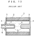
- the discharge tube 1 includes a cylindrical envelope 2 of an insulating substance such as ceramic.
- a pair of metal layers 3 are formed on the opposite end faces of the envelope 2 by suitable means such as metallization.
- a pair of electrode plates 4 are sealed in an opposing relationship to each other to the opposite end faces of the envelope 2 with the metal layers 3 interposed therebetween.
- the electrode plates 4 have electrodes 5 formed from central portions thereof which project like bars toward each other.
- Discharge gas such as argon gas is enclosed in the internal spacing of the envelope 2.
- the discharge gas is introduced into the discharge tube 1 by way of an enclosure pipe 6 securely mounted on a left-hand side one in FIG.
- the barlike electrodes 5 are positioned within the envelope 2, and the end portion of each of the electrodes 5 has a cross section of a generally semicircular shape as seen in FIG. 13.
- the electric field around the surfaces thereof and in the discharge gap G is liable to become a non-uniform electric field which varies in intensity at various locations. Consequently, the starting voltage fluctuates significantly, for example, by 20 to 30 % of the average value thereof. Also the aging is great. Accordingly, the conventional discharge tube has a problem that discharge is not stable.
- the conventional discharge tube 1 has a further problem that, when a saw-tooth voltage is applied, the starting time is fluctuated by the saw-tooth voltage and discharge is not stabilized.
- One of conventional solution to the problems is to form an electrode into a uniform electric field forming electrode which has a specific sectional shape at an end portion thereof such that the central portion thereof is formed as a flat face while a peripheral edge portion is formed as a curved face such as a Rogowski electrode, a Bruce electrode or a Harrison electrode so that the electric field around the surfaces of the electrodes and in the discharge gap is approximated to a uniform electric field in order to stabilize discharge.
- the electrode in order to form an electrode into a uniform electric field forming electrode such as a Rogowski electrode, the electrode must have a large diameter equal to three to seven times the dimension of the discharge gap. This results in the drawback that the diametrical dimension of the entire discharge tube is very large. Further, such a uniform electric field forming electrode described above requires a precision working technique for surface working and so forth. Accordingly, there is another drawback that the manufacture of the uniform electric field forming electrode is very difficult and the production costs are very high.
- each electrode is formed into a uniform electric field forming electrode, since the entire electrodes are positioned inside the envelope, if a little working error takes place in surface working, then the electric field becomes stronger at the location and discharge takes place from the portion. Accordingly, there is the possibility that discharge may be unstable.
- a discharge tube which comprises a cylindrical envelope made of an insulating substance, discharge gas enclosed in the envelope, a pair of discharge electrodes disposed in an opposing relationship to each other at the opposite ends of the envelope, the discharge electrodes being formed as parallel plate electrodes wherein faces thereof facing the inside of the envelope extend flat and in parallel to each other, and a pair of conductive layers formed on the envelope in an opposing relationship to and electrically connected to the discharge electrodes, one of the conductive layers being opposed at least part thereof with the other conductive layer with a portion of the envelope interposed therebetween.
- a discharge tube which comprises a cylindrical envelope made of an insulating substance, discharge gas enclosed in the envelope, a pair of discharge electrodes disposed in an opposing relationship to each other at the opposite ends of the envelope, and a pair of conductive layers formed corresponding to the discharge electrodes at locations on the envelope which are on the outer side with respect to an inner wall face of the envelope and at least one of which is nearer than a position at which a corresponding one of the discharge electrodes contacts with an end portion of the envelope to the companion discharge electrode, the conductive layers being electrically connected to the respective corresponding discharge electrodes.
- an electric field formed in the discharge gap between the opposing faces of the electrodes and another electric field formed in the envelope cooperate to form a uniform electric field. Consequently, the uniform electric field region formed in the discharge is very wide, and accordingly, discharge can be stabilized extremely.
- the uniform electric field region is very wide, even where the discharge gap and the inner diameter of the discharge tube are substantially egual to each other, a uniform electric field can be formed in the entire discharge tube. Consequently, the diametrical dimension of the entire discharge tube can be reduced.
- the discharge tube is generally denoted at 1 and includes several elements which have basically similar functions as those of the elements of the conventional discharge tube shown in FIG. 13, and in FIG. 1, like elements having like functions are denoted by like reference characters to those of FIG. 13 and overlapping description thereof may be omitted herein. This similarly applies to the embodiments described hereinbelow.
- the discharge tube 1 shown in FIG. 1 includes a cylindrical envelope 2 made of an insulating substance such as ceramic.
- the envelope 2 has a stepped portion 8 formed in the inside thereof such that the inner diameter r1 at one end portion 2a thereof is larger than the inner diameter r2 of the other end portion 2b thereof.
- a mounting recess 9 is thus formed at the end portion 2a of the envelope 2 by the stepped portion 8.
- An electrode 5a is fitted in the mounting recess 9.
- the electrode 5a has a generally disk-like shape and has a peripheral portion 5a' formed in a curved shape in cross section such that it is rounded toward the entrance side of the mounting recess 9.
- the inner end face 9a of the mounting recess 9 is formed as a conductive face by a metal layer 3a formed by metallization or some other suitable means, and the peripheral portion 5a' of the electrode 5a fitted in the mounting recess 9 is sealed to the inner end face 9a by soldering or some other suitable means.
- an outer end face 2b' of the other end portion 2b of the envelope 2 is formed as a conductive face by a metal layer 3b formed by metallization or some other suitable means, and a peripheral portion 5b' of another electrode 5b is sealed to the outer end face 2b' of the envelope 2.
- the electrode 5b has a generally disk-like profile and has a diameter substantially eqaual to the outer diameter of the envelope2, and the peripheral portion 5b' thereof is rounded outwardly of the envelope 2.
- An enclosure pipe 6 is securely mounted at a central portion of the electrode 5b and an enclosure hole 7 is formed at a central portion of the electrode 5b so that predetermimed discharge gas may be introduced into the discharge tube 1 by way of the enclosure pipe 6 and the enclosure hole 7.
- the peripheral portions 5a' and 5b' of the electrodes 5a and 5b of the discharge tube 1 which have curved faces are sealed to the end faces 9a and 2b' of the envelope 2, respectively, and do not face the inside of the envelope 2, but only faces 5a'' and 5b'' of the electrodes 5a and 5b, which are substantially flat and extend parallel to each other, face the inside of the envelope 2. Consequently, when a predetermined voltage is applied between the electrodes 5a and 5b, the electric field formed in a discharge spacing S between the electrode faces 5a" and 5b" is approximated to a uniform electric field.
- the sealed portion 3a for one 5a of the electrodes 5a and 5b sealed to the opposite end portions of the envelope 2 is overlapped, as viewed from the left or right in FIG. 1, with the sealed portion 3b for the other electrode 5b over an area of a portion of the envelope 2 having a dimension t1 in a radial direction. Consequently, an electric field approximated to a uniform electric field is formed also in the portion of the envelope 2.
- the electric field formed in the envelope 2 here is substantially equivalent to an electric field which is formed by the electrodes which are expanded outwardly substantially by ⁇ t1 by conversion in terms of ordinary gas in the discharge tube where ⁇ is a dielectric constant of the envelope.
- the electric field formed between the electrode faces 5a'' and 5b'' and the electric field formed in the envelope 2 cooperate with each other so that they are formed continuously. Conseguently, an electric field approximated closely to a uniform electric field is formed in the discharge spacing S by the electrode faces 5a" and 5b", and discharge is stabilized significantly since the dispersion of the starting voltage of discharge which takes place in such discharge spacing S is reduced.
- the entire bar-like electrodes are positioned in the envelope 2 and the discharging condition depends upon an electric field formed in the proximity of the discharge gap G of the electrodes 5 of the construction.
- the electric field formed in the envelope 2 is very weak, and accordingly, it has little influence upon the electric field formed in the proximity of the discharge gap G.
- a so-called uniform electric field forming electrode is employed, a uniform electric field is not formed in the entire discharge tube.
- the electric field in the envelope 2 is weak as described above, if there is a strong electric field by a neighboring conductor on the outside of the envelope 2, then in accordance with the principle of superposition, the strong electric field from the neighboring conductor has an influence on the electric field formed in the proximity of the discharge gap G. Accordingly, the conventional discharge tube has a drawback that the starting voltage is fluctuated significantly.
- the discharge tube of the present embodiment since the electrode faces 5a" and 5b" of the electrodes 5a and 5b sealed to the opposite end portions of the envelope 2 which face the inside of the envelope 2 are formed as parallel plate electrode faces and the sealed portion 3a for one 5a of the electrodes 5a and 5b which serve as one of conductive faces of the envelope 2, to which the same potentials as to those of the electrodes 5a and 5b are applied, is overlapped with the sealed portion 3b for the other electrode 5b with a portion of the envelope 2 interposed therebetween, the electric field formed between the electrode faces 5a'' and 5b'' and the electric field formed in the envelope 2 cooperate with each other. Consequently, the discharge tube produces a very wide uniform electric field region, and discharge thereof is stabilized because the dispersion of the starting voltage is reduced.
- a uniform electric field is formed only at a predetermined portion of the discharge gap but not formed in the entire discharge tube. Further, in order to form a uniform electric field at the predetermined portion, an electrode having a diameter equal to several times the dimension of the discharge gap, and consequently, the diametrical dimension of the entire discharge tube becomes very large.
- the discharge tube of the present embodiment since the unifnrm electric field region is very wide, even where the discharge gap and the inner diameter of the discharge tube are substantially equal to each other, a uniform electric field can be formed in the entire discharge tube, and as a result, the diametrical dimension of the entire discharge tube can be reduced and the discharge tube can be reduced in size comparing with the conventional discharge tube. This meanss in other words, that a large discharge gap can be obtained with a limited outer diameter of the discharge tube.
- the discharge tube is formed such that the electric field formed in the envelope 2 is close to a uniform electric field and the uniform electric field region is made very wide making use of the strong electric field, the influence of a neighboring conductor positioned on the outside of the discharge tube 1 is reduced. Consequently, the dispersion of the starting voltage arising from such neighboring conductor can be minimized.
- the curved peripheral portions 5a' and 5b' of the electrodes 5a and 5b do not face the inside of the envelope 2, the working accuracy of such curved portions does not matter at all. Consequently, the manufacture of the electrodes is facilitated very much. Further, since it is only necessary to seal such electrodes 5a and 5b to the envelope 2 having the stepped portion 8 on the inner periphery thereof to assemble them, the production costs of the discharge tube can be suppressed very low.
- the electrode 5a is fitted in the mounting recess 9 formed in the envelope 2, the distance from the electrode 5a to the other electrode 5b along the outer wall face of the envelope 2 is increased. Consequently, occurrence of creeping discharge along the outer face of the envelope 2 can be minimized or prevented and discharge can take place with a sufficiently high starting voltage between the electrode faces 5a'' and 5b''.
- the electrode 5a need not be fitted in the mounting recess 9 of the envelope 2 as described above, but it is only necessary to merely seal the electrode 5a to the end face of the envelope 2 like the other electrode 5b described above.
- sealing of the electrodes 5a and 5b may be performed at part of the conductive faces or may be performed at some other portions than the conductive faces by some other means.
- FIG. 2 there is shown a discharge tube according to a second embodiment of the present invention.
- the present discharge tube 1 is a modification or improvement to the discharge tube 1 of the first embodiment of FIG. 1.
- a pair of annular recesses 10 are formed at peripheral edge portions at the opposite axial ends of a cylindrical envelope 2, and a metal layer 3 is formed on an end face 10a of each recess 10 as a conductive face by suitable means such as metallization.
- a pair of electrodes 5a and 5b are disposed in an opposing relationship to each other at the opposite ends of the envelope 2 and are each formed substantially as a disk having a diameter substantially equal to the envelope 2. Peripheral flanged portions 11 of the electrodes 5a and 5b are sealed to the metallized end faces 10a of the recesses 10.
- the envelope 2 having the electrodes 5a and 5b sealed to the opposite end portions thereof is accommodated in and secured to the inside of a creeping discharge preventing tube 12 by way of a predetermined bonding agent 13.
- reference numeral 6 denotes an enclosure pipe for discharge gas.
- the conductive faces provided by the metallization layers 3 between the envelope 2 and the electrodes 5a and 5b and serving as the sealed portions are positioned at the outer peripheral portions of the envelope 2 and do not face the inside of the envelope 2, the electric field is weakened at locations at which the inner wall of the envelope 2 and the electrodes 5a and 5b contact with each other. Consequently, the occurrence of discharge at the locations can be prevented and further stabilized discharge can be obtained.
- the electric field formed in the envelope 2 is a little weaker than the electric field formed between the electrodes 5a'' and 5b'' due to a difference between the electric field substances so that the equipotential surface formed in the envelope 2 tends to be inclined a little from the center to the opposite end sides of the discharge tube.
- the electrodes 5a and 5b are sealed to the recessed end faces 10a of the envelope 2, the conductive faces of the envelope 2 to which potentials are applied from the electrodes 5a and 5b are disposed nearer to the companion electrode sides than the electrode faces 5a'' and 5b''. Accordingly, it is possible to correct distortion of the electric field in the envelope 2 described above so that the equipotential surfaces of the electric fields formed between the electrode faces 5a'' and 5b'' and in the the envelope 2 may be free from distortion, and the electric field formed in the discharge tube can be made further close to a uniform electric field and discharge can be further stabilized.
- the measurement proved that the average value of the starting voltage is 20 kV and the difference between the highest value and the lowest value of the starting voltage is 4.0 % or so with respect to the average value. Thus, discharge is stabilized. Further, it was proved that, even if nitrogen gas is enclosed as the discharge gas, the dispersion of the starting electrode is small.
- the electrodes 5a and 5b are sealed to the recessed end faces 10a of the envelope 2 as described above and the positions of the conductive faces and the sealed portions of the electrodes coincide with each other, if the recessed end faces 10a function as the conductive faces, then the sealed portions of the electrodes 5a and 5b to the envelope 2 may be at locations other than the recessed end faces 10a within the range in which the sealed portions by metallization do not face the inside of the envelope 2.
- the metallization faces as the conductive faces need not be parallel to each other, and for example, they may be, for example, in the form of application to the outer wall of the envelope 2.
- the creeping discharge preventing tube 12 need not be made of an insulating substance such as ceramic but may be made of plastic which is inexpensive, and if the voltage which causes external creeping discharge of the envelope 2 is higher than the starting voltage of the original discharge tube, the creeping discharge preventing tube 12 need not be employed.
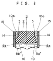
- FIG. 3 shows a modification to the discharge tube 2 shown in FIG. 2, and since, as described above, the dimension of the portion b of the envelope 2 in FIG. 2 is 0.2 mm and very small and the recessed portion 10 is formed very small and besides the curve shapes of the peripheral edge flange portions 11 of the electrodes 5a and 5b sealed to such recessed end faces 10a are very small in curvature, the electrodes 5a and 5b are each formed in a mere flat disk shape without forming the peripheral edge flange portion 11 and a soldering material 15 such as silver solder is interposed between an electrode face 14 of each of such electrodes 5a and 5b and the opposing metallized recessed end face 10a.
- a soldering material 15 such as silver solder
- the dimension of the portion b of the envelope 2 can be absorbed by a soldering margin of the soldering material 15, and the production costs of such electrodes can be further suppressed by using flat plates in the form of mere disks as the electrodes 5a and 5b.
- FIG. 4 there is shown a discharge tube according to a further embodiment of the present invention.
- the discharge tube of the present embodiment is a modification to the discharge tube 1 shown in FIG. 2 in that a pair of sputtering preventing plates 16 made of a high melting point metal such as tungsten, molybdenum or tantalum are interposed between the electrodes 5a and 5b seated to the opposite end portions of the envelope 2 and the opposite axial end faces of the envelope 2 such that the surfaces (electrode faces 5a'' and 5b'') of the electrodes 5a and 5b, facing the inside of the envelope 2, are covered with the sputtering preventing plates 16.
- the creeping discharge preventing tube 12 is not shown in FIG. 4.
- the sputtering preventing plates 16 are securely mounted at central portions of the electrodes 5a and 5b, which are formed from a material such as a 42 alloy, by welding or like means in order to make the coefficient of thermal expansion of the sputtering preventing plates 16 equal to that of the envelope 2 which is made of ceramic or a like material.
- a small gap 17 is provided around a peripheral edge of each of the sputtering preventing plates 16 in order to allow expansion and contraction of the sputtering preventing plate 16.
- the discharge tube of the present embodiment sputtering of that one of the electrodes 5a and 5b which serves as an anode can be prevented by the sputtering preventing plate 16, and consequently, soiling to the inner face of the envelope 2 arising from sputtering of the anode and occurrence of internal creeping discharge of the discharge tube arising from such soil can be prevented.
- the durability of the discharge tube can be enhanced and discharge can further be stabilized.
- the sputtering preventing plates 16 need not necessarily be provided for both of the electrodes 5a and 5b, and sufficient effects can be obtained otherwise if a sputtering preventing plate is provided for that one of the electrodes which serves as an anode.
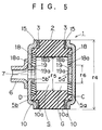
- FIGS. 5 and 6 there is shown a discharge tube according to a still further embodiment of the present invention.
- the discharge tube of the present embodiment is a modification to the discharge tube 1 of the embodiment shown in FIG. 2 in that a projecting element 18 in the form of a washer formed from an insulating substance such as ceramic similar to that of the envelope 2 and having an opening 18a at the center thereof is securely mounted at an inner peripheral portion at each of the opposite axial ends of the envelope 2 by means of a glass frit seal or the like.
- a conductive face 3 in the form of a metal layer formed by suitable means such as metallization is formed at the recessed end face 10a of an outer peripheral portion of each of the opposite ends of the envelope 2 so that the electrodes 5a and 5b may be sealed to the locations.
- the surfaces (electrode faces 5a'' and 5b'') of the electrodes 5a and 5b face the inside of the envelope 2 by way of the openings 18a of the projecting elements 18, and at such locations, a pair of sputter preventing plates 19 are disposed and securely mounted in such a manner as to cover over the electrode faces 5'' and 5b''. It is to be noted that the creeping discharge preventing tube 12 is not shown also in FIGS. 5 and 6.
- inner end faces 19a of the sputtering preventing plates 19 are positioned outwardly of the inner end faces 18b of the projecting elements 18 such that the sputtering preventing plates 19 are surrounded by the projecting elements 18.
- the recessed end faces 10a as the conduct faces are positioned inwardly of the inner end faces 18b of the projecting elements 18.
- the sputtering plate 19 which functions as an electrode is surrounded by the projecting element 18 and accordingly is surrounded by an electric field formed by the projecting element 18, the electric field formed by such projecting element 18 becomes a uniform electric field, and accordingly, the dispersion of the starting voltage can be reduced. Then, it has been cleared up that there is no problem even if the shape of the surface of the sputtering preventing plate 19 is not a flat shape.
- the working accuracy of the sputtering preventing plate 19 is sufficient even if it is not very high, and it has been cleared up that, if the peripheral edge portion of the sputtering preventing plate 19 is chamfered, then the dispersion of starting voltage can be further reduced and the discharge maintaining voltage can be reduced.
- the discharge route does not extend over the inner bore of the discharge tube and is limited to the positions around the sputtering preventing plates 19 positioned at the openings 18a of the projecting elements 18, discharge can be further stabilized, and since the sputtering preventing plates 18 have a small diameter, the costs of the sputtering preventing plates 19 can be suppressed.
- the internal creeping distance of the discharge tube 1 is elongated by the projecting elements 18, and accordingly, occurrence of inner creeping discharge can be suppressed to further stabilize discharge.
- the discharge tube of the present embodiment a measurement was conducted with the discharge tube wherein the envelope 2 is made of alumina ceramic having a dielectric constant of about 9, the outer diameter r4 of the envelope 2 is 10 mm, the inner diameter r5 is 6 mm, the dimension of the portion a in FIG. 6 is 1 mm, the dimension of the portion b is 0.2 mm, the dimension of the portion e is 0.1 mm and the dimension of the portion f is 0.5 mm, the discharge gap G between the sputtering preventing plates 19 which function as electrodes is 6 mm, the diameter r6 of the openings 18a of the projecting elements 18 is 2 mm, and the pressure of argon gas enclosed is 6 kg/cm2.
- the measurement proved that the average value of the starting voltage is 20 kV and the difference between the highest value and the lowest value of the starting voltage is 3.4 % or so with respect to the average value. Accordingly, discharge is stabilized remarkably.
- the conductive faces 3 are provided nearer to the companion electrodes than the inner end faces 18b of the projecting elements 18, this indicates an optimum condition, and it has been cleared up that, only if the conductive faces 3 are provided nearer to the companion electrodes than locations at which the electrodes 5 contact with the projecting elements 18 or the envelope 2, then the effect of making the electric field in the discharge spacing S close to a uniform electric field can be exhibited sufficiently.
- sealing of the electrodes 5 may be performed at some other portions than the recessed end faces 10a such as, for example, at end portions as indicated by C or D shown in FIG. 5 for which metallization is performed.
- FIGS. 7 to 9. there is shown a discharge tube according to a yet further embodiment of the present invention.
- discharge gas is introduced into the discharge tube 1 without using an enclosure pipe.
- a pair of projecting elements 20 formed from an insulating substance such as ceramic similar to that of an envelope 2 and each having an opening 20a at the center thereof are securely mounted in advance at inner peripheral portions at the opposite axial ends of the substantially cylindrical envelope 2 each by means of a glass frit seal or the like so that a pair of recessed portions 21 are formed at the opposite end portions of the envelope 2 having the projecting elements 20.
- a pair of substantially dish-like electrodes 5a and 5b are provided separately from the envelope 2 having the projecting elements 20.
- the electrodes 5a and 5b have formed thereon peripheral flange portions 22 which have a substantially equal diameter to that of the envelope 2 and are positioned at the recessed portions 21 when the discharge tube 1 is assembled as hereinafter described.
- a pair of sputtering preventing plates 23 are securely mounted in advance at central portions of faces of the electrodes 5a and 5b which make inner faces of the discharge tube when the discharge tube is assembled such that they may be positioned in the openings 20a of the projecting elements 20 while connecting portions 24 for communicating with the outside are securely mounted at central portions of faces which make outer faces of the discharge tube.
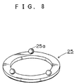
- end faces 21a of the recessed portions 21 serve as conductive faces in the form of metal layers formed by suitable means such as metallization, and such a ring-shaped solder material 25 having three protruded portions 25a formed in an eguidistantly spaced relationship on one face thereof as shown in FIG. 8 is disposed in each of the recessed portions 21 such that a face thereof on which the protruded portions 25a are not formed is opposed to the corresponding metallized end face 21a.
- the electrodes 5a and 5b having the sputtering preventing plates 23 and the connecting portions 24 are disposed at the opposite end portions of the envelope 2 which has the projecting elements 20 formed in advance thereon, with the solder materials 25 interposed between them, and a weight is placed at an upper end portion of the envelope in a condition in which the arrangement shown in FIG. 7 is rotated by 90° by means of a jig not shown.
- the entire assembly 26 is accommodated into a vessel of a gas exhausting and filling apparatus not shown, and degasification and exhaustion of air are performed while heating the assembly 26 to a sufficiently high temperature at which the solder materials 25 are not melted.
- small gaps are formed between the envelope 2 and the electrodes 5a and 5b by the protruded portions 25a of the solder materials 25 in the assembly 26, and the exhaustion of air is performed by way of the gaps.
- discharge gas such as argon gas is filled under a predetermined pressure into the vessel of the gas exhausting and filling apparatus. Further, the vessel is heated to heat the entire assembly 26 to melt the solder material 25. Thereafter, the entire assembly 26 is gradually cooled so that such a discharge tube 1 as shown in FIG. 9 which contains discharge gas such as argon gas - enclosed therein is formed.
- discharge is stabilized and the manufacture and assembly of the discharge tube is facilitated by approximating the electric field between the electrodes 5a and 5b to a uniform electric field similarly to the embodiments described above.
- sputtering can be prevented by the sputtering preventing plates 23 so that soiling to the inner face of the envelope 2 arising from sputtering at the anode and occurrence of internal creeping discharge of the discharge tube 1 arising from the soil is prevented or minimized, and besides, the internal creeping distance of the discharge tube 1 is elongated by the projecting elements 20 on the inner peripheral portions of the envelope 2 and occurrence of internal creeping discharge can be suppressed or reduced.
- the sputtering preventing plates 23 are formed so that they can be disposed in the openings 20a of the projecting elements 20, the sputtering preventing plates 23 can be formed with a small diameter, and the costs of the sputtering preventing plates 23 can be suppressed. In addition, since no enclosure pipe is reguired, the costs can be suppressed as much.
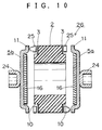
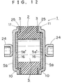
- FIGS. 10 to 12 there is shown a discharge tube according to a yet further embodiment of the present invention.
- the discharge tube of the present embodiment is a modification to the discharge tube 1 shown in FIG. 4 in that it is assembled in a procedure similar to that of the discharge tube shown in FIGS. 7 to 9 and discharge gas is enclosed in the discharge tube without using an enclosure pipe.
- the procedure is the same as that described above, it is omitted herein to avoid redundancy.
- FIGS. 1 to 6 a connecting portion for establishing communication between the discharge tube 1 and the outside is not shown, such connecting portions as shown in FIGS. 7 to 12 may be provided suitably, or the enclosure pipe 6 may be used also as a connecting portion for establishing communication with the outside.
Landscapes
- Gas-Filled Discharge Tubes (AREA)
- Cold Cathode And The Manufacture (AREA)
- Vessels And Coating Films For Discharge Lamps (AREA)
Applications Claiming Priority (2)
| Application Number | Priority Date | Filing Date | Title |
|---|---|---|---|
| JP335257/91 | 1991-12-18 | ||
| JP33525791A JP2752017B2 (ja) | 1991-12-18 | 1991-12-18 | 放電管 |
Publications (3)
| Publication Number | Publication Date |
|---|---|
| EP0547586A2 true EP0547586A2 (de) | 1993-06-23 |
| EP0547586A3 EP0547586A3 (en) | 1993-08-11 |
| EP0547586B1 EP0547586B1 (de) | 1996-02-28 |
Family
ID=18286503
Family Applications (1)
| Application Number | Title | Priority Date | Filing Date |
|---|---|---|---|
| EP92121414A Expired - Lifetime EP0547586B1 (de) | 1991-12-18 | 1992-12-16 | Entladungsrohr |
Country Status (6)
| Country | Link |
|---|---|
| US (1) | US5491381A (de) |
| EP (1) | EP0547586B1 (de) |
| JP (1) | JP2752017B2 (de) |
| KR (1) | KR970007778B1 (de) |
| CA (1) | CA2085571A1 (de) |
| DE (1) | DE69208614T2 (de) |
Cited By (2)
| Publication number | Priority date | Publication date | Assignee | Title |
|---|---|---|---|---|
| WO2003065527A1 (de) * | 2002-01-30 | 2003-08-07 | Forschungszentrum Karlsruhe Gmbh | Schaltfunkenstrecke |
| EP2648292B2 (de) † | 2007-05-22 | 2023-07-26 | Bourns, Inc. | Gasentladdungsröhre |
Families Citing this family (4)
| Publication number | Priority date | Publication date | Assignee | Title |
|---|---|---|---|---|
| JP4421191B2 (ja) * | 2003-01-30 | 2010-02-24 | 新光電気工業株式会社 | 放電管 |
| DE102005036265A1 (de) * | 2005-08-02 | 2007-02-08 | Epcos Ag | Funkenstrecke |
| TWI395252B (zh) * | 2007-05-22 | 2013-05-01 | Bourns Inc | 氣體放電管 |
| EP2959495B1 (de) * | 2013-02-22 | 2020-04-22 | Bourns Incorporated | Vorrichtungen und verfahren für flache gasentladungsröhren |
Family Cites Families (11)
| Publication number | Priority date | Publication date | Assignee | Title |
|---|---|---|---|---|
| US3253177A (en) * | 1963-03-18 | 1966-05-24 | Douglas L P Hamilton | Surge protector |
| DE1951015C3 (de) * | 1969-10-09 | 1979-02-15 | Siemens Ag, 1000 Berlin Und 8000 Muenchen | Verfahren zum Herstellen eines Überspannungsknopf ableiten |
| CH537106A (de) * | 1971-01-13 | 1973-05-15 | Siemens Ag | Uberspannungsableiter mit innerem Kurzschluss bei Überlastung |
| US4104693A (en) * | 1976-03-23 | 1978-08-01 | Reliable Electric Company | Gas filled surge arrester |
| JPS6170392U (de) * | 1984-10-15 | 1986-05-14 | ||
| GB2205992B (en) * | 1987-05-01 | 1991-07-17 | Dubilier Plc | Gas-filled surge arrestor |
| JPS6484585A (en) * | 1987-09-26 | 1989-03-29 | Matsushita Electric Works Ltd | Surge absorption element |
| FR2636167B1 (fr) * | 1988-09-08 | 1990-11-16 | Citel Cie Indle Tubes Lampes E | Parafoudre a gaz contenant un additif mineral |
| DE3833167A1 (de) * | 1988-09-27 | 1990-03-29 | Siemens Ag | Gasentladungs-ueberspannungsableiter |
| JPH0362485A (ja) * | 1989-07-28 | 1991-03-18 | Shinko Electric Ind Co Ltd | 高電圧スイッチ素子用ガス入り放電管 |
| DE4033927A1 (de) * | 1990-10-25 | 1992-04-30 | Hoechst Ceram Tec Ag | Ueberspannungsableiter |
-
1991
- 1991-12-18 JP JP33525791A patent/JP2752017B2/ja not_active Expired - Fee Related
-
1992
- 1992-12-16 CA CA002085571A patent/CA2085571A1/en not_active Abandoned
- 1992-12-16 EP EP92121414A patent/EP0547586B1/de not_active Expired - Lifetime
- 1992-12-16 DE DE69208614T patent/DE69208614T2/de not_active Expired - Fee Related
- 1992-12-17 KR KR1019920024617A patent/KR970007778B1/ko not_active Expired - Fee Related
-
1995
- 1995-01-18 US US08/375,513 patent/US5491381A/en not_active Expired - Fee Related
Cited By (2)
| Publication number | Priority date | Publication date | Assignee | Title |
|---|---|---|---|---|
| WO2003065527A1 (de) * | 2002-01-30 | 2003-08-07 | Forschungszentrum Karlsruhe Gmbh | Schaltfunkenstrecke |
| EP2648292B2 (de) † | 2007-05-22 | 2023-07-26 | Bourns, Inc. | Gasentladdungsröhre |
Also Published As
| Publication number | Publication date |
|---|---|
| CA2085571A1 (en) | 1993-06-19 |
| JPH05174704A (ja) | 1993-07-13 |
| EP0547586A3 (en) | 1993-08-11 |
| KR970007778B1 (ko) | 1997-05-16 |
| DE69208614T2 (de) | 1996-10-31 |
| DE69208614D1 (de) | 1996-04-04 |
| US5491381A (en) | 1996-02-13 |
| EP0547586B1 (de) | 1996-02-28 |
| JP2752017B2 (ja) | 1998-05-18 |
| KR930015235A (ko) | 1993-07-24 |
Similar Documents
| Publication | Publication Date | Title |
|---|---|---|
| EP0685856B1 (de) | Isolationsanordnung für ein geschweisstes hermetisches Endstück | |
| US3878423A (en) | Electrical surge arrestor having fail-safe properties | |
| KR20020044151A (ko) | 용량성 압력 센서 | |
| JPS6257933B2 (de) | ||
| EP0547586B1 (de) | Entladungsrohr | |
| KR100858071B1 (ko) | 용량식 압력 센서 | |
| JPS6213778B2 (de) | ||
| US6740838B2 (en) | Contact for vacuum interrupter and vacuum interrupter using the contact | |
| GB2314933A (en) | Capacitive differential pressure detector | |
| US4665287A (en) | Shield assembly of a vacuum interrupter | |
| US3368023A (en) | Hermetically sealed envelope structure for vacuum component | |
| US2954490A (en) | Crystal unit mounting | |
| US5391961A (en) | Gas-filled discharge tube | |
| JPH0364817A (ja) | 高電圧真空絶縁容器 | |
| US4446346A (en) | Vacuum interrupter | |
| US4733456A (en) | Method of assembling a shield assembly of a vacuum interrupter | |
| GB2278720A (en) | Electron beam tubes | |
| EP0095327B1 (de) | Vakuumschalter | |
| US5517081A (en) | Gas-filled discharge tube | |
| JP3134905B2 (ja) | サージアブソーバ | |
| US3138733A (en) | Support and spacer assembly for electron discharge tubes | |
| US3292030A (en) | Electrode assemblies for surge diverters | |
| KR860003171Y1 (ko) | 수상관용 전자총 | |
| JP2541036Y2 (ja) | マイクロ波管用高周波窓 | |
| JPH0112356Y2 (de) |
Legal Events
| Date | Code | Title | Description |
|---|---|---|---|
| PUAI | Public reference made under article 153(3) epc to a published international application that has entered the european phase |
Free format text: ORIGINAL CODE: 0009012 |
|
| AK | Designated contracting states |
Kind code of ref document: A2 Designated state(s): DE FR GB |
|
| PUAL | Search report despatched |
Free format text: ORIGINAL CODE: 0009013 |
|
| AK | Designated contracting states |
Kind code of ref document: A3 Designated state(s): DE FR GB |
|
| 17P | Request for examination filed |
Effective date: 19940210 |
|
| 17Q | First examination report despatched |
Effective date: 19941110 |
|
| GRAA | (expected) grant |
Free format text: ORIGINAL CODE: 0009210 |
|
| AK | Designated contracting states |
Kind code of ref document: B1 Designated state(s): DE FR GB |
|
| REF | Corresponds to: |
Ref document number: 69208614 Country of ref document: DE Date of ref document: 19960404 |
|
| ET | Fr: translation filed | ||
| PLBE | No opposition filed within time limit |
Free format text: ORIGINAL CODE: 0009261 |
|
| STAA | Information on the status of an ep patent application or granted ep patent |
Free format text: STATUS: NO OPPOSITION FILED WITHIN TIME LIMIT |
|
| 26N | No opposition filed | ||
| REG | Reference to a national code |
Ref country code: GB Ref legal event code: IF02 |
|
| PGFP | Annual fee paid to national office [announced via postgrant information from national office to epo] |
Ref country code: FR Payment date: 20061208 Year of fee payment: 15 |
|
| PGFP | Annual fee paid to national office [announced via postgrant information from national office to epo] |
Ref country code: GB Payment date: 20061213 Year of fee payment: 15 |
|
| PGFP | Annual fee paid to national office [announced via postgrant information from national office to epo] |
Ref country code: DE Payment date: 20061214 Year of fee payment: 15 |
|
| GBPC | Gb: european patent ceased through non-payment of renewal fee |
Effective date: 20071216 |
|
| PG25 | Lapsed in a contracting state [announced via postgrant information from national office to epo] |
Ref country code: DE Free format text: LAPSE BECAUSE OF NON-PAYMENT OF DUE FEES Effective date: 20080701 |
|
| REG | Reference to a national code |
Ref country code: FR Ref legal event code: ST Effective date: 20081020 |
|
| PG25 | Lapsed in a contracting state [announced via postgrant information from national office to epo] |
Ref country code: GB Free format text: LAPSE BECAUSE OF NON-PAYMENT OF DUE FEES Effective date: 20071216 |
|
| PG25 | Lapsed in a contracting state [announced via postgrant information from national office to epo] |
Ref country code: FR Free format text: LAPSE BECAUSE OF NON-PAYMENT OF DUE FEES Effective date: 20071231 |