EP0547989A2 - Technik zum Reduzierung von Störungen durch Alphateilchen - Google Patents
Technik zum Reduzierung von Störungen durch Alphateilchen Download PDFInfo
- Publication number
- EP0547989A2 EP0547989A2 EP92480171A EP92480171A EP0547989A2 EP 0547989 A2 EP0547989 A2 EP 0547989A2 EP 92480171 A EP92480171 A EP 92480171A EP 92480171 A EP92480171 A EP 92480171A EP 0547989 A2 EP0547989 A2 EP 0547989A2
- Authority
- EP
- European Patent Office
- Prior art keywords
- alpha
- alpha particle
- semiconductor device
- set forth
- barrier
- Prior art date
- Legal status (The legal status is an assumption and is not a legal conclusion. Google has not performed a legal analysis and makes no representation as to the accuracy of the status listed.)
- Granted
Links
Images

Classifications
-
- H—ELECTRICITY
- H10—SEMICONDUCTOR DEVICES; ELECTRIC SOLID-STATE DEVICES NOT OTHERWISE PROVIDED FOR
- H10W—GENERIC PACKAGES, INTERCONNECTIONS, CONNECTORS OR OTHER CONSTRUCTIONAL DETAILS OF DEVICES COVERED BY CLASS H10
- H10W42/00—Arrangements for protection of devices
- H10W42/20—Arrangements for protection of devices protecting against electromagnetic or particle radiation, e.g. light, X-rays, gamma-rays or electrons
- H10W42/25—Arrangements for protection of devices protecting against electromagnetic or particle radiation, e.g. light, X-rays, gamma-rays or electrons against alpha rays, e.g. for outer space applications
-
- H—ELECTRICITY
- H10—SEMICONDUCTOR DEVICES; ELECTRIC SOLID-STATE DEVICES NOT OTHERWISE PROVIDED FOR
- H10W—GENERIC PACKAGES, INTERCONNECTIONS, CONNECTORS OR OTHER CONSTRUCTIONAL DETAILS OF DEVICES COVERED BY CLASS H10
- H10W72/00—Interconnections or connectors in packages
- H10W72/20—Bump connectors, e.g. solder bumps or copper pillars; Dummy bumps; Thermal bumps
-
- H—ELECTRICITY
- H10—SEMICONDUCTOR DEVICES; ELECTRIC SOLID-STATE DEVICES NOT OTHERWISE PROVIDED FOR
- H10W—GENERIC PACKAGES, INTERCONNECTIONS, CONNECTORS OR OTHER CONSTRUCTIONAL DETAILS OF DEVICES COVERED BY CLASS H10
- H10W70/00—Package substrates; Interposers; Redistribution layers [RDL]
- H10W70/60—Insulating or insulated package substrates; Interposers; Redistribution layers
-
- H—ELECTRICITY
- H10—SEMICONDUCTOR DEVICES; ELECTRIC SOLID-STATE DEVICES NOT OTHERWISE PROVIDED FOR
- H10W—GENERIC PACKAGES, INTERCONNECTIONS, CONNECTORS OR OTHER CONSTRUCTIONAL DETAILS OF DEVICES COVERED BY CLASS H10
- H10W72/00—Interconnections or connectors in packages
- H10W72/20—Bump connectors, e.g. solder bumps or copper pillars; Dummy bumps; Thermal bumps
- H10W72/241—Dispositions, e.g. layouts
- H10W72/242—Dispositions, e.g. layouts relative to the surface, e.g. recessed, protruding
-
- H—ELECTRICITY
- H10—SEMICONDUCTOR DEVICES; ELECTRIC SOLID-STATE DEVICES NOT OTHERWISE PROVIDED FOR
- H10W—GENERIC PACKAGES, INTERCONNECTIONS, CONNECTORS OR OTHER CONSTRUCTIONAL DETAILS OF DEVICES COVERED BY CLASS H10
- H10W72/00—Interconnections or connectors in packages
- H10W72/20—Bump connectors, e.g. solder bumps or copper pillars; Dummy bumps; Thermal bumps
- H10W72/251—Materials
-
- H—ELECTRICITY
- H10—SEMICONDUCTOR DEVICES; ELECTRIC SOLID-STATE DEVICES NOT OTHERWISE PROVIDED FOR
- H10W—GENERIC PACKAGES, INTERCONNECTIONS, CONNECTORS OR OTHER CONSTRUCTIONAL DETAILS OF DEVICES COVERED BY CLASS H10
- H10W72/00—Interconnections or connectors in packages
- H10W72/20—Bump connectors, e.g. solder bumps or copper pillars; Dummy bumps; Thermal bumps
- H10W72/251—Materials
- H10W72/252—Materials comprising solid metals or solid metalloids, e.g. PbSn, Ag or Cu
-
- H—ELECTRICITY
- H10—SEMICONDUCTOR DEVICES; ELECTRIC SOLID-STATE DEVICES NOT OTHERWISE PROVIDED FOR
- H10W—GENERIC PACKAGES, INTERCONNECTIONS, CONNECTORS OR OTHER CONSTRUCTIONAL DETAILS OF DEVICES COVERED BY CLASS H10
- H10W72/00—Interconnections or connectors in packages
- H10W72/20—Bump connectors, e.g. solder bumps or copper pillars; Dummy bumps; Thermal bumps
- H10W72/29—Bond pads specially adapted therefor
-
- H—ELECTRICITY
- H10—SEMICONDUCTOR DEVICES; ELECTRIC SOLID-STATE DEVICES NOT OTHERWISE PROVIDED FOR
- H10W—GENERIC PACKAGES, INTERCONNECTIONS, CONNECTORS OR OTHER CONSTRUCTIONAL DETAILS OF DEVICES COVERED BY CLASS H10
- H10W72/00—Interconnections or connectors in packages
- H10W72/90—Bond pads, in general
- H10W72/921—Structures or relative sizes of bond pads
- H10W72/923—Bond pads having multiple stacked layers
Definitions
- the invention relates generally to methods and apparatus for reducing and/or minimizing soft errors caused by alpha particle radiation generated from within semiconductor modules of the type comprising a semiconductor device (e.g., integrated circuit) sealed in a package made, for example, of a ceramic; where a lead/tin pad (such as a C4 flip-chip contact) is located within the sealed semiconductor module and is in electrical contact with the semiconductor device. More particularly, the invention relates to methods and apparatus which minimize the potential for soft errors caused by alpha particle radiation generated by the contact, by impurities in the chip package itself and/or by certain other constituents of the semiconductor module, such as package sealing members made of low melting point glass.
- a semiconductor device e.g., integrated circuit
- a lead/tin pad such as a C4 flip-chip contact
- the aforementioned methods and apparatus are particularly useful in connection with high density- /high performance integrated circuits which cannot be easily modified (withoutaffecting circuit performance or cost), to mitigate the affects of alpha particle radiation on, for example, switching transistors, latches, etc., included in such circuits.
- the invention also relates to processes for manufacturing semiconductor modules incorporating the novel methods and apparatus set forth herein.
- pairs consisting of a positive hole and an electron are generated and either the positive hole or the electron of each pair is collected by into the active region of the semiconductor device and can cause, for example, the destruction of stored information where the semiconductor device is a memory, latch, etc. Accordingly, it is important to reduce and whenever possible minimize irradiation and intrusion of alpha rays into the active region of a semiconductor device, particularly from sources close to said active area, such as contact pads, etc.
- Abiru et al An example of a prior art teaching pertaining to the protection of semiconductor devices from alpha radiation is set forth in Abiru et al, US-A-4426657.
- Abiru et al teaches the use of a protective polyimide film layer to prevent alpha rays from intruding into a semiconductor device.
- the polyimide film layer is formed on at least one region where the semiconductor element is formed, by coating the semiconductor substrate with a liquid polyimide or polyamic acid composition having incorporated therein finely divided filler particles, according to a screen printing method.
- Abiru et al teaches a technique for preventing harmful alpha rays from intruding into a semiconductor device; this prior art reference fails to prevent such particles that emanate from within the chip itself, for example, the bottom of contact pads (such as a C4 flip-chip solder ball) on a chip. Such contact pads are known to be large generators of alpha particles that can disturb circuits on a chip.
- Otsuka et al Another example of a prior art teaching of an alpha particle shield is set forth in Otsuka et al, in USA-4541003.
- the alpha particle shield taught in the Otsuka et al reference is interposed between an alpha particle emitting resin and the active area of a semiconductor device.
- Otsuka et al like Abiru et al, fails to teach, claim or even suggest how to shield the active area of a semiconductor device from alpha radiation emanating from within the chip itself, for example, from a contact pad alpha particle source (such as a lead/tin C4 contact).
- Still another object of the invention is to provide an alpha particle shield that combines (1) the properties of an electrically insulative alpha barrier with (2) the properties of an electrically conductive alpha particle absorbing material, in order to separate a contact from the metal layers of a semiconductor device (via the shield), to thereby increase the distance between the contact (a significant alpha particle source) and the active area of the semiconductor device, and at the same time provide an electrical path between the contact and the aforesaid metal layers of the semiconductor device.
- methods, apparatus and manufacturing techniques are set forth which take advantage of the attenuation effects of well known alpha particle barriers, such as quartz or polyimide insulators; and electrically conducive studs, such as studs made of copper, which also absorb alpha particles.
- alpha particle barriers such as quartz or polyimide insulators
- electrically conducive studs such as studs made of copper, which also absorb alpha particles.
- These methods, apparatus and related manufacturing techniques are all designed to increase the vertical distance between an alpha particle source, such as a lead/tin C4 pad, and the silicon surface where the active area of an integrated circuit is located.
- the distance can be made large enough, with an alpha particle absorbing material being interposed between an alpha source and a semiconductor device, then very significant alpha particle immunity can be achieved for the semiconductor device.
- apparatus for reducing semiconductor device susceptibility to alpha particle induced soft errors in a semiconductor module that includes at least one alpha particle source and at least one semiconductor device, wherein said at least one alpha particle source includes at least one contact pad in electrical contact with the metal layers of said semiconductor device; comprising:
- apparatus for reducing alpha particle induced soft errors in a semiconductor module that includes at least one alpha particle source and at least one semiconductor device, wherein said at least one alpha particle source includes at least one contact pad in electrical contact with the metal layers of said semiconductor device, comprising means for separating said at least one contact pad from the metal layers of said semiconductor device to thereby increase the distance between said at least one contact pad and any active area of said semiconductor device.
- the invention contemplates limiting alpha radiation emitted by C4 type contacts; but also contemplates limiting the effects of alpha radiation from other alpha particle sources such as ceramic packaging, other types of contacts, package bonding material, etc.
- the invention contemplates the use of a quartz or polyimide alpha particle barrier (as an example of the aforesaid insulation means), and the use of a cylindrical copper stud inserted through the barrier provided by said insulation means, to provide an electrically conductive path between the C4 pad located on one side of the barrier and the metal layers of the semiconductor device located on the other side of the barrier.
- an alpha particle barrier comprised of the combination of (a) an alpha particle absorbing material that provides electrical insulation; and (b) an alpha particle absorbing material that provides an electrically conductive path through said material that provides electrical insulation, wherein the aforesaid combination separates at least one alpha particle source, including a contact pad, from the metal layers of a semiconductor device within a semiconductor module.
- the invention also contemplates the use of alpha particle disturbance reduction techniques which involve the step of separating a contact pad from the metal layers of a semiconductor device, where the pad and metal layers are located on opposite sides of an electrically insulative alpha absorber, and where the contact pad and metal layers are connected via an alpha particle absorbing electrically conductive path through the electrically insulative alpha absorber.
- any method that increases the distance between the active areas of a semiconductor device, and an alpha source, while interposing an alpha absorber within the region between the source and device, while at the same time providing for necessary electrical interconnections within a semiconductor module, is contemplated by the invention.
- the invention is particularly useful in solving the alpha particle disturb problem that results from alpha sources, such as contact pads, located within the semiconductor module itself.
- a semiconductor module manufacturing process which provides protection for the active area of semiconductor devices included within said module, comprising the steps of: (a) drilling at least one hole in an electrically insulative material that absorbs alpha particles, wherein said insulative material is used as an alpha particle barrier within said module to separate at least one alpha particle source, including at least one contact pad, from an active area of a semiconductor device located within said module; and (b) filling each of said at least one hole with an electrically conductive stud that has the property of absorbing alpha particles and providing an electrical path between a contact pad in contact with one end of said stud and the metal layers of said semiconductor device located on the other end of said stud on the opposite side of said barrier.
- the invention features the provision of an alpha particle disturbance reduction technique which significantly reduces the sensitivity of integrated circuits to the largest alpha particle generators, namely, the lead used in contact pads (such as C4 balls), and ceramic packages.
- the invention also provides protection against alpha rays generated by chip sealants and any other alpha emitter in close proximity to the active area of a semiconductor device that is separated from such area by the alpha barrier taught herein. Protection is provided against alpha particles traveling on either angular and vertical tracks from above the barrier toward critical device areas.
- FIG. 1 depicts a cross section of a prior art semiconductor module that includes a lead/tin C4 contact pad in direct contact with the metal layers of a semiconductor device contained within said module.
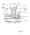
- FIG. 2 depicts a cross section of a semiconductor module fabricated in accordance with the teachings of the invention.
- FIG. 1 depicts a cross section of a prior art semiconductor module that includes a lead/tin C4 contact pad in direct contact with the metal layers of a semiconductor device contained within said module.
- FIG. 1 shows a semiconductor module 100, comprising a p-type substrate, 101, on which, for example, an n-type silicon layer 102 (such as an n-type epitaxy) is shown deposited.
- n-type silicon layer 102 such as an n-type epitaxy
- Processes for depositing n-type layer 102 on a substrate, such as substrate 101, are well known to those skilled in the art and include, for example, chemical vapor deposition techniques.
- FIG. 1 also shows, forthe sake of illustration only, transistor 103 deposed onto silicon layer 102.
- transistor 103 deposed onto silicon layer 102.
- Well known techniques also exists for fabricating, etching, depositing, etc., semiconductor devices, such as the one exemplified by transistor 103, and complete integrated circuits into layer 102 and accordingly such techniques will not be discussed further herein.
- the cross section of the semiconductor module shown in FIG. 1 also includes a depiction of the metal layers of the semiconductor device, layer(s) 104, and an exemplary electrical insulator, shown as quartz insulator 105, covering silicon epilayer 102.
- a well known type of alpha particle barrier is also shown in FIG. 1 as barrier 106.
- alpha particle barrier 106 is depicted as a 3 micron layer of electrically insulative material, such as quartz or a polyimide, covering metal layer(s) 104 and insulator 105.
- the approximately 3 micron layer of alpha absorption material shown in FIG. 1, is a common order of magnitude thickness for an absorber such as layer 106.
- a window thru alpha barrier 106 is shown, which enables the depicted lead/tin C4 contact pad, pad 107, to be affixed to metal layer(s) 104 as is conventionally done to facilitate electrical communication between the "outside world" and the semiconductor device.
- FIG. 1 also shows a portion of a ceramic cover, 110, in contact with contact 107, together with alpha particle tracks 108 and 109, indicating vertical and angular alpha tracks respectively that said alpha particles can take to adversely affect the performance of a semiconductor device, such as transistor 103.
- advantage is taken of the alpha particle attenuation effects of polyimide insulators and electrically conducting copper studs, to alleviate the alpha particle disturb problem set forth hereinabove.
- the problem can be mitigated by increasing the vertical distance between the exemplary lead/tin C4 pad shown in FIG. 1 (as pad 107) and the silicon surface (102) where exemplary transistor 103 is located. If this distance is made large enough, then very significant alpha particle immunity will be realized (by several orders of magnitude), without adding circuit components to the semiconductor device, without degrading circuit performance or increasing device cost, etc... but this is at the cost of inventing a new contact metallurgy scheme.
- FIG. 2 depicts a cross section of a semiconductor module, module 200, fabricated in accordance with the teachings of the invention.
- FIG. 2 shows an illustrative embodiment of the invention in which increased separation between a contact (such as the depicted C4 contact 207), and silicon surface 201 (including an active area, with the active area being represented in FIG. 2 by transistor 203), is accomplished by thickening the top layer insulator (205) of the chip.
- This "thickening" and “increased separation” shown in FIG. 2 is of course relative with respect to the size of barrier 106 shown in FIG. 1 (the 3 f..lm barrier). More objectively, the separation contemplated by the invention is one that distances the C4 contact itself from the metal layers of the semiconductor device.
- pad 107 in FIG. 1 is shown to be in direct contact with metal layer(s) 104; in FIG. 2, contact 207 is shown separated from metal layer(s) 204 via an electrically conducting stud, such as copper stud 206. This separation "increases" the distance between the contact and the metal layers and thus increases the vertical distance between the contact and the active area of the chip.
- FIG. 2 also shows p-type material 201, n-type material 202 (like materials 101 and 102 shown respectively in FIG. 1); alpha tracks 208 and 209; and ceramic cap 210, in contact with pad 207.
- the dashed lines at the ends of the alpha tracks shown within insulator 205 and within stud 206, are meant to show the absorption of alpha particles following the depicted tracks, with the absorption taking place before the particles have a chance to disturb transistor 203.
- the top insulator for example, a quartz or polyimide barrier between the contact pad and top layer metal
- the top insulator exhibits significant alpha particle absorption characteristics to prevent the damaging alpha particles that emanate from the contact itself (and follow a vertical track, like track 208), from adversely affecting the semiconductor device.
- Separation of pad 207 from the semiconductor device via the use of stud 206 is also effective in increasing the distance between ceramic cover 210 and the device, further protecting the device from alpha rays emanating from portions of the ceramic package (and from any sealants used) located on the opposite side of the barrier with respect to the semiconductor device.
- the standard "final vias" (holes) through the electrically insulative alpha particle barrier e.g., the window shown in layer 106 of FIG. 1 where contact pad 107 is affixed to metal layer(s) 104
- electrically conductive studs which traverse barrier 205 as shown in FIG. 2, so as to connect the lead/tin contact pad down to the top layer metal.
- this "replacement” is accomplished by drilling holes through the thick insulation layer, like layer 205 shown in FIG. 2 (for example, by RIE), and then filling the holes (for example, by plating) with electrically conducting studs, like copper stud 206, to allow electrical communication between a pad (like pad 207) and metal layer(s) 204.
- the 50 ⁇ m example for stud cross section was set forth for the purposes of illustration only and the results obtainable utilizing such a stud (in particular the exemplary cubic copper stud) are merely meant to illustrate the improvements that can be realized in alpha particle protection by utilizing combinations of various insulators and electrically conductive materials (both of which absorb alpha particles) to separate and form a barrier between alpha particle sources (including a contact pad), and active areas of a semiconductor device.
Landscapes
- Internal Circuitry In Semiconductor Integrated Circuit Devices (AREA)
- Structures Or Materials For Encapsulating Or Coating Semiconductor Devices Or Solid State Devices (AREA)
Applications Claiming Priority (2)
| Application Number | Priority Date | Filing Date | Title |
|---|---|---|---|
| US80935791A | 1991-12-17 | 1991-12-17 | |
| US809357 | 2001-03-15 |
Publications (3)
| Publication Number | Publication Date |
|---|---|
| EP0547989A2 true EP0547989A2 (de) | 1993-06-23 |
| EP0547989A3 EP0547989A3 (en) | 1993-09-01 |
| EP0547989B1 EP0547989B1 (de) | 1999-03-31 |
Family
ID=25201136
Family Applications (1)
| Application Number | Title | Priority Date | Filing Date |
|---|---|---|---|
| EP92480171A Expired - Lifetime EP0547989B1 (de) | 1991-12-17 | 1992-11-19 | Technik zum Reduzieren von Störungen durch Alphateilchen |
Country Status (3)
| Country | Link |
|---|---|
| EP (1) | EP0547989B1 (de) |
| JP (1) | JP2755360B2 (de) |
| DE (1) | DE69228792T2 (de) |
Cited By (6)
| Publication number | Priority date | Publication date | Assignee | Title |
|---|---|---|---|---|
| DE10056869A1 (de) * | 2000-11-16 | 2002-05-29 | Advanced Micro Devices Inc | Halbleiterbauteil mit einer strahlungsabsorbierenden leitenden Schutzschicht und Verfahren zur Herstellung derselben |
| EP0881676A3 (de) * | 1997-05-30 | 2005-11-09 | Lucent Technologies Inc. | Kopfüber (Flip-Chip) Verpackung von Speicherchips |
| US7348210B2 (en) | 2005-04-27 | 2008-03-25 | International Business Machines Corporation | Post bump passivation for soft error protection |
| US20090039515A1 (en) * | 2007-08-10 | 2009-02-12 | International Business Machines Corporation | Ionizing radiation blocking in ic chip to reduce soft errors |
| EP1908105A4 (de) * | 2005-07-18 | 2012-08-22 | Ibm | Verfahren und struktur zur reduktion von soft-fehlerraten in integrierten schaltungen |
| US11152378B1 (en) | 2020-03-25 | 2021-10-19 | International Business Machines Corporation | Reducing error rates with alpha particle protection |
Families Citing this family (1)
| Publication number | Priority date | Publication date | Assignee | Title |
|---|---|---|---|---|
| US8261229B2 (en) * | 2010-01-29 | 2012-09-04 | Xilinx, Inc. | Method and apparatus for interconnect layout in an integrated circuit |
Family Cites Families (3)
| Publication number | Priority date | Publication date | Assignee | Title |
|---|---|---|---|---|
| JPS5588356A (en) * | 1978-12-27 | 1980-07-04 | Hitachi Ltd | Semiconductor device |
| JPH01286448A (ja) * | 1988-05-13 | 1989-11-17 | Hitachi Ltd | 半導体装置の製造方法 |
| DE68914080T2 (de) * | 1988-10-03 | 1994-10-20 | Ibm | Kontaktständerstruktur für Halbleitervorrichtungen. |
-
1992
- 1992-11-06 JP JP4322809A patent/JP2755360B2/ja not_active Expired - Lifetime
- 1992-11-19 DE DE69228792T patent/DE69228792T2/de not_active Expired - Fee Related
- 1992-11-19 EP EP92480171A patent/EP0547989B1/de not_active Expired - Lifetime
Cited By (9)
| Publication number | Priority date | Publication date | Assignee | Title |
|---|---|---|---|---|
| EP0881676A3 (de) * | 1997-05-30 | 2005-11-09 | Lucent Technologies Inc. | Kopfüber (Flip-Chip) Verpackung von Speicherchips |
| DE10056869A1 (de) * | 2000-11-16 | 2002-05-29 | Advanced Micro Devices Inc | Halbleiterbauteil mit einer strahlungsabsorbierenden leitenden Schutzschicht und Verfahren zur Herstellung derselben |
| DE10056869B4 (de) * | 2000-11-16 | 2005-10-13 | Advanced Micro Devices, Inc., Sunnyvale | Halbleiterbauteil mit einer strahlungsabsorbierenden leitenden Schutzschicht und Verfahren zur Herstellung derselben |
| US7348210B2 (en) | 2005-04-27 | 2008-03-25 | International Business Machines Corporation | Post bump passivation for soft error protection |
| EP1908105A4 (de) * | 2005-07-18 | 2012-08-22 | Ibm | Verfahren und struktur zur reduktion von soft-fehlerraten in integrierten schaltungen |
| US20090039515A1 (en) * | 2007-08-10 | 2009-02-12 | International Business Machines Corporation | Ionizing radiation blocking in ic chip to reduce soft errors |
| US8999764B2 (en) * | 2007-08-10 | 2015-04-07 | International Business Machines Corporation | Ionizing radiation blocking in IC chip to reduce soft errors |
| US10784200B2 (en) | 2007-08-10 | 2020-09-22 | International Business Machines Corporation | Ionizing radiation blocking in IC chip to reduce soft errors |
| US11152378B1 (en) | 2020-03-25 | 2021-10-19 | International Business Machines Corporation | Reducing error rates with alpha particle protection |
Also Published As
| Publication number | Publication date |
|---|---|
| DE69228792D1 (de) | 1999-05-06 |
| DE69228792T2 (de) | 1999-10-07 |
| JPH05235000A (ja) | 1993-09-10 |
| EP0547989A3 (en) | 1993-09-01 |
| JP2755360B2 (ja) | 1998-05-20 |
| EP0547989B1 (de) | 1999-03-31 |
Similar Documents
| Publication | Publication Date | Title |
|---|---|---|
| US5998867A (en) | Radiation enhanced chip encapsulant | |
| KR101897520B1 (ko) | 신뢰성을 가지는 반도체 패키지 및 이의 제조방법 | |
| US5578874A (en) | Hermetically self-sealing flip chip | |
| EP0202109B1 (de) | Halbleiteranordnung mit hohem Widerstand gegen elektrostatische und elektromagnetische Induktion | |
| DE68920195T2 (de) | Schaltungschipspackung zum Schützen gegen elektromagnetische Interferenzen, elektrostatische Entladungen und thermische und mechanische Spannungen. | |
| US20130119523A1 (en) | Packaging structure and method and electronic device | |
| GB2039145A (en) | Semiconductor device shielding | |
| KR100608390B1 (ko) | 로우 알파 방사성 솔더 범프들 | |
| EP0547989B1 (de) | Technik zum Reduzieren von Störungen durch Alphateilchen | |
| EP0021643B1 (de) | Halbleitervorrichtung mit einer "Soft-Error"-Präventivstruktur | |
| KR100326221B1 (ko) | 반도체 장치 | |
| KR101852989B1 (ko) | 반도체 패키지 장치 | |
| JPS614250A (ja) | 半導体装置用パツケ−ジ | |
| JPS60106150A (ja) | 耐放射線パツケ−ジ | |
| US6121672A (en) | Raised pedestal radiation shield for sensitive electronics | |
| JP2870162B2 (ja) | 半導体装置およびその製造方法 | |
| CN215345692U (zh) | 空间电子设备辐照防护装置 | |
| CN113543615B (zh) | 空间电子设备辐照防护方法 | |
| KR960001614B1 (ko) | 고전압 집적회로 | |
| US6452263B1 (en) | Radiation shield and radiation shielded integrated circuit device | |
| JPS63307757A (ja) | 耐放射線型半導体装置 | |
| KR930001417B1 (ko) | 반도체 소자의 노이즈 방지방법 | |
| EP0689248B1 (de) | Integrierte Anordnung mit einer Abgrenzungsstruktur für das elektrische Oberflächenfeld und Herstellungsverfahren | |
| JPS5818961A (ja) | 集積半導体メモリのα線感応性低減装置 | |
| US20250087595A1 (en) | Mechanical mitigation of neutron see |
Legal Events
| Date | Code | Title | Description |
|---|---|---|---|
| PUAI | Public reference made under article 153(3) epc to a published international application that has entered the european phase |
Free format text: ORIGINAL CODE: 0009012 |
|
| AK | Designated contracting states |
Kind code of ref document: A2 Designated state(s): DE FR GB |
|
| PUAL | Search report despatched |
Free format text: ORIGINAL CODE: 0009013 |
|
| AK | Designated contracting states |
Kind code of ref document: A3 Designated state(s): DE FR GB |
|
| 17P | Request for examination filed |
Effective date: 19931021 |
|
| 17Q | First examination report despatched |
Effective date: 19950126 |
|
| GRAG | Despatch of communication of intention to grant |
Free format text: ORIGINAL CODE: EPIDOS AGRA |
|
| GRAG | Despatch of communication of intention to grant |
Free format text: ORIGINAL CODE: EPIDOS AGRA |
|
| GRAH | Despatch of communication of intention to grant a patent |
Free format text: ORIGINAL CODE: EPIDOS IGRA |
|
| GRAH | Despatch of communication of intention to grant a patent |
Free format text: ORIGINAL CODE: EPIDOS IGRA |
|
| GRAA | (expected) grant |
Free format text: ORIGINAL CODE: 0009210 |
|
| AK | Designated contracting states |
Kind code of ref document: B1 Designated state(s): DE FR GB |
|
| REF | Corresponds to: |
Ref document number: 69228792 Country of ref document: DE Date of ref document: 19990506 |
|
| ET | Fr: translation filed | ||
| PLBE | No opposition filed within time limit |
Free format text: ORIGINAL CODE: 0009261 |
|
| 26N | No opposition filed | ||
| PGFP | Annual fee paid to national office [announced via postgrant information from national office to epo] |
Ref country code: GB Payment date: 20001101 Year of fee payment: 9 |
|
| PGFP | Annual fee paid to national office [announced via postgrant information from national office to epo] |
Ref country code: FR Payment date: 20001120 Year of fee payment: 9 |
|
| PG25 | Lapsed in a contracting state [announced via postgrant information from national office to epo] |
Ref country code: GB Free format text: LAPSE BECAUSE OF NON-PAYMENT OF DUE FEES Effective date: 20011119 |
|
| PGFP | Annual fee paid to national office [announced via postgrant information from national office to epo] |
Ref country code: DE Payment date: 20011122 Year of fee payment: 10 |
|
| REG | Reference to a national code |
Ref country code: GB Ref legal event code: IF02 |
|
| GBPC | Gb: european patent ceased through non-payment of renewal fee |
Effective date: 20011119 |
|
| PG25 | Lapsed in a contracting state [announced via postgrant information from national office to epo] |
Ref country code: FR Free format text: LAPSE BECAUSE OF NON-PAYMENT OF DUE FEES Effective date: 20020730 |
|
| REG | Reference to a national code |
Ref country code: FR Ref legal event code: ST |
|
| REG | Reference to a national code |
Ref country code: FR Ref legal event code: ST |
|
| PG25 | Lapsed in a contracting state [announced via postgrant information from national office to epo] |
Ref country code: DE Free format text: LAPSE BECAUSE OF NON-PAYMENT OF DUE FEES Effective date: 20030603 |