EP0548882A1 - Hybrides optisch/elektrisches Schaltkreismodul - Google Patents
Hybrides optisch/elektrisches Schaltkreismodul Download PDFInfo
- Publication number
- EP0548882A1 EP0548882A1 EP92121703A EP92121703A EP0548882A1 EP 0548882 A1 EP0548882 A1 EP 0548882A1 EP 92121703 A EP92121703 A EP 92121703A EP 92121703 A EP92121703 A EP 92121703A EP 0548882 A1 EP0548882 A1 EP 0548882A1
- Authority
- EP
- European Patent Office
- Prior art keywords
- optical
- electrical
- converter
- radiation fin
- fin assembly
- Prior art date
- Legal status (The legal status is an assumption and is not a legal conclusion. Google has not performed a legal analysis and makes no representation as to the accuracy of the status listed.)
- Ceased
Links
Images








Classifications
-
- H—ELECTRICITY
- H10—SEMICONDUCTOR DEVICES; ELECTRIC SOLID-STATE DEVICES NOT OTHERWISE PROVIDED FOR
- H10W—GENERIC PACKAGES, INTERCONNECTIONS, CONNECTORS OR OTHER CONSTRUCTIONAL DETAILS OF DEVICES COVERED BY CLASS H10
- H10W90/00—Package configurations
-
- G—PHYSICS
- G02—OPTICS
- G02B—OPTICAL ELEMENTS, SYSTEMS OR APPARATUS
- G02B6/00—Light guides; Structural details of arrangements comprising light guides and other optical elements, e.g. couplings
- G02B6/24—Coupling light guides
- G02B6/42—Coupling light guides with opto-electronic elements
- G02B6/4201—Packages, e.g. shape, construction, internal or external details
- G02B6/4249—Packages, e.g. shape, construction, internal or external details comprising arrays of active devices and fibres
-
- H—ELECTRICITY
- H01—ELECTRIC ELEMENTS
- H01S—DEVICES USING THE PROCESS OF LIGHT AMPLIFICATION BY STIMULATED EMISSION OF RADIATION [LASER] TO AMPLIFY OR GENERATE LIGHT; DEVICES USING STIMULATED EMISSION OF ELECTROMAGNETIC RADIATION IN WAVE RANGES OTHER THAN OPTICAL
- H01S5/00—Semiconductor lasers
- H01S5/02—Structural details or components not essential to laser action
- H01S5/024—Arrangements for thermal management
-
- H—ELECTRICITY
- H01—ELECTRIC ELEMENTS
- H01S—DEVICES USING THE PROCESS OF LIGHT AMPLIFICATION BY STIMULATED EMISSION OF RADIATION [LASER] TO AMPLIFY OR GENERATE LIGHT; DEVICES USING STIMULATED EMISSION OF ELECTROMAGNETIC RADIATION IN WAVE RANGES OTHER THAN OPTICAL
- H01S5/00—Semiconductor lasers
- H01S5/02—Structural details or components not essential to laser action
- H01S5/022—Mountings; Housings
- H01S5/0233—Mounting configuration of laser chips
- H01S5/02345—Wire-bonding
Definitions
- the present invention relates to a hybrid optical/electrical circuit module designed so as to provide a communication between a communications apparatus and a computer.
- the hybrid optical/electrical circuit modules are generally classified into two types: an E/O (electrical/optical) module that converts an electric signal to an optical signal and delivers it to the transmission line and an O/E (optical/electrical) module that receives an optical signal from the transmission line and converts it to an electric signal.
- E/O electric/optical
- O/E optical/electrical
- Fig. 22 is a schematic block diagram of an E/O module using a laser diode (LD).
- An electric signal is a ternary signal taking one of three values: +, 0 and -, while an optical signal is a binary signal that is either on or off.
- An electric signal coming from a transmission line is converted to a binary signal in an interface circuit, changed in transmission speed, scrambled in an encoder circuit and connected to an optical/electrical converter.
- the electric signal is converted to an optical on/off signal by LD and delivered to the transmission line using an optical fiber.
- the interface circuit, encoder circuit, and LD drive circuit are made of a silicon bipolar LSI, GaAs LSI or the like, and the laser diode (LD) is made of a GaAs, InP or the like semiconductor.
- LD has a temperature dependence of about 1 mA (drive current)/°C between the drive current and optical output as shown in Fig. 23.
- the temperature dependence varies from one type of LD to another. Therefore, for assuring a stable optical output, a circuit has to be provided which changes the drive current according to the temperature. For simplifying or omitting this circuit, it is necessary to stabilize the temperature around LD by eliminating the thermal influence from other devices.
- the electric circuit and E/O converter have a boundary between the encoder circuit and LD drive circuit.
- the present invention is not limited to such an arrangement, but the boundary may be provided between the LD drive circuit and LD. Namely, the electric circuit and E/O converter may be so defined.
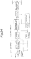
- Fig. 24 is a schematic block diagram of an O/E module using an avalanche photodiode (APD).
- a received optical signal from an optical fiber is converted to a current signal by the avalanche photodiode (APD) and amplified.
- the current signal is further amplified by an equalizing amplifier.
- the amplifier has a varied DC level depending upon the on-off ratio (ratio between on and off) of the signal.
- a DC regenerative circuit is required for keeping the DC level constant by suppressing the DC variation, and to this end, a clamping circuit is utilized.
- the output of the clamping circuit is passed through an automatic gain control (AGC) circuit intended to provide an output level with a dynamic range, a clock recovery circuit for discrimination, regeneration and other logical processing and a discriminator/regenerator circuit for discriminating between "1" and "0" and thus taken as an electric signal.
- AGC automatic gain control
- the boundary between the O/E converter and electric circuit lies between the equalizing amplifier and the clamping circuit.
- the present invention is not limited to this arrangement, but the boundary may be laid in other places.
- the avalanche photodiode is made of an InP./In GaAs semiconductor and other circuits are made of a silicon bipolar LSI, GaAs LSI or the like.
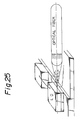
- Fig. 25 shows the geometrical relation between the LD and the optical fiber
- Fig. 26 shows the relation between the misalignment of the optical axis between the LD and the optical fiber and the coupling loss.
- SM single mold fiber
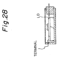
- Figs. 27 and 28 show a conventional electric circuit and E/O converter, respectively.
- the development of thermal stress and mechanical stress in the E/O converter must be minimized during assembly and after the alignment of the optical axis between the optical fiber and the optical element.
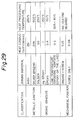
- LSI and fins should preferably be joined by a metal junction using a solder or an AuSn alloy or by a junction using a high-temperature conductive organic adhesive, from the standpoint of heat radiation.
- these junction methods are to be done at a temperature as high as 150°C or more as shown in Fig. 29.
- the power consumption of the E/O and/or O/E converter is small compared with that of the electric circuit.
- packages are formed for the E/O and/or O/E converter and the electric circuit, respectively.
- the E/O and/or O/E converter package is assembled by a low temperature process with priority given to the alignment of optical axis while the electric circuit package is assembled by a high temperature process primarily for heat radiation. These packages are mounted separately on a mother board.
- the present invention has an object to overcome the above-mentioned drawbacks and inconsistency in design and lower the manufacturing costs by reducing the number of components and improving the manufacturabiity of the optical/electrical circuit module. Namely, the present invention seeks to solve the following problems:
- a hybrid optical/electrical circuit module comprising: a radiation fin assembly; an electric circuit that includes no or substantially no optical parts, and is secured to said radiation fin assembly by a first securing means superior in heat conductivity, such that heat from said electric circuit may by effectively removed; and an optical/electrical converter and/or electrical converter to be electrically connected with said electric circuit, which includes a decoder and/or coder, and is secured to said radiation fin assembly by a second securing means with no or only a small amount of heat generated thereby, so as not to thermally influence each other.
- Figs. 1 to 3 show an embodiment of the hybrid optical/electrical circuit module according to the present invention.
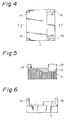
- the hybrid optical/electrical circuit module (will be referred to as "module” hereafter) 1 according to the present invention comprises an electric circuit 4 and a E/O and/or O/E converter 5 integrally mounted on a radiation fin assembly 3 having four stems 3a and 3b shown in Figs. 4 to 6.
- the electric circuit 4 has a high-temperature radiation substrate 7 joined directly to the top of the radiation fin assembly 3.
- Various components mounted on the high-temperature radiation substrate 7 are covered with a sealing case 8.
- the reference numeral 10 denotes interconnecting terminals that electrically connect the electric circuit 4 to the outside.
- the interconnecting terminals 10 are joined to the high-temperature radiation substrate 7 by a silver brazing. Namely, these interconnecting terminals 10 are not adapted to penetrate, as in the conventional module (as in Figs. 27 and 28), the Kovar-made case housing the electric circuit (see the detail view of the terminal in Fig. 27).
- the pitch of the interconnecting terminals 10 can be extremely (1 mm or less) and the module can be produced at a reduced cost.
- the E/O and/or O/E converter 5 is fixed as fitted in a recess 12 formed in the radiation fin assembly 3 at a level one step lower than the top of the latter and it is electrically connected to the electric circuit 4.
- the E/O and/or O/E converter 5 is fixed with a screw 31.
- the E/O and/or O/E converter 5 itself is hermetically sealed, which will be discussed in further detail later.
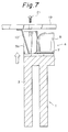
- the interconnecting terminals 10 on the radiation fin assembly 3 are put in contact with and engaged on the circuit board 19 with a predetermined clearance defined between the circuit board 19 and the stems 3a of the radiation fin assembly 3 (module 1).
- the interconnecting terminals 10 are elastically deformed so that a predetermined contact pressure develops between the circuit board 19 and interconnecting terminals 10.
- the interconnecting terminals thus in contact with the circuit board 19 are soldered to the latter, which ensures a reliable junction.
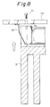
- the interconnecting terminal may be slightly bent at the middle thereof as shown in Fig. 8 (terminal 10').
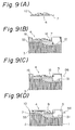
- SMD is mounted on the high-temperature radiation substrate 7 and wire-bonded to form the electric circuit 4 (as in Fig. 9(A)).
- the electric circuit 4 is joined to the radiation fin assembly 3 made of an aluminum alloy with a silicon adhesive layer 33 made of, for example, a high-temperature conductive resin in a heating/bonding process in which a low thermal resistance is ensured (as in Fig. 9(B)).
- the electric circuit 4 has mounted thereon mainly highly heat-dissipative LSIs that will not be thermally influenced by the heating process in which the maximum temperature is in the order of 200°C.
- the E/O and/or O/E converter 5 having optical fibers 14 projecting outward is fitted in the recess 12 formed in the right end portion of the radiation fin assembly 3 at a level one step lower than the latter, and fixed by a fixing means with no heat (no-heating process), for example, screw 31 (as in Fig. 9(C)).
- the electric circuit 4 and E/O and/or O/E converter 5 are electrically connected to each other, and the resistor and capacitor on the electric circuit 4 are adjusted for a predetermined circuit characteristic.
- the junction between the electric circuit and E/O or O/E converter is described in detail below.
- the E/O and/or O/E converter 5 is inserted into the electric circuit integrated with the radiation fin assembly as guided by the recess formed in the latter.
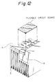
- Figs. 11 and 12 are sectional views, enlarged in scale, of the junction between the electric circuit 4 and E/O and/or O/E converter 5.
- the interconnecting terminals of the electric circuit and E/O and/or O/E converter are aligned to each other and guided by the recess in the radiation fin assembly. These terminals are electrically connected to each other by wire bonding (as in Fig. 11) or a flexible circuit board (as in Fig. 12).
- the electric circuit 4 is sealed and encased with the sealing case made of Kovar by utilizing the welding stem provided on the outer circumference of the electric circuit on the high-temperature radiation substrate (as in Fig. 9(D)).
- the hybrid optical/electrical circuit module 1 is completed safely, and easily.
- the electric circuit 4 and E/O and/or O/E converter 5 are mounted together on the radiation fin assembly 3 being a common base for both the electric circuit and the E/O and/or O/E converter, so the entire module 1 is extremely compact. Also, since the manufacturing process is simplified and facilitated, the cost and yield of production can be greatly improved. Furthermore, the electric circuit 4 is sealed separately from the E/O and/or O/E converter 5, so the module 1 can be easily repaired and the E/O and/or O/E converter 5 can be easily replaced. Moreover, since the high-temperature radiation substrate 7 and radiation fin assembly 3 are joined directly to each other, so that the thermal resistance is lower and heat can be efficiently radiated. Thus, the module 1 is more stable and reliable.
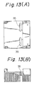
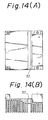
- the radiation fin assembly 3 In place of the radiation fin assembly 3 detailed in Figs. 4 to 6, there may be formed in areas where the electric circuit and E/O and/or O/E converter are mounted, respectively, elongated holes 35, for example, as shown in Fig. 13 to divide the radiation fin assembly into two blocks thermally isolated from each other, thereby protecting the E/O and/or O/E converter 5, which is easily influenced by heat. Otherwise, as shown in Fig. 14, the radiation fin assembly 3 may be divided into two blocks by the above-mentioned areas and a non-heat conductive material, for example, an epoxy resin member 37, may be inserted between such blocks, whereby the heat transferred from the radiation fin assembly on which the electric circuit is mounted can be effectively shut off.
- a non-heat conductive material for example, an epoxy resin member 37
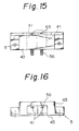
- the E/O and/or O/E converter 5 is made of two photo-coupling blocks 41 inserted into a photo-coupling holder 43 made of aluminum and fixed with a low-temperature setting adhesive 45 (for example, an epoxy resin settable at 80°C).
- a low-temperature setting adhesive 45 for example, an epoxy resin settable at 80°C.
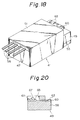
- the photo-coupling block 41 consists, as shown in Figs. 17 and 18, of a fiber block 47, and LD block 49 that is mounted on the fiber block 47, and a U-shaped cover 51 made of Kovar that is put on both blocks 47 and 49 and laser-welded at the contact faces thereof.
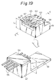
- the fiber block 47 has a base portion 53 made of Kovar and a keep plate 54 also made of Kovar, as shown in Fig. 19.
- the keep plate 54 retains four parallel optical fibers 56 under it on the top of the fiber block 47. Gold is deposited on the optical fibers at the covered portions. These three members 53, 54 and 56 are joined by soldering.
- the dimension L1 (as shown in Fig. 19) from the reference surface on the base portion 53 to the center of the optical fibers 56 is in the order of plus or minus several microns per tenths.
- the LD block 49 comprises a base portion 58 made of Kovar, an AlN substrate 60 fixed as soldered to the base portion 58, and four LDs (laser diodes) 61 fixed in parallel formation on the substrate 60.
- the substrate 60 provides, at the rear thereof, an external interconnecting terminal 63 for electrical connection with the outside, and each bonding pad 65 of the electric circuit provided at the opposite side of the substrate is connected to a corresponding LD 61 by a bonding wire 67.
- the dimension L2 from the reference surface (bottom) to the LD light emitter 69 of LD is equal to L1 and it is in the order of plus or minus several microns per tenths.
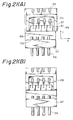
- the fiber block 47 and LD block 47 are optically coupled to each other by setting the LD block 49 on the fiber block 47 (as in Fig. 19), sliding the LD block 49 in X- and Y-directions (as in Fig. 21) and aligning it so that misalignment of the optical axis is several microns or less.
- the Y-directional dimensions of the end face of the optical fiber 56 and LD 61 are normally 20 to 50 microns. After aligning, both members 47 and 49 are joined together by laser spot-welding or the like.
- the present invention overcomes the drawbacks of the prior art and provides a hybrid optical/electrical circuit module highly reliable and stable that can be easily manufactured at less cost.
Landscapes
- Physics & Mathematics (AREA)
- General Physics & Mathematics (AREA)
- Optics & Photonics (AREA)
- Condensed Matter Physics & Semiconductors (AREA)
- Electromagnetism (AREA)
- Optical Couplings Of Light Guides (AREA)
- Electric Connection Of Electric Components To Printed Circuits (AREA)
- Cooling Or The Like Of Electrical Apparatus (AREA)
- Structure Of Printed Boards (AREA)
- Cooling Or The Like Of Semiconductors Or Solid State Devices (AREA)
- Semiconductor Lasers (AREA)
- Led Devices (AREA)
Applications Claiming Priority (2)
| Application Number | Priority Date | Filing Date | Title |
|---|---|---|---|
| JP33883991A JPH05175520A (ja) | 1991-12-20 | 1991-12-20 | 光電気回路混載モジュール |
| JP338839/91 | 1991-12-20 |
Publications (1)
| Publication Number | Publication Date |
|---|---|
| EP0548882A1 true EP0548882A1 (de) | 1993-06-30 |
Family
ID=18321912
Family Applications (1)
| Application Number | Title | Priority Date | Filing Date |
|---|---|---|---|
| EP92121703A Ceased EP0548882A1 (de) | 1991-12-20 | 1992-12-21 | Hybrides optisch/elektrisches Schaltkreismodul |
Country Status (3)
| Country | Link |
|---|---|
| US (1) | US5324936A (de) |
| EP (1) | EP0548882A1 (de) |
| JP (1) | JPH05175520A (de) |
Cited By (2)
| Publication number | Priority date | Publication date | Assignee | Title |
|---|---|---|---|---|
| EP0682277A1 (de) * | 1994-05-10 | 1995-11-15 | Radiall | Anordnung zur Verbindung von optischen Fasern und Wellenleitern, die auf einem Substrat angebracht sind |
| GB2271682B (en) * | 1992-10-13 | 1997-03-26 | Marconi Gec Ltd | Improvements in or relating to connectors |
Families Citing this family (4)
| Publication number | Priority date | Publication date | Assignee | Title |
|---|---|---|---|---|
| DE4303780C1 (de) * | 1993-02-05 | 1994-08-04 | Siemens Ag | Elektro-optischer Modul |
| JP4936581B2 (ja) * | 1999-06-29 | 2012-05-23 | 京セラ株式会社 | 光モジュールの接続構造体 |
| US6840685B1 (en) * | 1999-06-29 | 2005-01-11 | Kyocera Corporation | Optical module and connecting construction for optical module |
| JP4844196B2 (ja) * | 2006-03-30 | 2011-12-28 | 株式会社日立製作所 | 放射線検出回路 |
Citations (2)
| Publication number | Priority date | Publication date | Assignee | Title |
|---|---|---|---|---|
| US4803361A (en) * | 1986-05-26 | 1989-02-07 | Hitachi, Ltd. | Photoelectric device with optical fiber and laser emitting chip |
| US4884125A (en) * | 1986-10-15 | 1989-11-28 | Sanyo Electic Co., Ltd. | Hybrid integrated circuit device capable of being inserted into socket |
Family Cites Families (3)
| Publication number | Priority date | Publication date | Assignee | Title |
|---|---|---|---|---|
| US4234790A (en) * | 1979-02-01 | 1980-11-18 | The Perkin-Elmer Corporation | Photodetector heat stabilizer |
| US4575629A (en) * | 1983-12-29 | 1986-03-11 | Uop Inc. | Detector for raman spectra and other weak light |
| JPS62281453A (ja) * | 1986-05-30 | 1987-12-07 | Hitachi Ltd | チツプキヤリアモジユ−ル |
-
1991
- 1991-12-20 JP JP33883991A patent/JPH05175520A/ja not_active Withdrawn
-
1992
- 1992-12-18 US US07/993,110 patent/US5324936A/en not_active Expired - Lifetime
- 1992-12-21 EP EP92121703A patent/EP0548882A1/de not_active Ceased
Patent Citations (2)
| Publication number | Priority date | Publication date | Assignee | Title |
|---|---|---|---|---|
| US4803361A (en) * | 1986-05-26 | 1989-02-07 | Hitachi, Ltd. | Photoelectric device with optical fiber and laser emitting chip |
| US4884125A (en) * | 1986-10-15 | 1989-11-28 | Sanyo Electic Co., Ltd. | Hybrid integrated circuit device capable of being inserted into socket |
Non-Patent Citations (5)
| Title |
|---|
| PATENT ABSTRACTS OF JAPAN vol. 13, no. 496 (E-843)9 November 1989 & JP-A-01 199 483 ( HITACHI LTD ) * |
| PATENT ABSTRACTS OF JAPAN vol. 13, no. 5 (E-701)9 January 1989 & JP-A-63 217 648 ( HITACHI LTD ) * |
| PATENT ABSTRACTS OF JAPAN vol. 14, no. 142 (E-904)16 March 1990 & JP-A-02 007 455 ( NEC CORP ) * |
| PATENT ABSTRACTS OF JAPAN vol. 15, no. 46 (E-1029)4 February 1991 & JP-A-02 278 782 ( NEC CORP ) * |
| PATENT ABSTRACTS OF JAPAN vol. 15, no. 98 (E-1042)8 March 1991 & JP-A-02 306 656 ( TOSHIBA CORP ) * |
Cited By (4)
| Publication number | Priority date | Publication date | Assignee | Title |
|---|---|---|---|---|
| GB2271682B (en) * | 1992-10-13 | 1997-03-26 | Marconi Gec Ltd | Improvements in or relating to connectors |
| EP0682277A1 (de) * | 1994-05-10 | 1995-11-15 | Radiall | Anordnung zur Verbindung von optischen Fasern und Wellenleitern, die auf einem Substrat angebracht sind |
| FR2719912A1 (fr) * | 1994-05-10 | 1995-11-17 | Radiall Sa | Dispositif de connexion de fibres optiques à des guides d'ondes formés dans un substrat. |
| US5555331A (en) * | 1994-05-10 | 1996-09-10 | Radiall | Device for connecting optical fibres to waveguides formed in a substrate |
Also Published As
| Publication number | Publication date |
|---|---|
| JPH05175520A (ja) | 1993-07-13 |
| US5324936A (en) | 1994-06-28 |
Similar Documents
| Publication | Publication Date | Title |
|---|---|---|
| US6155724A (en) | Light transmitting module for optical communication and light transmitting unit thereof | |
| US6635866B2 (en) | Multi-functional fiber optic coupler | |
| US4997243A (en) | Method of mounting a light emitting chip and an optical fiber on a photoelectric device | |
| US4268113A (en) | Signal coupling element for substrate-mounted optical transducers | |
| US5960141A (en) | Optical transmission terminal device | |
| US5309460A (en) | Semiconductor laser with encapsulated lead members | |
| US6425695B1 (en) | Optical module and method of manufacturing the same | |
| CA1292798C (en) | Semiconductor laser module of dual in-line package type | |
| EP0529947A1 (de) | Optische Baugruppe mit einer Faserbefestigungsvorrichtung | |
| US20040120660A1 (en) | Optical device and optical module | |
| US6624507B1 (en) | Miniature semiconductor package for opto-electronic devices | |
| EP0596613A2 (de) | Faseroptische Kopplungsmodule | |
| US20010017964A1 (en) | Optical interconnection module | |
| US7136594B2 (en) | Optical communication device | |
| JPH06237016A (ja) | 光ファイバモジュールおよびその製造方法 | |
| JP2004214651A (ja) | 光モジュール | |
| US5589402A (en) | Process for manufacturing a package for mating with a bare semiconductor die | |
| US4184070A (en) | Connector apparatus | |
| GB2126795A (en) | Optical device | |
| US5324936A (en) | Hybrid optical/electrical circuit module with thermal insulation | |
| US6646291B2 (en) | Advanced optical module which enables a surface mount configuration | |
| US20040179793A1 (en) | Optoelectronic device packaging assemblies and methods of making the same | |
| US20040247259A1 (en) | A to-can having a leadframe | |
| JPH10247741A (ja) | 光通信用発光モジュールおよびその組立方法 | |
| JP3717623B2 (ja) | 光電子装置およびその製造方法 |
Legal Events
| Date | Code | Title | Description |
|---|---|---|---|
| PUAI | Public reference made under article 153(3) epc to a published international application that has entered the european phase |
Free format text: ORIGINAL CODE: 0009012 |
|
| AK | Designated contracting states |
Kind code of ref document: A1 Designated state(s): DE FR GB |
|
| 17P | Request for examination filed |
Effective date: 19930614 |
|
| 17Q | First examination report despatched |
Effective date: 19941223 |
|
| GRAG | Despatch of communication of intention to grant |
Free format text: ORIGINAL CODE: EPIDOS AGRA |
|
| STAA | Information on the status of an ep patent application or granted ep patent |
Free format text: STATUS: THE APPLICATION HAS BEEN REFUSED |
|
| 18R | Application refused |
Effective date: 19971016 |