EP0549155A2 - Steuerungssystem für optische Datenplatten - Google Patents
Steuerungssystem für optische Datenplatten Download PDFInfo
- Publication number
- EP0549155A2 EP0549155A2 EP92310965A EP92310965A EP0549155A2 EP 0549155 A2 EP0549155 A2 EP 0549155A2 EP 92310965 A EP92310965 A EP 92310965A EP 92310965 A EP92310965 A EP 92310965A EP 0549155 A2 EP0549155 A2 EP 0549155A2
- Authority
- EP
- European Patent Office
- Prior art keywords
- sector
- sector mark
- pattern
- pseudo
- signal
- Prior art date
- Legal status (The legal status is an assumption and is not a legal conclusion. Google has not performed a legal analysis and makes no representation as to the accuracy of the status listed.)
- Withdrawn
Links
Images




Classifications
-
- G—PHYSICS
- G11—INFORMATION STORAGE
- G11B—INFORMATION STORAGE BASED ON RELATIVE MOVEMENT BETWEEN RECORD CARRIER AND TRANSDUCER
- G11B20/00—Signal processing not specific to the method of recording or reproducing; Circuits therefor
- G11B20/10—Digital recording or reproducing
- G11B20/12—Formatting, e.g. arrangement of data block or words on the record carriers
- G11B20/1217—Formatting, e.g. arrangement of data block or words on the record carriers on discs
- G11B20/1252—Formatting, e.g. arrangement of data block or words on the record carriers on discs for discontinuous data, e.g. digital information signals or computer program data
-
- G—PHYSICS
- G11—INFORMATION STORAGE
- G11B—INFORMATION STORAGE BASED ON RELATIVE MOVEMENT BETWEEN RECORD CARRIER AND TRANSDUCER
- G11B11/00—Recording on or reproducing from the same record carrier wherein for these two operations the methods are covered by different main groups of groups G11B3/00 - G11B7/00 or by different subgroups of group G11B9/00; Record carriers therefor
-
- G—PHYSICS
- G11—INFORMATION STORAGE
- G11B—INFORMATION STORAGE BASED ON RELATIVE MOVEMENT BETWEEN RECORD CARRIER AND TRANSDUCER
- G11B19/00—Driving, starting, stopping record carriers not specifically of filamentary or web form, or of supports therefor; Control thereof; Control of operating function ; Driving both disc and head
- G11B19/02—Control of operating function, e.g. switching from recording to reproducing
- G11B19/04—Arrangements for preventing, inhibiting, or warning against double recording on the same blank or against other recording or reproducing malfunctions
-
- G—PHYSICS
- G11—INFORMATION STORAGE
- G11B—INFORMATION STORAGE BASED ON RELATIVE MOVEMENT BETWEEN RECORD CARRIER AND TRANSDUCER
- G11B20/00—Signal processing not specific to the method of recording or reproducing; Circuits therefor
- G11B20/10—Digital recording or reproducing
- G11B20/18—Error detection or correction; Testing, e.g. of drop-outs
- G11B20/1816—Testing
-
- G—PHYSICS
- G11—INFORMATION STORAGE
- G11B—INFORMATION STORAGE BASED ON RELATIVE MOVEMENT BETWEEN RECORD CARRIER AND TRANSDUCER
- G11B27/00—Editing; Indexing; Addressing; Timing or synchronising; Monitoring; Measuring tape travel
- G11B27/10—Indexing; Addressing; Timing or synchronising; Measuring tape travel
- G11B27/19—Indexing; Addressing; Timing or synchronising; Measuring tape travel by using information detectable on the record carrier
- G11B27/28—Indexing; Addressing; Timing or synchronising; Measuring tape travel by using information detectable on the record carrier by using information signals recorded by the same method as the main recording
- G11B27/30—Indexing; Addressing; Timing or synchronising; Measuring tape travel by using information detectable on the record carrier by using information signals recorded by the same method as the main recording on the same track as the main recording
- G11B27/3027—Indexing; Addressing; Timing or synchronising; Measuring tape travel by using information detectable on the record carrier by using information signals recorded by the same method as the main recording on the same track as the main recording used signal is digitally coded
-
- G—PHYSICS
- G11—INFORMATION STORAGE
- G11B—INFORMATION STORAGE BASED ON RELATIVE MOVEMENT BETWEEN RECORD CARRIER AND TRANSDUCER
- G11B20/00—Signal processing not specific to the method of recording or reproducing; Circuits therefor
- G11B20/10—Digital recording or reproducing
- G11B2020/10916—Seeking data on the record carrier for preparing an access to a specific address
-
- G—PHYSICS
- G11—INFORMATION STORAGE
- G11B—INFORMATION STORAGE BASED ON RELATIVE MOVEMENT BETWEEN RECORD CARRIER AND TRANSDUCER
- G11B20/00—Signal processing not specific to the method of recording or reproducing; Circuits therefor
- G11B20/10—Digital recording or reproducing
- G11B20/14—Digital recording or reproducing using self-clocking codes
- G11B20/1403—Digital recording or reproducing using self-clocking codes characterised by the use of two levels
- G11B2020/1476—Synchronisation patterns; Coping with defects thereof
-
- G—PHYSICS
- G11—INFORMATION STORAGE
- G11B—INFORMATION STORAGE BASED ON RELATIVE MOVEMENT BETWEEN RECORD CARRIER AND TRANSDUCER
- G11B2220/00—Record carriers by type
- G11B2220/20—Disc-shaped record carriers
-
- G—PHYSICS
- G11—INFORMATION STORAGE
- G11B—INFORMATION STORAGE BASED ON RELATIVE MOVEMENT BETWEEN RECORD CARRIER AND TRANSDUCER
- G11B2220/00—Record carriers by type
- G11B2220/20—Disc-shaped record carriers
- G11B2220/25—Disc-shaped record carriers characterised in that the disc is based on a specific recording technology
- G11B2220/2525—Magneto-optical [MO] discs
Definitions
- This invention relates generally to data recovery from optical data disks, and more particularly to data recovery from sectors of disks having missing or defective sector marks.
- Optical disk media are capable of storing a considerable amount of data in the form of small marks or holes in the surface of the disk, each representing a bit of data.
- the marks, burned into the surface of the disk by a laser, are arranged along spiral tracks, each divided into a number of sectors.
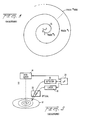
- Figure 5 is a diagram of an apparatus 10 for reading data prerecorded on an optical disk 12.
- the disk 12 is rotated by a disk servo 14 comprising a precisely controllable DC motor.
- a laser 16 irradiates the surface of the disk 12, and light reflected from the disk impinges on the surface of a detector 18.
- An optical head 20, located between the disk 12 and laser/detector 16, 18, is positioned by another servo (not shown) to read data from a desired track.
- Writing is carried out using similar optics, with the optical medium being preheated to enable light from laser 16 to form surface marks corresponding to data.
- the servos and laser/detector are controlled by a microprocessor 22.
- the components comprising apparatus 10 shown in Figure 5 typically are arranged within a common housing, such as provided by SCSI (Small Computer System Interface) resident at a personal computer or other computer requiring storage of a large quantity of data.
- SCSI Small Computer System Interface
- the data storage capacity of the disk 12 is enhanced in some systems by utilizing both sides of a disk such as a 130mm (5 1/4 inch) optical disk.
- Data read and write logic implemented by microprocessor 22 in the representative illustration of Figure 5, has been carried out by commercially available special function integrated circuits, such as the AM95C96 optical disk controller (ODC), manufactured by Advanced Micro Devices of Sunnyvale, California.
- ODC optical disk controller
- ODC optical disk controller
- PLL phase locked loop
- a CPU 32 controls seeking to the desired location on the disk.
- the ODC/ODE 24, 28 interfaces with CPU 32, working memory 34 and a disk interface 36 to process the applied data signals and transfer commands for compliance with particular specifications such as the X3B11 continuous composite servo (CCS), WORM/ERASABLE optical format developed by ANSI.
- CCS continuous composite servo
- WORM/ERASABLE optical format developed by ANSI.
- the ODC 24 is interfaced to a system bus by host interface unit 38, and is supported by buffer memory 40 and error processor 42.
- buffer memory 40 and error processor 42 General operation of the system shown in Figure 1, being known to the prior art, is not described in detail.
- An improvement integrating the ODC/ODE 24,26 as a single functional element is described in my copending application S.N. , filed concurrently herewith.
- Figure 4 depicts the layout of tracks on an optical disk.
- the tracks are arranged along a spiral path on the surface of the disk 12, with each turn of the spiral being treated as a separate track.
- the optical disk may be 90mm in diameter, and may contain 10,000 tracks (numbered 0-9999 in Figure 7); each track is divided into twenty-five (25) sectors. Each sector in turn-will carry 725 bytes of unformatted data.
- the optical disk in this example is capable of storing 181,250,000 bytes of data, or about 100,000 pages of text. Modifications include implementing more densely packed sectors, larger diameter disks and/or double- sided storage for enhanced information storage capacity.
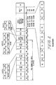
- Figure 2 is a field diagram of the X3B11 format, comprising a header area that is "pre-stamped", followed by a data area for receiving data for storage.
- the first field of the header is a sector mark (SM) having a special redundant pattern. This field identifies the start of a sector.
- SM sector mark
- ODE 26 detects sector mark (SM) once within each sector.
- SM sector mark
- the sector mark comprises 80 bits arranged as a long burn followed by a transition pattern.
- Sector mark decoding is carried out by monitoring the long burn pattern of the track, and identifying a pattern characteristic of the sector mark.
- Detection of the sector mark pattern is a prerequisite to recovery of data from the corresponding sector. It provides synchronization to the region of each sector from which data is to be recovered or is to be written.
- the data field of each sector resides at a predefined distance, in bytes, from the end of the sector mark pattern. The number of bytes depends on the particular standard involved. For example, in the conventional X3B11 format, shown symbolically in Figure 2, the pre-stamped, or read only (RO), region extends 47 bytes beyond the sector mark field SM, followed by a magneto-optic region (MO) upon which data can be written once (the MO region is also termed a "WORM", or write once-read many, region).
- the data region of a 90mm, 512 byte sector size by convention follows the RO region by ODF and GAP bytes.
- the next sector mark field follows the data field by a buffer region of 13 bytes for timing margins.
- Prior art optical data disk controllers improve data recovery from optical disks by searching the track of an optical data disk for the presence of sector mark patterns in the appropriate fields, and applying a pseudo sector mark pattern to each sector in which a sector mark pattern is not detected.
- a "sector mark found" signal is issued.
- a data recovery routine is initiated to access data from the data field of the current sector. Data recovery from a sector having a defective sector mark field thus is achieved.
- the disk has a considerable number of sectors with defective sector marks, the disk itself may be defective, and should not be used. The user should be appraised of the possibly defective quality of a disk before data is written to it.
- Optical data disks are supplied in any of several formats.
- the format of a new, unmarked disk may have to be ascertained by the user in a procedure termed "certification.”
- certification it is desirable to implement media certification without imposing a requirement for additional equipment.
- Our control system implements sector mark detection as a mechanism for media certification of an optical data disk.
- an optical data disk controller optically detects bits from a track of an optical data disk adapted to contain data arranged in sectors.
- a predefined region of the track is searched for the presence of a pattern of bits corresponding to a sector mark identifying the beginning of each sector from which data is to be recovered. If no sector mark is found, a pseudo sector mark signal is generated to recover data from the sector.
- writing to the data field of a sector for which a pseudo sector mark signal has been generated is inhibited. The pseudo sector mark found signals are counted, and no pseudo sector mark found signals are generated in excess of a predetermined number.
- the track of an optical disk is searched for the presence of a normal sector mark pattern.
- a predefined region of the next sector where the sector mark pattern is expected is searched using a window of programmable width.
- a pseudo sector mark signal is generated for each sector in which no sector mark is detected. The search repeats until either a predetermined number of pseudo sector mark signals are generated, a normal sector mark pattern is detected or an exit command is received.
- the disk in a constant sector mark mode the disk is searched, with the window wide open, to detect sector mark patterns continuously for media certification.
- Sector mark pattern detection and pseudo sector mark signal generation is preferably carried out, in accordance with the invention, by programming CPU 32 of the prior art system of Figure 1 or by the preferred implementation of Figure 6 described in my copending application.
- Programming identified by the numeral 60 in Figure 3, is characterized by two principal routines or loops, a "normal loop” 66 and a pseudo sector mark (PSM) loop 76.
- the normal loop 66 is continuously executed while normal sector mark patterns are detected in the sector mark field of successive sectors.
- the PSM loop 76 is executed to generate pseudo sector mark signals for sectors within which no sector mark pattern has been detected.
- the program 60 jumps between one loop and the other, dynamically, depending upon the outcome of a sector mark pattern search for each sector of an optical data disk.
- Another routine implemented by step 86, carries out media certification by searching for and reporting sector mark patterns continuously.
- the program 60 first carries out system initialization including a hardware reset routine and setting of initial command states (step 62). The program then enters a first sector mark loop 64, searching for the sector mark pattern with a wide open "search window".
- search window refers to a pattern search without consideration of any predefined region within which the desired pattern or a portion of the pattern is expected to be found.
- a sector mark found (SMF) signal is issued, and program 60 advances to normal loop 66, where the position of the next sector mark field is ascertained by counting down in succession (1) the number of bytes comprising the RO region (step 68), (2) the number comprising the MO region (step 70) and (3) a remainder (step 72) depending upon the format of the standard involved.
- SMF sector mark found
- the pre-formatted region (RO) extending beyond the sector mark field is 47 bytes in length.
- the RO count for step 68 preprogrammed by the user, is preset to 47 bytes.
- the magneto-optic region MO from the beginning of the ODF/GAP/FLAG field to the middle of the buffer field BUFF, is 667 bytes in length.
- the MO count for step 70 thus is preset to 667.
- the program 60 next searches for a sector mark pattern in the field by opening a search window to a width preprogrammed by the user (step 74).
- the size of the window establishes the robustness of the search, and in the preferred embodiment the window is programmable between a minimum of 1 byte and a maximum of seven bytes in width.
- the size of the sector mark window is programmed in accordance with sector format.
- the size of the window in accordance with the preferred embodiment, is preprogrammed to have the widths shown in the following Table II.
- a narrow window will identify a sector mark pattern that occurs in the expected position.
- a wider window examines a larger portion of the sector for a sector mark pattern that may be displaced in the sector due to disk rotation speed.
- an SMF signal is generated by step 74, and the program returns to step 68 where another sector mark pattern in the next sector mark field is searched.
- a sector identification sequence is initiated in response to the SMF signal to identify the desired sector. Hence, when the desired sector is identified, data in the data field of the sector is read in the usual manner.
- Step 74 if no sector mark pattern is found, the program jumps from step 74 to the PSM loop 76, where a pseudo sector mark signal is generated.
- Step 78 issues a PSM found signal and generates an SMF, if preprogrammed.
- an interrupt with status also is supplied.
- the pseudo sector mark signal initiates the desired sector identification, and hence, data field read.
- step 80 With the search window wide open (step 80), the RO region is counted down. Upon a countdown to zero, writing to the data field optionally is inhibited, a feature that prevents writing to a sector having a defective sector mark. If this option is not pre-selected, writing to the data field of a sector having a defective sector mark pattern is carried out. With the search window still wide open, the MO count is next counted down in Step 82. If a sector mark pattern is detected during step 80 or 82, an SMF signal, together with optional interrupt/status signal, is generated, indicating that the sector may possibly be defective (a sector mark pattern should reside only in the sector mark field). However, following step 82, and counting down further by the remainder count in the buffer field BUFF, the presence of the sector mark in the next sector mark field is searched with a wide open window until the remainder count is counted down (step 84).
- step 84 the program returns to step 68 of the normal loop 66 to search for another normal sector mark pattern. If no sector mark pattern is detected, the program returns to step 78 of the PSM loop, another pseudo sector mark signal is generated, and steps 78 - 84 are repeated. These steps can be repeated indefinitely or a preselected number of times, for example, four times.
- the number of pseudo sector mark signals is counted during execution of the PSM loop 76, and if more than the preselected number (e.g., 4) has been generated, the disk is deemed to be possibly defective, and the program exits the PSM loop to return to the first SM loop at step 64, where a normal sector mark is searched with the window wide open.
- a normal sector mark is searched with the window wide open.
- an interrupt signal is generated indicating that the preselected count has been exceeded.
- the data previously read may optionally be discarded as being unreliable.
- the program may optionally exit the PSM loop if a "forced exit” option is pre-programmed. In this case, the program will exit the PSM loop immediately, as shown at step 84 of Figure 3.
- step 86 the program jumps directly to step 86, where the medium is searched for sector mark patterns with the search window wide open.
- a sector mark found SMF signal is generated each time a sector mark pattern is detected using a wide open detection window.
- the frequency of sector mark pattern during detection can be monitored by observing the SMF signal to ascertain the format of a disk under test or confirm that the disk is functional.
- This mode can also be used for customized or any non-X3B11 formats.
Landscapes
- Engineering & Computer Science (AREA)
- Signal Processing (AREA)
- General Engineering & Computer Science (AREA)
- Signal Processing For Digital Recording And Reproducing (AREA)
- Optical Recording Or Reproduction (AREA)
Applications Claiming Priority (2)
| Application Number | Priority Date | Filing Date | Title |
|---|---|---|---|
| US81057691A | 1991-12-24 | 1991-12-24 | |
| US810576 | 1991-12-24 |
Publications (2)
| Publication Number | Publication Date |
|---|---|
| EP0549155A2 true EP0549155A2 (de) | 1993-06-30 |
| EP0549155A3 EP0549155A3 (en) | 1993-11-18 |
Family
ID=25204151
Family Applications (1)
| Application Number | Title | Priority Date | Filing Date |
|---|---|---|---|
| EP19920310965 Withdrawn EP0549155A3 (en) | 1991-12-24 | 1992-12-01 | Optical data disk control system |
Country Status (3)
| Country | Link |
|---|---|
| EP (1) | EP0549155A3 (de) |
| JP (1) | JPH05242485A (de) |
| KR (1) | KR930014370A (de) |
Cited By (1)
| Publication number | Priority date | Publication date | Assignee | Title |
|---|---|---|---|---|
| EP1096491A1 (de) * | 1999-10-26 | 2001-05-02 | Iomega Corporation | Synchronisationsrückgewinnungstechnik für Speichermedien |
Family Cites Families (6)
| Publication number | Priority date | Publication date | Assignee | Title |
|---|---|---|---|---|
| JPH0760574B2 (ja) * | 1984-03-26 | 1995-06-28 | 株式会社日立製作所 | 光デイスク装置のセクタ開始信号発生回路 |
| JPH0721936B2 (ja) * | 1986-05-16 | 1995-03-08 | 松下電器産業株式会社 | 情報記録再生装置 |
| US4833663A (en) * | 1987-01-16 | 1989-05-23 | Matsushita Electric Industrial Co., Ltd. | Information recording/reproducing apparatus for handling defective sectors on an optical disk |
| US5083303A (en) * | 1988-04-28 | 1992-01-21 | Olympus Optical Co., Ltd. | Sector mark detecting apparatus in optical disc apparatus |
| EP0428411B1 (de) * | 1989-11-16 | 1996-02-07 | Canon Kabushiki Kaisha | Informationsverarbeitungsgerät |
| JP2998161B2 (ja) * | 1990-01-17 | 2000-01-11 | 富士通株式会社 | 記録媒体の同期信号読取方法及び装置 |
-
1992
- 1992-12-01 EP EP19920310965 patent/EP0549155A3/en not_active Withdrawn
- 1992-12-22 JP JP4342340A patent/JPH05242485A/ja not_active Withdrawn
- 1992-12-24 KR KR1019920025472A patent/KR930014370A/ko not_active Withdrawn
Cited By (2)
| Publication number | Priority date | Publication date | Assignee | Title |
|---|---|---|---|---|
| EP1096491A1 (de) * | 1999-10-26 | 2001-05-02 | Iomega Corporation | Synchronisationsrückgewinnungstechnik für Speichermedien |
| US6557113B1 (en) | 1999-10-26 | 2003-04-29 | Iomega Corporation | Synchronization recovery technique for storage media |
Also Published As
| Publication number | Publication date |
|---|---|
| EP0549155A3 (en) | 1993-11-18 |
| KR930014370A (ko) | 1993-07-23 |
| JPH05242485A (ja) | 1993-09-21 |
Similar Documents
| Publication | Publication Date | Title |
|---|---|---|
| EP0549151A2 (de) | Steuerungssysteme für optische Datenplatten | |
| EP0584504B1 (de) | Bandformaterkennungssystem | |
| US5757568A (en) | System and method for encoding a servo address | |
| EP0265849B1 (de) | Verfahren und Gerät zur optischen Aufnahme/Wiedergabe | |
| EP0144813A1 (de) | Gerät zur Aufzeichnung und Wiedergabe | |
| JPH04232665A (ja) | データ記憶装置 | |
| JP2662491B2 (ja) | サーボマークパターン生成及び検出方法 | |
| DE19911469A1 (de) | Verfahren zur Wiedergewinnung der Daten von einer Platte mit einem dynamischen Irrungs-Offset-Daten-Wiedergewinnungsprotokolls mit einem Fehlerkorrekturcode | |
| US5268802A (en) | Reading non-standard tapes on tape drives | |
| US5444685A (en) | Sector mark pattern detection for optical data disk controller | |
| EP0549152A2 (de) | Einchipsteuerung für optische Datenlaufwerke | |
| US6104558A (en) | System and method of encoding an index mark into a servo address | |
| EP0549155A2 (de) | Steuerungssystem für optische Datenplatten | |
| US4819092A (en) | Apparatus for writing signal density information on a magnetic medium | |
| JP3155663B2 (ja) | 光ディスク装置 | |
| EP0390510B1 (de) | Optisches Gerät zur Datenwiedergabe | |
| EP0478323A2 (de) | Verfahren zur Bestimmung des Inhaltes und der Richtigkeit von Prüfdatenanordnungen in Datenspeichersysteme mit beweglichen Medien | |
| US5237552A (en) | Sector mark detection in long burn pattern for optical data disks | |
| JP2571669B2 (ja) | 光学ドライブコントローラ及び光学ディスクドライブ並びに情報読み取り方法 | |
| EP0549153B1 (de) | Erfassung der Sektormarkierungen für optische Datenplatten | |
| DE19547815A1 (de) | Lese-/Schreib-Vorrichtung und Adressenerkennungs-Verfahren bei derselben | |
| EP0549154A2 (de) | Erkennung eines wiederholenden Musters | |
| JPS62275304A (ja) | 磁気記録再生装置 | |
| JPH05266593A (ja) | 光ディスク装置 | |
| JP2644862B2 (ja) | 光ディスク装置 |
Legal Events
| Date | Code | Title | Description |
|---|---|---|---|
| PUAI | Public reference made under article 153(3) epc to a published international application that has entered the european phase |
Free format text: ORIGINAL CODE: 0009012 |
|
| AK | Designated contracting states |
Kind code of ref document: A2 Designated state(s): AT BE CH DE DK ES FR GB GR IE IT LI LU NL PT SE |
|
| PUAL | Search report despatched |
Free format text: ORIGINAL CODE: 0009013 |
|
| AK | Designated contracting states |
Kind code of ref document: A3 Designated state(s): AT BE CH DE DK ES FR GB GR IE IT LI LU NL PT SE |
|
| 17P | Request for examination filed |
Effective date: 19940513 |
|
| 17Q | First examination report despatched |
Effective date: 19951228 |
|
| GRAG | Despatch of communication of intention to grant |
Free format text: ORIGINAL CODE: EPIDOS AGRA |
|
| GRAG | Despatch of communication of intention to grant |
Free format text: ORIGINAL CODE: EPIDOS AGRA |
|
| GRAH | Despatch of communication of intention to grant a patent |
Free format text: ORIGINAL CODE: EPIDOS IGRA |
|
| 18D | Application deemed to be withdrawn |
Effective date: 19980319 |