EP0549320A1 - Verfahren und Vorrichtung für ESD-Schutz - Google Patents
Verfahren und Vorrichtung für ESD-Schutz Download PDFInfo
- Publication number
- EP0549320A1 EP0549320A1 EP92311688A EP92311688A EP0549320A1 EP 0549320 A1 EP0549320 A1 EP 0549320A1 EP 92311688 A EP92311688 A EP 92311688A EP 92311688 A EP92311688 A EP 92311688A EP 0549320 A1 EP0549320 A1 EP 0549320A1
- Authority
- EP
- European Patent Office
- Prior art keywords
- gate
- esd
- nmos
- voltage
- drain
- Prior art date
- Legal status (The legal status is an assumption and is not a legal conclusion. Google has not performed a legal analysis and makes no representation as to the accuracy of the status listed.)
- Granted
Links
Images



Classifications
-
- H—ELECTRICITY
- H10—SEMICONDUCTOR DEVICES; ELECTRIC SOLID-STATE DEVICES NOT OTHERWISE PROVIDED FOR
- H10D—INORGANIC ELECTRIC SEMICONDUCTOR DEVICES
- H10D89/00—Aspects of integrated devices not covered by groups H10D84/00 - H10D88/00
- H10D89/60—Integrated devices comprising arrangements for electrical or thermal protection, e.g. protection circuits against electrostatic discharge [ESD]
- H10D89/601—Integrated devices comprising arrangements for electrical or thermal protection, e.g. protection circuits against electrostatic discharge [ESD] for devices having insulated gate electrodes, e.g. for IGFETs or IGBTs
- H10D89/811—Integrated devices comprising arrangements for electrical or thermal protection, e.g. protection circuits against electrostatic discharge [ESD] for devices having insulated gate electrodes, e.g. for IGFETs or IGBTs using FETs as protective elements
- H10D89/813—Integrated devices comprising arrangements for electrical or thermal protection, e.g. protection circuits against electrostatic discharge [ESD] for devices having insulated gate electrodes, e.g. for IGFETs or IGBTs using FETs as protective elements specially adapted to provide an electrical current path other than the field-effect induced current path
- H10D89/814—Integrated devices comprising arrangements for electrical or thermal protection, e.g. protection circuits against electrostatic discharge [ESD] for devices having insulated gate electrodes, e.g. for IGFETs or IGBTs using FETs as protective elements specially adapted to provide an electrical current path other than the field-effect induced current path involving a parasitic bipolar transistor triggered by the electrical biasing of the gate electrode of the FET, e.g. gate coupled transistors
-
- H—ELECTRICITY
- H01—ELECTRIC ELEMENTS
- H01F—MAGNETS; INDUCTANCES; TRANSFORMERS; SELECTION OF MATERIALS FOR THEIR MAGNETIC PROPERTIES
- H01F1/00—Magnets or magnetic bodies characterised by the magnetic materials therefor; Selection of materials for their magnetic properties
- H01F1/01—Magnets or magnetic bodies characterised by the magnetic materials therefor; Selection of materials for their magnetic properties of inorganic materials
- H01F1/03—Magnets or magnetic bodies characterised by the magnetic materials therefor; Selection of materials for their magnetic properties of inorganic materials characterised by their coercivity
- H01F1/0302—Magnets or magnetic bodies characterised by the magnetic materials therefor; Selection of materials for their magnetic properties of inorganic materials characterised by their coercivity characterised by unspecified or heterogeneous hardness or specially adapted for magnetic hardness transitions
- H01F1/0306—Metals or alloys, e.g. LAVES phase alloys of the MgCu2-type
Definitions
- This invention relates to integrated circuits, and more particularly, relates to electrostatic discharge protection devices for incorporation into integrated circuits.
- Electronic integrated circuits often fail when exposed to large and sudden electrostatic discharges.
- the manufacture and use of integrated circuits in equipment and by personnel may result in the build up of substantial amounts of charge dig the contact and subsequent removal of dissimilar materials from one another.
- the built up electrostatic charge may be quickly discharged when the charged items comes in contact with an integrated circuit, especially when portions of the circuit are connected to power supplies that have an equipment ground.
- Such discharges may cause significant damage to the integrated circuit by way of dielectric breakdown of oxides and other thin films and by high levels of conduction through relatively small areas of the circuit arising from reverse breakdown of P-N junctions of the circuit.
- the diode If the diode enters the negative resistance region of its diode breakdown characteristics, sufficient conduction may occur to melt conductive material (such as polysilicon or aluminum), via resistive heating, causing especially damaging results. The molten material may then flow along the lines of the electric field associated with the device and create a short circuit, such as a source-to-drain short in a MOSFET. This short circuit will remain after the electrostatic discharge has been completed and is likely to render the integrated circuit useless.
- conductive material such as polysilicon or aluminum
- output buffer circuits have not included ESD devices for various reasons.
- the transistors in the push-pull output buffer have been sufficiently large to safely handle the fairly large amounts of electrostatic discharge current that may be presented at the output terminal.
- the performance of the output terminal relative to electrostatic discharge protection was thus often better than the input terminals of the device. Improvements in ESD protection for the input terminals of integrated circuits beyond the protection provided by the push-pull output drive circuit has shifted the emphasis of electrostatic discharge protection back to the output buffer. Process advancements have also contributed to the degradation of an output circuit's ESD levels.
- the output buffer may be provided with an improved ESD tolerance by incorporating a field oxide (or other high threshold voltage) transistor, having its source-to-drain path connected between the ground and the gate of the pull-down transistor, and having its gate connected to the output terminal.
- a field oxide (or other high threshold voltage) transistor having its source-to-drain path connected between the ground and the gate of the pull-down transistor, and having its gate connected to the output terminal.
- An example of such an output buffer having improved ESD tolerance is described in U.S. Patent No. 4,855,620, issued August 8, 1989 and assigned to Texas Instruments Incorporated.
- This patent describes a thin oxide NMOS output device coupled with a field oxide device to ground the gate of the thin oxide device during ESD and help improve the ESD protection level.
- the grounding of the gate was an attempt to suppress the MOSFET channel conductions while the parasitic bipolar (npn) device discharged the electrostatic stress current.
- npn parasitic bipolar
- method and apparatus are provided for ESD protection of integrated circuits.
- the methods of the present invention employ dynamic gate coupling effects between an NMOS device and a field oxide device to achieve uniform conduction of the MOSFET device fingers and provide a much improved ESD protection for integrated circuits.
- the apparatus of the present invention employs a field oxide device and an NMOS device whose gate is connected to the drain of the field oxide device.
- the sources of the NMOS and the field oxide devices are connected to ground, while both the drain of the NMOS device and gate of the field oxide device are connected to an output, input, or other signal terminal to be protected from ESD events.
- an N-well resistor is connected between the gate of the NMOS device and ground.
- the operation of the apparatus of the present invention is involved with simultaneous MOS/bipolar conduction.
- the voltage at the drain of the NMOS and at the gate of the field oxide device both increase.
- the MOSFET gate potential also increases, by an amount depending upon the field oxide device size.
- the turn-on threshold voltage of the field oxide device is reached, the field oxide device will turn on, ground its drain via the grounded source, and thereby discharge the MOSFET gate to ground.
- the NMOS device with its gate at 1-2 volts and its drain at 10 to 12 volts will be under high substrate current conditions due to impact ionization at the drain.
- the resultant hole injection into the substrate will forward bias the MOSFET source junction and thereby uniformly turn on the lateral fingers of the parasitic npn device for efficient ESD protection.
- the N-well resistor serves to discharge any non-ESD charge buildup on the gate of the NMOS device to ground.
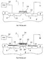
- Figure 1 is a cross-sectional diagram of an N-channel pull-down transistor of an output buffer constructed by conventional methods.
- Figure 2 is a cross-sectional diagram of an N-channel pull-down transistor having clad diffusions constructed by conventional methods, illustrating channel inversion resulting from capacitive coupling of an ESD pulse to the gate.
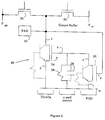
- Figure 3 is an electrical diagram, in schematic form, of the ESD apparatus of the present invention connected to an output buffer.
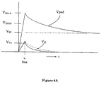
- Figure 4A depicts a drain waveform and a gate waveform for an NMOS device during an ESD event.
- Figure 4B depicts current versus voltage waveforms for an NMOS device during an ESD event.
- Figure 5A is an electrical diagram, in schematic form, of the ESD apparatus of the present invention connected to the input buffer of a device.
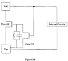
- Figure 5B is an electrical diagram, in schematic form, of the ESD apparatus of the present invention used for internal protection between two voltages.
- Figure 6 is a cross-sectional diagram of an NMOS device and a metal gate field oxide device which may be used as the apparatus of the present invention.
- Transistor 2 is constructed in p-type substrate 4.
- This substrate 4 may, of course, alternatively be formed by epitaxial layer growth upon a substrate 4, or even by a p-type well diffused into an n-type substrate or epitaxial layer, such as in a CMOS device.
- the drain 6 and source 8 of transistor 2 are formed by n-type diffusions into the substrate 4.
- its source 8 is connected to ground, and its drain 6 is connected to the output terminal or pad 10.
- Field oxide layers 9 isolate the n-type diffusions of transistor 2 from neighboring transistors, in a manner well known in the art.
- the channel region lying between the source and drain is covered by a gate dielectric 12, over which a gate terminal 14 is deposited and patterned.
- the gate dielectric 12 is generally silicon dioxide, while the gate terminal 14 is generally polycrystalline silicon.
- the drain 6 and source 8 regions are diffused after the gate dielectric 12 and the gate electrode 14 are in place, for self-alignment with the gate electrode 14.
- the metallization forming contacts to the gate electrode 14, drain region 6 and source region 8 are not shown in Figure 1 for the sake of simplicity.
- transistor 2 In the event of a substantial voltage pulse (of a negative potential relative to ground) on the pad 10, such as may occur in an ESD event, transistor 2 is able to quickly handle the resultant current. Since the substrate 4 is generally biased to ground, or to a negative voltage, a negative voltage or drain 6 will forward bias the p-n junction 15 between the drain 6 and substrate 4. Accordingly, the charge applied to the pad 10 by the negative ESD event is safely conducted into substrate 4 without damage to transistor 2.
- the resultant breakdown current would be conducted from the pad 10 to the source region 8 connected to ground.
- damage to transistor 2 may result from localized heating due to this breakdown current conduction.
- Such localized heating is determined by the product of the local current density and the electric field (J-E product).
- the J-E product is likely to be locally highest at the p-n junction 15 in a breakdown condition.
- the likelihood of damage to transistor 2 due to this condition will depend to a large degree upon the spacing separating the metallization (i.e., the source of metal filaments) from the point of localized heating at the p-n junction 15, i.e. the spacing between the metal contact to the drain 6 and the gate electrode 14.
- transistor 2 using the lightly-doped-drain, or graded junction, construction and using silicide-clad diffusions is illustrated.
- sidewall oxide spacers 16 may be formed along the edges of gate dielectric 12 and gate electrode 14, resulting in a shallower junction depth of the drain regions 6 and source regions 8 near the transistor channel region, as shown in Figure 2.
- silicide 18 such as titanium silicide.
- Titanium silicide formation is accomplished by way of a direct react process after deposition of a titanium layer, as is well known in the art and as described in U.S. Patent Nos. 4,384,301 and 4,545,116, both assigned to Texas Instruments Incorporated.
- the use of these advanced process techniques may result in reduced failure thresholds for ESD events. It is believed that the factors of (a) greater localized heating due to the increase in the J-E product at the surface of the channel region results from the shallower junction depth of the graded junction and (b) greater availability of melt material from the silicide layer 18 closer to the localized heating, contribute to the reduced ESD failure thresholds for these technologies.
- the ESD apparatus 33 of the present invention is a separate circuit connected between the output and V SS or ground of the output buffer 30, 32.
- This separate ESD protection circuit 33 only operates upon an ESD pulse and does not interfere with the normal operation of the output buffer.
- the ESD protection circuit of the present invention may also be employed as the output buffer.
- the ESD apparatus 33 of the present invention consists of an NMOS device 34 whose gate 34g is connected to the drain 36d of a field oxide device 36.
- the sources of the NMOS 34s and the field oxide 36s devices are connected to V SS or ground, while the drain of the NMOS 34d and the gate of the field oxide 36d devices are connected to the output or pad 10.
- an N-well resistor 38 is connected to the gate 34g of the NMOS device and to V SS or ground.
- This N-well resistor 38 has an inherent capacitance 39 associated with it.
- the RC constant of the resistor's resistance and capacitance should be long with respect to the rise time for ESD events while being short with respect to normal operating and measurement conditions.
- the voltages at drain 34d of the NMOS and the gate 36g of the field oxide device both increase.
- the dotted line components in Figure 3 illustrate how the solid line components operate during an ESD event.
- the N-well resistor 38 is solid since it may also operate during non-ESD events. Due to capacitive coupling between the drain 34d and gate 34g of the NMOS device, the MOSFET gate 36g potential also increases, which can be about 1 to 2 volts, depending upon the size of the field oxide device 36 and the N-well resistor 38. As the size of the field oxide device 36 increases the capacitance between the substrate and the drain 36d of the field oxide device increases.
- the NMOS device 34 Prior to this, however, the NMOS device 34, with its gate 34g at 1-2 volts and its drain 34d at 10 to 12 volts, will be under high substrate current conditions due to impact ionization at the drain.
- the resultant hole injection into the substrate will forward bias the MOSFET source junction, and uniformly turn on the lateral fingers of the npn device for efficient ESD protection.
- this uniform turn on of all the fingers of a MOSFET output ladder structure is difficult to achieve with prior art devices.
- the ESD protection level from these prior art devices has been significantly lower than expected.
- V TN is the turn on threshold voltage of the NMOS device
- V TFOD TFOD is he turn on threshold voltage of the field oxide device
- V Peak and V SP are drain avalanche and bipolar snapback voltages of the MOSFET, respectively.
- Optimum performance may be insured by selection of the proper width of the field oxide device.
- the field oxide device should be made large enough so that the MOSFET gate is turned off as soon as n-p-n snap-back is achieved. It should be small enough, on the other hand, such that the MOSFET gate is coupled higher to result in maximum substrate current. This optimization may be performed with a matrix of test structures employing the process used to manufacture the chip, i.e. , LDD, silicided diffusion, etc.
- the operation of the ESD apparatus of the present invention is as follows. With the ESD transient the NMOS gate is capacitively coupled upward and as soon as the MOS device goes through its snapback the gate is capacitively pulled down again, resulting in a transient pulse.
- the field oxide device provides the parasitic device to limit the maximum NMOS gate voltage level. Also, at higher stress levels abnormally high voltage spikes (35-50 V as measured at the pad) will turn on the field oxide gate to control the NMOS gate transient. Otherwise, if the NMOS gate stays on too long after the npn snapback, the surface conduction may result in a premature device failure.
- the N-well resistor is connected between the gate of the NMOS device and V SS or ground.
- An N-well resistor may be constructed adjacent the NMOS and field oxide devices by techniques well known in the art.
- the N-well resistor will have an inherent capacitance to the substrate based upon the size of the N-well, and accordingly, may be adjusted, as well as the resistance of the resistor.
- the resistance may be of the order of twenty-five Kohms, or so, and the capacitance of the order of .3 picofarads. Combined with the gate-to-substrate capacitance of the thin oxide device, this provides an RC time constant of greater than about 7.5 nanoseconds. Other resistances and capacitances may be employed and still be within the scope of the present invention.
- the resistor discharges any charge build up on the gate of the NMOS device to V SS or ground. However, the NMOS must first discharge the ESD pulse before this occurs.
- the RC constant of the resistor must be long compared to the rise time of an ESD event, i.e. greater than about 5 nanoseconds. If the RC constant is too small, the circuit will behave as a grounded gate circuit and become unreliable in operation and never go to the failure level threshold it should.
- the ESD apparatus of the present invention should only operate during an ESD event, it is possible for the gate of the NMOS device to build up a charge during normal operations, turn on and provide an output leakage to V SS or ground.
- the N-well resistor serves to remove any such build up from the gate of the NMOS via V SS or ground.
- the RC constant of the N-well resistor should be small compared to the time for normal output voltage transients, i.e. less than about 100 nanoseconds. That is, the RC constant is selected to make the apparatus look like a grounded-gate device.
- the RC constant should be long enough to not interfere with ESD event dissipation and yet be short enough to avoid the appearance of signal leakage. Since leakage is generally not of concern for outputs, the leakage consideration may be relaxed for output buffer applications.
- the dashed line depicts the drain breakdown voltage.
- the two curves of Figure 4B illustrate the dependence of breakdown voltage on the gate bias.
- the grounded gate case there is very little or no conduction before snapback, while for the biased gate, any bias reduces the breakdown voltage and there is a lot of current before snapback occurs.
- This current forward biases the fingers of the NMOS device and turns them on and holds the gate of all fingers "on.”
- Each finger can only withstand a certain amount of current before failure and if only one or two fingers turn on (the grounded gate case), instead of all the fingers turning on (the biased gate case), the current will be excessive and those one or two fingers will be destroyed (or "blown-out”).
- the apparatus of the present invention may also be used for input ESD protection.
- this ESD protection device will eliminate the need for secondary protection that requires a resistance and hence the use of the present invention will improve the RC delay for input signals. That is, any input signal delay (associated with conventional ESD devices) will be minimized by use of the ESD apparatus of the present invention.
- Circuitry depicting the use of the apparatus of the present invention as an input ESD protection device is shown in Figure 5A.
- this device may also be used for internal ESD protection between two voltages, V dd and V SS .
- the gate coupling would turn on this device before any parasitic npn or pnpn devices and offers excellent ESD protection.
- the basic effectiveness of the apparatus of the present invention is improved by implementing a controlled amount of capacitance on to the gate of the NMOS device.
- the apparatus of the present invention may be effective even if the gate of the field oxide device is not connected to the pad. In this case the drain diffusion of the field oxide is made wide enough to form the needed capacitance. In either case, connecting the gate of the field oxide device will insure that the MOSFET conduction is suppressed after the lateral npn device(s) is (are) turned on.
- the transistors of Figure 6 are shown as conventional N-channel MOS transistors similar to those of Figure 1.
- the field oxide device 36 may be either a polysilicon gate field oxide device or a metal gate field oxide device.
- the field oxide transistor 36 is constructed using field oxide as the gate dielectric, and with a doped source region 36s as its source. As illustrated in Figure 3, the sources of both transistors 34 and 36 are biased to V SS (which may be ground).
- the drain 36d of the field oxide transistor 36 is an n-type diffusion into a p-type substrate and the gate electrode 36g of the field oxide transistor 36 overlays the field oxide line between the source region 36s and drain region 36d.
- the gate electrode 36g is shown as a silicide-clad layer of polysilicon; of course, any known material for transistor gate electrodes may be employed, including aluminum and other metallization layers.
- the drain 36d of the field oxide device 36 is connected (by way of metallization or the like, not shown in Figure 6 for purposes of clarity) to the gate 34g of the thin oxide NMOS transistor 34 as shown in Figure 3.
- the field oxide gate electrode 36g and the drain electrode 34d of the thin oxide NMOS transistor 34 are connected to the pad 10, also as shown in Figure 3.
- the N-well resistor is made of two separate n+-type diffusions into an n ⁇ well diffused into the p-type substrate.
- the resistance is adjusted by adjusting the number of squares (or size) of the lightly doped region.
- the capacitance of the resistor may be adjusted by selecting the appropriate side wall and bottom wall areas or dimensions.
Landscapes
- Engineering & Computer Science (AREA)
- Power Engineering (AREA)
- Semiconductor Integrated Circuits (AREA)
- Metal-Oxide And Bipolar Metal-Oxide Semiconductor Integrated Circuits (AREA)
- Insulated Gate Type Field-Effect Transistor (AREA)
Applications Claiming Priority (2)
| Application Number | Priority Date | Filing Date | Title |
|---|---|---|---|
| US81506991A | 1991-12-27 | 1991-12-27 | |
| US815069 | 1991-12-27 |
Publications (2)
| Publication Number | Publication Date |
|---|---|
| EP0549320A1 true EP0549320A1 (de) | 1993-06-30 |
| EP0549320B1 EP0549320B1 (de) | 2000-10-04 |
Family
ID=25216765
Family Applications (1)
| Application Number | Title | Priority Date | Filing Date |
|---|---|---|---|
| EP92311688A Expired - Lifetime EP0549320B1 (de) | 1991-12-27 | 1992-12-22 | Vorrichtung für ESD-Schutz |
Country Status (4)
| Country | Link |
|---|---|
| EP (1) | EP0549320B1 (de) |
| JP (1) | JPH05347409A (de) |
| DE (1) | DE69231494T2 (de) |
| TW (1) | TW217467B (de) |
Cited By (14)
| Publication number | Priority date | Publication date | Assignee | Title |
|---|---|---|---|---|
| FR2719158A1 (fr) * | 1994-02-11 | 1995-10-27 | Mitel Corp | Circuit d'entrée pour protéger un circuit intégré monolithe. |
| EP0697734A1 (de) * | 1994-08-19 | 1996-02-21 | Thomson-Csf Semiconducteurs Specifiques | Schutzschaltung gegen elektrostatische Entladung |
| FR2738682A1 (fr) * | 1995-09-11 | 1997-03-14 | Sgs Thomson Microelectronics | Dispositif de protection contre des surtensions |
| GB2305779A (en) * | 1995-09-28 | 1997-04-16 | Hyundai Electronics Ind | A transistor for use in providing protection from electrostatic discharge |
| FR2773643A1 (fr) * | 1998-01-15 | 1999-07-16 | United Microelectronics Corp | Circuit de protection contre les decharges electrostatiques de declenchement de substrat sur un circuit integre a profondeur d'integration |
| NL1008963C2 (nl) * | 1998-04-22 | 1999-10-25 | United Microelectronics Corp | Beveiligingsschakeling tegen elektrostatische ontlading met substraat-triggering voor diep-submicron geïntegreerde schakelingen. |
| US6072219A (en) * | 1998-01-15 | 2000-06-06 | United Microelectronics Corp. | Substrate-triggering electrostatic discharge protection circuit for deep-submicron integrated circuits |
| EP0848425A3 (de) * | 1996-12-11 | 2000-09-27 | Nec Corporation | Halbleiteranordnung mit einem Schutzmittel |
| US6411480B1 (en) | 1999-03-01 | 2002-06-25 | International Business Machines Corporation | Substrate pumped ESD network with trench structure |
| DE102004004585A1 (de) * | 2004-01-29 | 2005-08-18 | Infineon Technologies Ag | Integrierter Widerstand und Herstellungsverfahren |
| CN101834182A (zh) * | 2010-03-23 | 2010-09-15 | 浙江大学 | 一种动态栅极电阻调制的栅极耦合nmos管 |
| CN116705494A (zh) * | 2022-02-24 | 2023-09-05 | 深圳市思米半导体有限公司 | 一种隔离变压器电路的制作方法、隔离驱动电路及芯片 |
| CN120035177A (zh) * | 2025-03-21 | 2025-05-23 | 北京智芯微电子科技有限公司 | Ldmosfet结构的esd器件及制造方法、芯片 |
| CN120152348A (zh) * | 2025-03-21 | 2025-06-13 | 北京智芯微电子科技有限公司 | Ldmosfet结构的esd器件及制造方法、芯片 |
Families Citing this family (3)
| Publication number | Priority date | Publication date | Assignee | Title |
|---|---|---|---|---|
| JP2001308282A (ja) | 2000-04-19 | 2001-11-02 | Nec Corp | 半導体装置 |
| JP5486962B2 (ja) * | 2009-04-28 | 2014-05-07 | 株式会社メガチップス | 半導体集積回路 |
| JP5404343B2 (ja) * | 2009-11-25 | 2014-01-29 | シャープ株式会社 | 静電気放電保護回路 |
Citations (8)
| Publication number | Priority date | Publication date | Assignee | Title |
|---|---|---|---|---|
| US3746946A (en) * | 1972-10-02 | 1973-07-17 | Motorola Inc | Insulated gate field-effect transistor input protection circuit |
| EP0055552A2 (de) * | 1980-12-26 | 1982-07-07 | Fujitsu Limited | Eingangsschutzschaltung für einen MIS-Transistor |
| US4605980A (en) * | 1984-03-02 | 1986-08-12 | Zilog, Inc. | Integrated circuit high voltage protection |
| EP0257774A1 (de) * | 1986-07-24 | 1988-03-02 | Fujitsu Limited | Schutzschaltung für hochintegrierte Schaltung |
| US4829350A (en) * | 1988-05-05 | 1989-05-09 | National Semiconductor Corporation | Electrostatic discharge integrated circuit protection |
| US4855620A (en) * | 1987-11-18 | 1989-08-08 | Texas Instruments Incorporated | Output buffer with improved ESD protection |
| WO1990010952A1 (de) * | 1989-03-08 | 1990-09-20 | Siemens Aktiengesellschaft | Schutzschaltung gegen überspannung für mos-bauelemente |
| FR2652449A1 (fr) * | 1989-09-22 | 1991-03-29 | Sgs Thomson Microelectronics | Dispositif de protection electrostatique pour broche de circuit integre. |
-
1992
- 1992-12-22 DE DE69231494T patent/DE69231494T2/de not_active Expired - Fee Related
- 1992-12-22 EP EP92311688A patent/EP0549320B1/de not_active Expired - Lifetime
- 1992-12-28 JP JP4362054A patent/JPH05347409A/ja active Pending
-
1993
- 1993-02-24 TW TW082101299A patent/TW217467B/zh active
Patent Citations (8)
| Publication number | Priority date | Publication date | Assignee | Title |
|---|---|---|---|---|
| US3746946A (en) * | 1972-10-02 | 1973-07-17 | Motorola Inc | Insulated gate field-effect transistor input protection circuit |
| EP0055552A2 (de) * | 1980-12-26 | 1982-07-07 | Fujitsu Limited | Eingangsschutzschaltung für einen MIS-Transistor |
| US4605980A (en) * | 1984-03-02 | 1986-08-12 | Zilog, Inc. | Integrated circuit high voltage protection |
| EP0257774A1 (de) * | 1986-07-24 | 1988-03-02 | Fujitsu Limited | Schutzschaltung für hochintegrierte Schaltung |
| US4855620A (en) * | 1987-11-18 | 1989-08-08 | Texas Instruments Incorporated | Output buffer with improved ESD protection |
| US4829350A (en) * | 1988-05-05 | 1989-05-09 | National Semiconductor Corporation | Electrostatic discharge integrated circuit protection |
| WO1990010952A1 (de) * | 1989-03-08 | 1990-09-20 | Siemens Aktiengesellschaft | Schutzschaltung gegen überspannung für mos-bauelemente |
| FR2652449A1 (fr) * | 1989-09-22 | 1991-03-29 | Sgs Thomson Microelectronics | Dispositif de protection electrostatique pour broche de circuit integre. |
Non-Patent Citations (4)
| Title |
|---|
| PATENT ABSTRACTS OF JAPAN vol. 11, no. 182 (E-515)(2629) 11 June 1987 & JP-A-62 014 457 ( TOSHIBA ) 23 January 1987 * |
| PATENT ABSTRACTS OF JAPAN vol. 11, no. 312 (E-548)(2759) 12 October 1987 & JP-A-62 105 462 ( MITSUBISHI ) 15 May 1987 * |
| PATENT ABSTRACTS OF JAPAN vol. 7, no. 284 (E-217)(1429) 17 December 1983 & JP-A-58 162 065 ( NIPPON GAKKI SEIZO ) 26 September 1983 * |
| PATENT ABSTRACTS OF JAPAN vol. 7, no. 84 (E-169)(1229) 8 April 1983 & JP-A-58 012 364 ( TOKYO SHIBAURA DENKI ) 24 January 1983 * |
Cited By (20)
| Publication number | Priority date | Publication date | Assignee | Title |
|---|---|---|---|---|
| FR2719158A1 (fr) * | 1994-02-11 | 1995-10-27 | Mitel Corp | Circuit d'entrée pour protéger un circuit intégré monolithe. |
| EP0697734A1 (de) * | 1994-08-19 | 1996-02-21 | Thomson-Csf Semiconducteurs Specifiques | Schutzschaltung gegen elektrostatische Entladung |
| FR2723800A1 (fr) * | 1994-08-19 | 1996-02-23 | Thomson Csf Semiconducteurs | Circuit de protection contre les decharges electrostatiques |
| US5698886A (en) * | 1994-08-19 | 1997-12-16 | Thomson-Csf Semiconducteurs Specifiques | Protection circuit against electrostatic discharges |
| FR2738682A1 (fr) * | 1995-09-11 | 1997-03-14 | Sgs Thomson Microelectronics | Dispositif de protection contre des surtensions |
| GB2305779B (en) * | 1995-09-28 | 1999-12-01 | Hyundai Electronics Ind | A transistor for providing protection from electrostatic discharge |
| GB2305779A (en) * | 1995-09-28 | 1997-04-16 | Hyundai Electronics Ind | A transistor for use in providing protection from electrostatic discharge |
| US6191454B1 (en) | 1996-12-11 | 2001-02-20 | Nec Corporation | Protective resistance element for a semiconductor device |
| EP0848425A3 (de) * | 1996-12-11 | 2000-09-27 | Nec Corporation | Halbleiteranordnung mit einem Schutzmittel |
| US6072219A (en) * | 1998-01-15 | 2000-06-06 | United Microelectronics Corp. | Substrate-triggering electrostatic discharge protection circuit for deep-submicron integrated circuits |
| GB2336241B (en) * | 1998-01-15 | 2000-06-14 | United Microelectronics Corp | Substrate-triggering electrostatic dicharge protection circuit for deep-submicron integrated circuits |
| GB2336241A (en) * | 1998-01-15 | 1999-10-13 | United Microelectronics Corp | Substrate-triggering electrostatic discharge protection circuit for deep-submicron integrated circuits |
| FR2773643A1 (fr) * | 1998-01-15 | 1999-07-16 | United Microelectronics Corp | Circuit de protection contre les decharges electrostatiques de declenchement de substrat sur un circuit integre a profondeur d'integration |
| NL1008963C2 (nl) * | 1998-04-22 | 1999-10-25 | United Microelectronics Corp | Beveiligingsschakeling tegen elektrostatische ontlading met substraat-triggering voor diep-submicron geïntegreerde schakelingen. |
| US6411480B1 (en) | 1999-03-01 | 2002-06-25 | International Business Machines Corporation | Substrate pumped ESD network with trench structure |
| DE102004004585A1 (de) * | 2004-01-29 | 2005-08-18 | Infineon Technologies Ag | Integrierter Widerstand und Herstellungsverfahren |
| CN101834182A (zh) * | 2010-03-23 | 2010-09-15 | 浙江大学 | 一种动态栅极电阻调制的栅极耦合nmos管 |
| CN116705494A (zh) * | 2022-02-24 | 2023-09-05 | 深圳市思米半导体有限公司 | 一种隔离变压器电路的制作方法、隔离驱动电路及芯片 |
| CN120035177A (zh) * | 2025-03-21 | 2025-05-23 | 北京智芯微电子科技有限公司 | Ldmosfet结构的esd器件及制造方法、芯片 |
| CN120152348A (zh) * | 2025-03-21 | 2025-06-13 | 北京智芯微电子科技有限公司 | Ldmosfet结构的esd器件及制造方法、芯片 |
Also Published As
| Publication number | Publication date |
|---|---|
| JPH05347409A (ja) | 1993-12-27 |
| EP0549320B1 (de) | 2000-10-04 |
| TW217467B (de) | 1993-12-11 |
| DE69231494T2 (de) | 2001-05-10 |
| DE69231494D1 (de) | 2000-11-09 |
Similar Documents
| Publication | Publication Date | Title |
|---|---|---|
| US6399990B1 (en) | Isolated well ESD device | |
| US5060037A (en) | Output buffer with enhanced electrostatic discharge protection | |
| US5272371A (en) | Electrostatic discharge protection structure | |
| EP0549320B1 (de) | Vorrichtung für ESD-Schutz | |
| KR100372905B1 (ko) | 산화물영역보호장치 | |
| US4855620A (en) | Output buffer with improved ESD protection | |
| US6804095B2 (en) | Drain-extended MOS ESD protection structure | |
| US8842400B2 (en) | Initial-on SCR device on-chip ESD protection | |
| US5744842A (en) | Area-efficient VDD-to-VSS ESD protection circuit | |
| US6624487B1 (en) | Drain-extended MOS ESD protection structure | |
| US5903420A (en) | Electrostatic discharge protecting circuit having a plurality of current paths in both directions | |
| US5872379A (en) | Low voltage turn-on SCR for ESD protection | |
| US5615073A (en) | Electrostatic discharge protection apparatus | |
| US6479872B1 (en) | Dynamic substrate-coupled electrostatic discharging protection circuit | |
| US5264723A (en) | Integrated circuit with MOS capacitor for improved ESD protection | |
| US5701024A (en) | Electrostatic discharge (ESD) protection structure for high voltage pins | |
| US6680833B2 (en) | Input-output protection device for semiconductor integrated circuit | |
| US6306695B1 (en) | Modified source side inserted anti-type diffusion ESD protection device | |
| US5751042A (en) | Internal ESD protection circuit for semiconductor devices | |
| US6900969B2 (en) | ESD protection with uniform substrate bias | |
| US5844280A (en) | Device for protecting a semiconductor circuit | |
| JPH06196634A (ja) | 空乏制御型分離ステージ | |
| US7112852B2 (en) | Semiconductor device | |
| EP0257774A1 (de) | Schutzschaltung für hochintegrierte Schaltung | |
| KR100504203B1 (ko) | 반도체장치의 보호소자 |
Legal Events
| Date | Code | Title | Description |
|---|---|---|---|
| PUAI | Public reference made under article 153(3) epc to a published international application that has entered the european phase |
Free format text: ORIGINAL CODE: 0009012 |
|
| AK | Designated contracting states |
Kind code of ref document: A1 Designated state(s): DE FR GB IT NL |
|
| 17P | Request for examination filed |
Effective date: 19931213 |
|
| 17Q | First examination report despatched |
Effective date: 19960104 |
|
| GRAG | Despatch of communication of intention to grant |
Free format text: ORIGINAL CODE: EPIDOS AGRA |
|
| GRAG | Despatch of communication of intention to grant |
Free format text: ORIGINAL CODE: EPIDOS AGRA |
|
| GRAH | Despatch of communication of intention to grant a patent |
Free format text: ORIGINAL CODE: EPIDOS IGRA |
|
| GRAH | Despatch of communication of intention to grant a patent |
Free format text: ORIGINAL CODE: EPIDOS IGRA |
|
| GRAA | (expected) grant |
Free format text: ORIGINAL CODE: 0009210 |
|
| ITF | It: translation for a ep patent filed | ||
| AK | Designated contracting states |
Kind code of ref document: B1 Designated state(s): DE FR GB IT NL |
|
| REF | Corresponds to: |
Ref document number: 69231494 Country of ref document: DE Date of ref document: 20001109 |
|
| ET | Fr: translation filed | ||
| PLBE | No opposition filed within time limit |
Free format text: ORIGINAL CODE: 0009261 |
|
| STAA | Information on the status of an ep patent application or granted ep patent |
Free format text: STATUS: NO OPPOSITION FILED WITHIN TIME LIMIT |
|
| 26N | No opposition filed | ||
| REG | Reference to a national code |
Ref country code: GB Ref legal event code: IF02 |
|
| PGFP | Annual fee paid to national office [announced via postgrant information from national office to epo] |
Ref country code: NL Payment date: 20020426 Year of fee payment: 11 |
|
| PG25 | Lapsed in a contracting state [announced via postgrant information from national office to epo] |
Ref country code: NL Free format text: LAPSE BECAUSE OF NON-PAYMENT OF DUE FEES Effective date: 20040701 |
|
| NLV4 | Nl: lapsed or anulled due to non-payment of the annual fee |
Effective date: 20040701 |
|
| PG25 | Lapsed in a contracting state [announced via postgrant information from national office to epo] |
Ref country code: IT Free format text: LAPSE BECAUSE OF NON-PAYMENT OF DUE FEES;WARNING: LAPSES OF ITALIAN PATENTS WITH EFFECTIVE DATE BEFORE 2007 MAY HAVE OCCURRED AT ANY TIME BEFORE 2007. THE CORRECT EFFECTIVE DATE MAY BE DIFFERENT FROM THE ONE RECORDED. Effective date: 20051222 |
|
| PGFP | Annual fee paid to national office [announced via postgrant information from national office to epo] |
Ref country code: FR Payment date: 20081205 Year of fee payment: 17 |
|
| PGFP | Annual fee paid to national office [announced via postgrant information from national office to epo] |
Ref country code: DE Payment date: 20081230 Year of fee payment: 17 |
|
| PGFP | Annual fee paid to national office [announced via postgrant information from national office to epo] |
Ref country code: GB Payment date: 20081110 Year of fee payment: 17 |
|
| GBPC | Gb: european patent ceased through non-payment of renewal fee |
Effective date: 20091222 |
|
| REG | Reference to a national code |
Ref country code: FR Ref legal event code: ST Effective date: 20100831 |
|
| PG25 | Lapsed in a contracting state [announced via postgrant information from national office to epo] |
Ref country code: FR Free format text: LAPSE BECAUSE OF NON-PAYMENT OF DUE FEES Effective date: 20091231 |
|
| PG25 | Lapsed in a contracting state [announced via postgrant information from national office to epo] |
Ref country code: DE Free format text: LAPSE BECAUSE OF NON-PAYMENT OF DUE FEES Effective date: 20100701 |
|
| PG25 | Lapsed in a contracting state [announced via postgrant information from national office to epo] |
Ref country code: GB Free format text: LAPSE BECAUSE OF NON-PAYMENT OF DUE FEES Effective date: 20091222 |