EP0550996B1 - Bausatz für einen Laserdiodenblock - Google Patents
Bausatz für einen Laserdiodenblock Download PDFInfo
- Publication number
- EP0550996B1 EP0550996B1 EP92311616A EP92311616A EP0550996B1 EP 0550996 B1 EP0550996 B1 EP 0550996B1 EP 92311616 A EP92311616 A EP 92311616A EP 92311616 A EP92311616 A EP 92311616A EP 0550996 B1 EP0550996 B1 EP 0550996B1
- Authority
- EP
- European Patent Office
- Prior art keywords
- laser diode
- carrier
- mounting
- assembly
- bar
- Prior art date
- Legal status (The legal status is an assumption and is not a legal conclusion. Google has not performed a legal analysis and makes no representation as to the accuracy of the status listed.)
- Expired - Lifetime
Links
Images

Classifications
-
- H—ELECTRICITY
- H01—ELECTRIC ELEMENTS
- H01S—DEVICES USING THE PROCESS OF LIGHT AMPLIFICATION BY STIMULATED EMISSION OF RADIATION [LASER] TO AMPLIFY OR GENERATE LIGHT; DEVICES USING STIMULATED EMISSION OF ELECTROMAGNETIC RADIATION IN WAVE RANGES OTHER THAN OPTICAL
- H01S5/00—Semiconductor lasers
- H01S5/40—Arrangement of two or more semiconductor lasers, not provided for in groups H01S5/02 - H01S5/30
- H01S5/4025—Array arrangements, e.g. constituted by discrete laser diodes or laser bar
-
- H—ELECTRICITY
- H01—ELECTRIC ELEMENTS
- H01S—DEVICES USING THE PROCESS OF LIGHT AMPLIFICATION BY STIMULATED EMISSION OF RADIATION [LASER] TO AMPLIFY OR GENERATE LIGHT; DEVICES USING STIMULATED EMISSION OF ELECTROMAGNETIC RADIATION IN WAVE RANGES OTHER THAN OPTICAL
- H01S5/00—Semiconductor lasers
- H01S5/02—Structural details or components not essential to laser action
-
- H—ELECTRICITY
- H01—ELECTRIC ELEMENTS
- H01S—DEVICES USING THE PROCESS OF LIGHT AMPLIFICATION BY STIMULATED EMISSION OF RADIATION [LASER] TO AMPLIFY OR GENERATE LIGHT; DEVICES USING STIMULATED EMISSION OF ELECTROMAGNETIC RADIATION IN WAVE RANGES OTHER THAN OPTICAL
- H01S5/00—Semiconductor lasers
- H01S5/02—Structural details or components not essential to laser action
- H01S5/022—Mountings; Housings
- H01S5/0233—Mounting configuration of laser chips
- H01S5/02345—Wire-bonding
-
- H—ELECTRICITY
- H01—ELECTRIC ELEMENTS
- H01S—DEVICES USING THE PROCESS OF LIGHT AMPLIFICATION BY STIMULATED EMISSION OF RADIATION [LASER] TO AMPLIFY OR GENERATE LIGHT; DEVICES USING STIMULATED EMISSION OF ELECTROMAGNETIC RADIATION IN WAVE RANGES OTHER THAN OPTICAL
- H01S5/00—Semiconductor lasers
- H01S5/02—Structural details or components not essential to laser action
- H01S5/022—Mountings; Housings
- H01S5/0235—Method for mounting laser chips
- H01S5/02355—Fixing laser chips on mounts
- H01S5/02365—Fixing laser chips on mounts by clamping
-
- H—ELECTRICITY
- H01—ELECTRIC ELEMENTS
- H01S—DEVICES USING THE PROCESS OF LIGHT AMPLIFICATION BY STIMULATED EMISSION OF RADIATION [LASER] TO AMPLIFY OR GENERATE LIGHT; DEVICES USING STIMULATED EMISSION OF ELECTROMAGNETIC RADIATION IN WAVE RANGES OTHER THAN OPTICAL
- H01S5/00—Semiconductor lasers
- H01S5/02—Structural details or components not essential to laser action
- H01S5/022—Mountings; Housings
- H01S5/0235—Method for mounting laser chips
- H01S5/02355—Fixing laser chips on mounts
- H01S5/0237—Fixing laser chips on mounts by soldering
-
- H—ELECTRICITY
- H01—ELECTRIC ELEMENTS
- H01S—DEVICES USING THE PROCESS OF LIGHT AMPLIFICATION BY STIMULATED EMISSION OF RADIATION [LASER] TO AMPLIFY OR GENERATE LIGHT; DEVICES USING STIMULATED EMISSION OF ELECTROMAGNETIC RADIATION IN WAVE RANGES OTHER THAN OPTICAL
- H01S5/00—Semiconductor lasers
- H01S5/02—Structural details or components not essential to laser action
- H01S5/024—Arrangements for thermal management
-
- H—ELECTRICITY
- H01—ELECTRIC ELEMENTS
- H01S—DEVICES USING THE PROCESS OF LIGHT AMPLIFICATION BY STIMULATED EMISSION OF RADIATION [LASER] TO AMPLIFY OR GENERATE LIGHT; DEVICES USING STIMULATED EMISSION OF ELECTROMAGNETIC RADIATION IN WAVE RANGES OTHER THAN OPTICAL
- H01S5/00—Semiconductor lasers
- H01S5/40—Arrangement of two or more semiconductor lasers, not provided for in groups H01S5/02 - H01S5/30
- H01S5/4025—Array arrangements, e.g. constituted by discrete laser diodes or laser bar
- H01S5/4031—Edge-emitting structures
-
- H—ELECTRICITY
- H01—ELECTRIC ELEMENTS
- H01S—DEVICES USING THE PROCESS OF LIGHT AMPLIFICATION BY STIMULATED EMISSION OF RADIATION [LASER] TO AMPLIFY OR GENERATE LIGHT; DEVICES USING STIMULATED EMISSION OF ELECTROMAGNETIC RADIATION IN WAVE RANGES OTHER THAN OPTICAL
- H01S5/00—Semiconductor lasers
- H01S5/40—Arrangement of two or more semiconductor lasers, not provided for in groups H01S5/02 - H01S5/30
- H01S5/4025—Array arrangements, e.g. constituted by discrete laser diodes or laser bar
- H01S5/4031—Edge-emitting structures
- H01S5/4043—Edge-emitting structures with vertically stacked active layers
- H01S5/405—Two-dimensional arrays
Definitions
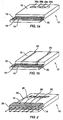
- Block 10 is provided with a stepped portion 12.
- stepped portion 12 is dimensioned such that the height of the step is chosen to be substantially equal to half the height of a laser diode emitter bar.
- the stepped portion 12 of carrier 12 is adapted to receive a laser diode bar.
- Stepped portion 12 has a mounting face 14 thereon for mounting a laser diode bar thereto.
- Carrier 10 also includes a mating face 16.
- carrier 10 When carrier 10 is formed from diamond, it can be formed as a rectangular block and the step may be etched using a process such as masked plasma etching or other well known techniques. Alternatively, carrier 10 may be formed in several ways which incorporate the step feature, such as by consolidation of particulate diamond in a preform which incorporates the step features disclosed in pending application serial No. 07/704,997, filed February 28, 1991, or by performing a diamond growth process on a substrate, such as silicon, which incorporates a negative image of the step feature.
- the present invention permits improved alignment of the laser bars (an important parameter), due to the enhanced precision with which the mounting surfaces can be fabricated and the resulting precision with which the laser diode array bars can be mated to those mounting surfaces.
- Metallization patterns can be more advantageously fabricated to connect the laser diode arrays in parallel, series, or any combination thereof.
- the present method lends itself to distribution of power to individual diodes, making possible compensation for individual diode variation, and enabling phase or frequency modulation.
Landscapes
- Physics & Mathematics (AREA)
- Condensed Matter Physics & Semiconductors (AREA)
- General Physics & Mathematics (AREA)
- Electromagnetism (AREA)
- Optics & Photonics (AREA)
- Semiconductor Lasers (AREA)
Claims (5)
- Laserdiodenstreifen (26) und Montagebaugruppe (30) dafür, die aufweist:einen ersten Träger (10a) und einen zweiten Träger (10b), die jeweils aufweisen:einen allgemein rechtwinklig geformten Block (10) aus dielektrischem Material hoher Wärmeleitfähigkeit, der an seiner ersten Seite einen gestuften Ausschnitt (12) hat, dessen Höhe im wesentlichen gleich der Hälfte der Höhe des Laserdiodenstreifens (26) ist und auf dem eine Montagestirnfläche (14a, 14b) gebildet ist, undLaserdiodenkontaktglieder (18) zur Herstellung elektrischen Kontakts mit Laserdiodenemittern des auf dem Träger zu montierenden Laserdiodenstreifens;der erste Träger hat außerdem eine Paßfläche (16a) auf seiner die Montagestirnfläche (14a) aufweisenden ersten Seite und eine Kopplungsfläche (32) auf einer der ersten Seite gegenüberliegenden zweiten Seite;der zweite Träger hat außerdem eine Paßfläche (16b) auf seiner die Montagestirnfläche (14b) aufweisenden ersten Seite und eine Kopplungsfläche (32) auf einer dieser ersten Seite gegenüberliegenden zweiten Seite;die Paßflächen (16a, 16b) des ersten und zweiten Trägers sind miteinander durch ein Verbindungsmaterial hoher Wärmeleitfähigkeit verbunden, wobei der erste und zweite Träger so ausgerichtet sind, daß ihre gestuften Ausschnitte einander gegenüberliegen und zwischen ihren Montagestirnflächen einen Laserdiodenhohlraum bilden; undder Laserdiodenstreifen (26) ist in dem Laserdiodenhohlraum angeordnet und mit den Montagestirnflächen (14a, 14b) des ersten und zweiten Trägers mittels eines Verbindungsmaterials hoher Wärmeleitfähigkeit verbunden.
- Baugruppe, die wenigstens zwei Laserdiodenmontagebaugruppen (30) gemäß Anspruch 1 aufweist, bei denen eine Kopplungsfläche (32) entweder des ersten (10a) oder des zweiten Trägers (10b) einer ersten dieser beiden Montagebaugruppen (30) mit einer Kopplungsfläche (32) eines ersten (10c) oder zweiten Trägers (10d) der zweiten der beiden Montagebaugruppen (30) verbunden ist.
- Baugruppe nach Anspruch 1 oder 2, bei denen die oder ein erster und/oder zweiter Träger aus Berylliumoxid gebildet sind bzw. ist.
- Baugruppe nach Anspruch 1 oder 2, bei der die oder ein erster und/oder zweiter Träger aus Diamant gebildet sind bzw. ist.
- Baugruppe nach einem der vorangehenden Ansprüche, bei der die oder ein Laserdiodenstreifen elektrische Anschlüsse in Kontakt mit den Kontaktgliedern (18) des ersten und/oder zweiten Trägers hat bzw. haben.
Applications Claiming Priority (2)
| Application Number | Priority Date | Filing Date | Title |
|---|---|---|---|
| US07/818,286 US5325384A (en) | 1992-01-09 | 1992-01-09 | Structure and method for mounting laser diode arrays |
| US818286 | 1992-01-09 |
Publications (2)
| Publication Number | Publication Date |
|---|---|
| EP0550996A1 EP0550996A1 (de) | 1993-07-14 |
| EP0550996B1 true EP0550996B1 (de) | 1997-08-06 |
Family
ID=25225158
Family Applications (1)
| Application Number | Title | Priority Date | Filing Date |
|---|---|---|---|
| EP92311616A Expired - Lifetime EP0550996B1 (de) | 1992-01-09 | 1992-12-18 | Bausatz für einen Laserdiodenblock |
Country Status (4)
| Country | Link |
|---|---|
| US (1) | US5325384A (de) |
| EP (1) | EP0550996B1 (de) |
| JP (1) | JPH0613717A (de) |
| DE (1) | DE69221458T2 (de) |
Cited By (5)
| Publication number | Priority date | Publication date | Assignee | Title |
|---|---|---|---|---|
| US7305016B2 (en) | 2005-03-10 | 2007-12-04 | Northrop Grumman Corporation | Laser diode package with an internal fluid cooling channel |
| US7656915B2 (en) | 2006-07-26 | 2010-02-02 | Northrop Grumman Space & Missions Systems Corp. | Microchannel cooler for high efficiency laser diode heat extraction |
| US8345720B2 (en) | 2009-07-28 | 2013-01-01 | Northrop Grumman Systems Corp. | Laser diode ceramic cooler having circuitry for control and feedback of laser diode performance |
| US8937976B2 (en) | 2012-08-15 | 2015-01-20 | Northrop Grumman Systems Corp. | Tunable system for generating an optical pulse based on a double-pass semiconductor optical amplifier |
| US9590388B2 (en) | 2011-01-11 | 2017-03-07 | Northrop Grumman Systems Corp. | Microchannel cooler for a single laser diode emitter based system |
Families Citing this family (61)
| Publication number | Priority date | Publication date | Assignee | Title |
|---|---|---|---|---|
| US5394426A (en) * | 1992-11-13 | 1995-02-28 | Hughes Aircraft Company | Diode laser bar assembly |
| US5548608A (en) * | 1993-02-08 | 1996-08-20 | Zhang; Tong | Laser head and telescopic cavity for diode-pumped solid-state lasers |
| US5422901A (en) * | 1993-11-15 | 1995-06-06 | Motorola, Inc. | Semiconductor device with high heat conductivity |
| US5764675A (en) * | 1994-06-30 | 1998-06-09 | Juhala; Roland E. | Diode laser array |
| US5898211A (en) * | 1996-04-30 | 1999-04-27 | Cutting Edge Optronics, Inc. | Laser diode package with heat sink |
| US5743901A (en) | 1996-05-15 | 1998-04-28 | Star Medical Technologies, Inc. | High fluence diode laser device and method for the fabrication and use thereof |
| US5748654A (en) * | 1996-06-17 | 1998-05-05 | Trw Inc. | Diode array providing either a pulsed or a CW mode of operation of a diode pumped solid state laser |
| US5734672A (en) | 1996-08-06 | 1998-03-31 | Cutting Edge Optronics, Inc. | Smart laser diode array assembly and operating method using same |
| US5715264A (en) * | 1996-09-12 | 1998-02-03 | Opto Power Corporation | Laser diode array |
| US5923692A (en) * | 1996-10-24 | 1999-07-13 | Sdl, Inc. | No wire bond plate (NWBP) packaging architecture for two dimensional stacked diode laser arrays |
| JP3816194B2 (ja) * | 1996-11-22 | 2006-08-30 | ファナック株式会社 | 冷却装置、光源装置、面発光装置、およびその製造方法 |
| US5909458A (en) * | 1996-11-27 | 1999-06-01 | The Regents Of The University Of California | Low-cost laser diode array |
| US6240116B1 (en) | 1997-08-14 | 2001-05-29 | Sdl, Inc. | Laser diode array assemblies with optimized brightness conservation |
| US5917704A (en) * | 1997-10-06 | 1999-06-29 | Ford Motor Company | Laser-solderable electronic component |
| US6295307B1 (en) * | 1997-10-14 | 2001-09-25 | Decade Products, Inc. | Laser diode assembly |
| US5995289A (en) | 1997-12-15 | 1999-11-30 | The University Of Utah Research Foundation | Laser beam coupler, shaper and collimator |
| US6259713B1 (en) | 1997-12-15 | 2001-07-10 | The University Of Utah Research Foundation | Laser beam coupler, shaper and collimator device |
| US6045321A (en) * | 1998-03-23 | 2000-04-04 | Lucent Technologies, Inc. | Method and apparatus for transporting laser bars |
| US5913108A (en) * | 1998-04-30 | 1999-06-15 | Cutting Edge Optronics, Inc. | Laser diode packaging |
| US5989932A (en) * | 1998-07-28 | 1999-11-23 | Lucent Technologies, Inc. | Method and apparatus for retaining and releasing laser bars during a facet coating operation |
| US6744800B1 (en) * | 1998-12-30 | 2004-06-01 | Xerox Corporation | Method and structure for nitride based laser diode arrays on an insulating substrate |
| US6636538B1 (en) * | 1999-03-29 | 2003-10-21 | Cutting Edge Optronics, Inc. | Laser diode packaging |
| US6385220B1 (en) | 1999-04-21 | 2002-05-07 | Gsi Lumonics Inc. | Laser clamping assembly and method |
| CA2284946A1 (en) | 1999-10-04 | 2001-04-04 | Institut National D'optique | Laser diode array assembly made from a ridged monolithic substrate |
| DE10018043A1 (de) * | 2000-04-07 | 2001-10-11 | Jenoptik Jena Gmbh | Verfahren zur Kontaktierung eines Hochleistungsdiodenlaserbarrens und eine Hochleistungsdiodenlaserbarren-Kontakt-Anordnung von elektrischen Kontakten thermisch untergeordneter Funktion |
| DE10036283A1 (de) * | 2000-07-26 | 2002-02-07 | Bosch Gmbh Robert | Laserdiodenanordnung |
| JP2002151781A (ja) * | 2000-11-10 | 2002-05-24 | Mitsubishi Electric Corp | 光素子モジュール |
| JP2002232061A (ja) * | 2001-02-01 | 2002-08-16 | Mitsubishi Electric Corp | 半導体レーザ装置の製造方法および半導体レーザ装置 |
| US6700913B2 (en) * | 2001-05-29 | 2004-03-02 | Northrop Grumman Corporation | Low cost high integrity diode laser array |
| US6853007B2 (en) | 2001-12-28 | 2005-02-08 | Finisar Corporation | Submount for vertical cavity surface emitting lasers and detectors |
| US6927086B2 (en) * | 2002-09-24 | 2005-08-09 | Decade Products, Inc. | Method and apparatus for laser diode assembly and array |
| US7170919B2 (en) * | 2003-06-23 | 2007-01-30 | Northrop Grumman Corporation | Diode-pumped solid-state laser gain module |
| US7495848B2 (en) * | 2003-07-24 | 2009-02-24 | Northrop Grumman Corporation | Cast laser optical bench |
| US7586962B1 (en) * | 2004-03-29 | 2009-09-08 | The United States Of America As Represented By The Secretary Of The Air Force | Integrated diamond carrier for laser bar arrays |
| US7352785B2 (en) * | 2004-04-30 | 2008-04-01 | Richard L. Fork | Solid state laser medium and laser medium heat transfer method |
| JP2006013038A (ja) * | 2004-06-24 | 2006-01-12 | Mitsubishi Electric Corp | 半導体レーザアレイ装置 |
| US20060045158A1 (en) * | 2004-08-30 | 2006-03-02 | Chian Chiu Li | Stack-type Wavelength-tunable Laser Source |
| US7529286B2 (en) * | 2005-12-09 | 2009-05-05 | D-Diode Llc | Scalable thermally efficient pump diode systems |
| EP1811617A1 (de) * | 2006-01-18 | 2007-07-25 | JENOPTIK Laserdiode GmbH | Träger für eine vertikale Anordnung von Laserdiodenbarren mit Anschlag |
| USD570506S1 (en) * | 2006-06-20 | 2008-06-03 | Matsushita Electric Industrial Co., Ltd. | Lighting apparatus |
| EP2050145A4 (de) * | 2006-07-28 | 2009-09-02 | Koninkl Philips Electronics Nv | Lichtquelle mit kantenemittierenden elementen |
| US7864825B2 (en) * | 2006-08-10 | 2011-01-04 | Lasertel, Inc. | Method and system for a laser diode bar array assembly |
| DE102006039396A1 (de) * | 2006-08-22 | 2008-03-13 | Robert Bosch Gmbh | Laserlichtquelle |
| US20080056314A1 (en) * | 2006-08-31 | 2008-03-06 | Northrop Grumman Corporation | High-power laser-diode package system |
| US7724791B2 (en) * | 2008-01-18 | 2010-05-25 | Northrop Grumman Systems Corporation | Method of manufacturing laser diode packages and arrays |
| DE102008026229B4 (de) * | 2008-05-29 | 2012-12-27 | Jenoptik Laser Gmbh | Wärmeübertragungsvorrichtung zur doppelseitigen Kühlung eines Halbleiterbauelementes |
| DE102008026801B4 (de) | 2008-06-02 | 2012-05-31 | Jenoptik Laser Gmbh | Wärmeübertragungsvorrichtung zur doppelseitigen Kühlung eines Halbleiterbauelementes und Verfahren zu seiner Montage |
| DE102008036439A1 (de) * | 2008-08-05 | 2010-02-11 | Jenoptik Laserdiode Gmbh | Wärmeableitmodul mit einem Halbleiterelement und Herstellungsverfahren für ein solches Wärmeableitmodul |
| DE102009009521A1 (de) * | 2009-02-18 | 2010-08-19 | Osram Opto Semiconductors Gmbh | Halbleiterlaser und Verfahren zur Herstellung eines Halbleiterlasers |
| US8220140B1 (en) | 2010-09-13 | 2012-07-17 | Western Digital (Fremont), Llc | System for performing bonding a first substrate to a second substrate |
| US8518814B2 (en) | 2011-12-02 | 2013-08-27 | Northrop Grumman Systems Corporation | Methods of fabrication of high-density laser diode stacks |
| JP2013211303A (ja) * | 2012-03-30 | 2013-10-10 | Ushio Inc | 半導体レーザ装置 |
| JP6500342B2 (ja) * | 2013-04-27 | 2019-04-17 | 日亜化学工業株式会社 | 半導体レーザ装置の製造方法並びにサブマウントの製造方法 |
| US10431955B2 (en) * | 2014-04-25 | 2019-10-01 | Lmd Power Of Light Corp | Laser core having conductive mass electrical connection |
| US11025031B2 (en) | 2016-11-29 | 2021-06-01 | Leonardo Electronics Us Inc. | Dual junction fiber-coupled laser diode and related methods |
| US11406004B2 (en) | 2018-08-13 | 2022-08-02 | Leonardo Electronics Us Inc. | Use of metal-core printed circuit board (PCB) for generation of ultra-narrow, high-current pulse driver |
| US11056854B2 (en) | 2018-08-14 | 2021-07-06 | Leonardo Electronics Us Inc. | Laser assembly and related methods |
| US11296481B2 (en) | 2019-01-09 | 2022-04-05 | Leonardo Electronics Us Inc. | Divergence reshaping array |
| US11752571B1 (en) | 2019-06-07 | 2023-09-12 | Leonardo Electronics Us Inc. | Coherent beam coupler |
| EP3792683A1 (de) | 2019-09-16 | 2021-03-17 | Leonardo Electronics US Inc. | Hexagonaler homogenisator mit asymmetrischer eingangsintensität |
| WO2023074182A1 (ja) * | 2021-10-27 | 2023-05-04 | パナソニックホールディングス株式会社 | 発光装置、レーザー加工システム、発光装置の製造方法、及び、レーザー加工システムの製造方法 |
Family Cites Families (7)
| Publication number | Priority date | Publication date | Assignee | Title |
|---|---|---|---|---|
| USB411062I5 (de) * | 1964-11-13 | |||
| US3590248A (en) * | 1965-04-13 | 1971-06-29 | Massachusetts Inst Technology | Laser arrays |
| US3303432A (en) * | 1966-04-18 | 1967-02-07 | Gen Electric | High power semiconductor laser devices |
| US4315225A (en) * | 1979-08-24 | 1982-02-09 | Mcdonnell Douglas Corporation | Heat sink laser diode array |
| US4716568A (en) * | 1985-05-07 | 1987-12-29 | Spectra Diode Laboratories, Inc. | Stacked diode laser array assembly |
| US4719631A (en) * | 1986-01-10 | 1988-01-12 | The United States Of America As Represented By The Secretary Of The Air Force | Conductively cooled laser diode array pumped laser |
| US5099488A (en) * | 1991-03-27 | 1992-03-24 | Spectra Diode Laboratories, Inc. | Ribbed submounts for two dimensional stacked laser array |
-
1992
- 1992-01-09 US US07/818,286 patent/US5325384A/en not_active Expired - Fee Related
- 1992-12-18 DE DE69221458T patent/DE69221458T2/de not_active Expired - Fee Related
- 1992-12-18 EP EP92311616A patent/EP0550996B1/de not_active Expired - Lifetime
-
1993
- 1993-01-08 JP JP5018059A patent/JPH0613717A/ja active Pending
Cited By (8)
| Publication number | Priority date | Publication date | Assignee | Title |
|---|---|---|---|---|
| US7305016B2 (en) | 2005-03-10 | 2007-12-04 | Northrop Grumman Corporation | Laser diode package with an internal fluid cooling channel |
| US7466732B2 (en) | 2005-03-10 | 2008-12-16 | Northrop Grumman Corporation | Laser diode package with an internal fluid cooling channel |
| US7656915B2 (en) | 2006-07-26 | 2010-02-02 | Northrop Grumman Space & Missions Systems Corp. | Microchannel cooler for high efficiency laser diode heat extraction |
| US7957439B2 (en) | 2006-07-26 | 2011-06-07 | Northrop Grumman Space & Missions | Microchannel cooler for high efficiency laser diode heat extraction |
| US8345720B2 (en) | 2009-07-28 | 2013-01-01 | Northrop Grumman Systems Corp. | Laser diode ceramic cooler having circuitry for control and feedback of laser diode performance |
| US9590388B2 (en) | 2011-01-11 | 2017-03-07 | Northrop Grumman Systems Corp. | Microchannel cooler for a single laser diode emitter based system |
| US8937976B2 (en) | 2012-08-15 | 2015-01-20 | Northrop Grumman Systems Corp. | Tunable system for generating an optical pulse based on a double-pass semiconductor optical amplifier |
| US9276375B2 (en) | 2012-08-15 | 2016-03-01 | Northrop Grumman Systems Corp. | Tunable system for generating an optical pulse based on a double-pass semiconductor optical amplifier |
Also Published As
| Publication number | Publication date |
|---|---|
| JPH0613717A (ja) | 1994-01-21 |
| DE69221458T2 (de) | 1997-12-11 |
| EP0550996A1 (de) | 1993-07-14 |
| DE69221458D1 (de) | 1997-09-11 |
| US5325384A (en) | 1994-06-28 |
Similar Documents
| Publication | Publication Date | Title |
|---|---|---|
| US5325384A (en) | Structure and method for mounting laser diode arrays | |
| US5913108A (en) | Laser diode packaging | |
| US5985684A (en) | Process for manufacturing a laser diode having a heat sink | |
| US5394426A (en) | Diode laser bar assembly | |
| US4315225A (en) | Heat sink laser diode array | |
| EP1365488B1 (de) | Verfahren zum Verpacken einer Subträgerbaugruppe | |
| EP0891630B1 (de) | Gehäuse für laserdiodenreihe | |
| US5305344A (en) | Laser diode array | |
| US5105430A (en) | Thin planar package for cooling an array of edge-emitting laser diodes | |
| US5848083A (en) | Expansion-matched high-thermal-conductivity stress-relieved mounting modules | |
| US5311530A (en) | Semiconductor laser array | |
| US6826916B2 (en) | Laser module, Peltier module, and Peltier module integrated heat spreader | |
| US4393393A (en) | Laser diode with double sided heat sink | |
| US6101206A (en) | Laser-diode device including heat-conducting walls, semiconductor strips and isolating seals and process for making laser-diode device | |
| US5923692A (en) | No wire bond plate (NWBP) packaging architecture for two dimensional stacked diode laser arrays | |
| EP3159981A1 (de) | Thermisch leitendes, stromführendes, elektrisch isoliertes submount für laserdioden-arrays | |
| JPH11145561A (ja) | 光半導体モジュール | |
| US20020172244A1 (en) | Self-separating laser diode assembly and method | |
| CN110556705A (zh) | 激光二极体表面安装结构 | |
| US11557874B2 (en) | Double-sided cooling of laser diodes | |
| JPH036875A (ja) | 半導体レーザ | |
| JPH09148675A (ja) | 光モジュールの実装構造 | |
| US20060262819A1 (en) | Diode laser component with an integrated cooling element | |
| RU2119704C1 (ru) | Полупроводниковый лазер | |
| KR102882272B1 (ko) | 세라믹 기판 제조방법 |
Legal Events
| Date | Code | Title | Description |
|---|---|---|---|
| PUAI | Public reference made under article 153(3) epc to a published international application that has entered the european phase |
Free format text: ORIGINAL CODE: 0009012 |
|
| AK | Designated contracting states |
Kind code of ref document: A1 Designated state(s): CH DE ES FR GB IT LI NL SE |
|
| 17P | Request for examination filed |
Effective date: 19940301 |
|
| 17Q | First examination report despatched |
Effective date: 19941005 |
|
| GRAG | Despatch of communication of intention to grant |
Free format text: ORIGINAL CODE: EPIDOS AGRA |
|
| GRAH | Despatch of communication of intention to grant a patent |
Free format text: ORIGINAL CODE: EPIDOS IGRA |
|
| GRAH | Despatch of communication of intention to grant a patent |
Free format text: ORIGINAL CODE: EPIDOS IGRA |
|
| GRAA | (expected) grant |
Free format text: ORIGINAL CODE: 0009210 |
|
| AK | Designated contracting states |
Kind code of ref document: B1 Designated state(s): CH DE ES FR GB IT LI NL SE |
|
| PG25 | Lapsed in a contracting state [announced via postgrant information from national office to epo] |
Ref country code: NL Free format text: LAPSE BECAUSE OF FAILURE TO SUBMIT A TRANSLATION OF THE DESCRIPTION OR TO PAY THE FEE WITHIN THE PRESCRIBED TIME-LIMIT Effective date: 19970806 Ref country code: LI Effective date: 19970806 Ref country code: IT Free format text: LAPSE BECAUSE OF FAILURE TO SUBMIT A TRANSLATION OF THE DESCRIPTION OR TO PAY THE FEE WITHIN THE PRE;WARNING: LAPSES OF ITALIAN PATENTS WITH EFFECTIVE DATE BEFORE 2007 MAY HAVE OCCURRED AT ANY TIME BEFORE 2007. THE CORRECT EFFECTIVE DATE MAY BE DIFFERENT FROM THE ONE RECORDED.SCRIBED TIME-LIMIT Effective date: 19970806 Ref country code: ES Free format text: THE PATENT HAS BEEN ANNULLED BY A DECISION OF A NATIONAL AUTHORITY Effective date: 19970806 Ref country code: CH Effective date: 19970806 |
|
| REG | Reference to a national code |
Ref country code: CH Ref legal event code: EP |
|
| ET | Fr: translation filed | ||
| REF | Corresponds to: |
Ref document number: 69221458 Country of ref document: DE Date of ref document: 19970911 |
|
| PG25 | Lapsed in a contracting state [announced via postgrant information from national office to epo] |
Ref country code: SE Effective date: 19971106 |
|
| NLV1 | Nl: lapsed or annulled due to failure to fulfill the requirements of art. 29p and 29m of the patents act | ||
| REG | Reference to a national code |
Ref country code: CH Ref legal event code: PL |
|
| PLBE | No opposition filed within time limit |
Free format text: ORIGINAL CODE: 0009261 |
|
| STAA | Information on the status of an ep patent application or granted ep patent |
Free format text: STATUS: NO OPPOSITION FILED WITHIN TIME LIMIT |
|
| 26N | No opposition filed | ||
| REG | Reference to a national code |
Ref country code: GB Ref legal event code: IF02 |
|
| PGFP | Annual fee paid to national office [announced via postgrant information from national office to epo] |
Ref country code: GB Payment date: 20031105 Year of fee payment: 12 |
|
| PGFP | Annual fee paid to national office [announced via postgrant information from national office to epo] |
Ref country code: FR Payment date: 20031201 Year of fee payment: 12 |
|
| PGFP | Annual fee paid to national office [announced via postgrant information from national office to epo] |
Ref country code: DE Payment date: 20031230 Year of fee payment: 12 |
|
| PG25 | Lapsed in a contracting state [announced via postgrant information from national office to epo] |
Ref country code: GB Free format text: LAPSE BECAUSE OF NON-PAYMENT OF DUE FEES Effective date: 20041218 |
|
| PG25 | Lapsed in a contracting state [announced via postgrant information from national office to epo] |
Ref country code: DE Free format text: LAPSE BECAUSE OF NON-PAYMENT OF DUE FEES Effective date: 20050701 |
|
| GBPC | Gb: european patent ceased through non-payment of renewal fee |
Effective date: 20041218 |
|
| PG25 | Lapsed in a contracting state [announced via postgrant information from national office to epo] |
Ref country code: FR Free format text: LAPSE BECAUSE OF NON-PAYMENT OF DUE FEES Effective date: 20050831 |
|
| REG | Reference to a national code |
Ref country code: FR Ref legal event code: ST |