EP0552507A1 - Arbitre avec un signal direct qui est modifiable sous contrôle des conflits de priorité - Google Patents
Arbitre avec un signal direct qui est modifiable sous contrôle des conflits de priorité Download PDFInfo
- Publication number
- EP0552507A1 EP0552507A1 EP92203663A EP92203663A EP0552507A1 EP 0552507 A1 EP0552507 A1 EP 0552507A1 EP 92203663 A EP92203663 A EP 92203663A EP 92203663 A EP92203663 A EP 92203663A EP 0552507 A1 EP0552507 A1 EP 0552507A1
- Authority
- EP
- European Patent Office
- Prior art keywords
- input
- arbiter
- signals
- section
- priority
- Prior art date
- Legal status (The legal status is an assumption and is not a legal conclusion. Google has not performed a legal analysis and makes no representation as to the accuracy of the status listed.)
- Granted
Links
Images


Classifications
-
- G—PHYSICS
- G06—COMPUTING OR CALCULATING; COUNTING
- G06F—ELECTRIC DIGITAL DATA PROCESSING
- G06F13/00—Interconnection of, or transfer of information or other signals between, memories, input/output devices or central processing units
- G06F13/14—Handling requests for interconnection or transfer
-
- H—ELECTRICITY
- H04—ELECTRIC COMMUNICATION TECHNIQUE
- H04L—TRANSMISSION OF DIGITAL INFORMATION, e.g. TELEGRAPHIC COMMUNICATION
- H04L1/00—Arrangements for detecting or preventing errors in the information received
Definitions
- the invention relates to a arbiter for providing at an arbiter output an absolute priority signal associated with a particular one of a plurality of input signals received at an arbiter input.
- the invention relates in particular to an asynchronous arbiter.
- An arbiter is a well known interface circuit that controls a communication protocol on the basis of assigning priority to a particular input signal selected from a plurality of input signals in order to determine a processing sequence for the input signals.
- the priority assignment may be based on temporal aspects of the signals, e.g., the order of arrivals at the arbiter's inputs.
- Assigning a priority to a particular one of the input signals is then to be understood as selecting the particular input signal on the basis of its temporal characteristics with respect to the temporal characteristics of the other input signals: e.g., the particular input signal is the first to have arrived and determines the further processing.
- arbiters are used for controlling the communication between transmitting stations and receiving stations interconnected via a bus system.
- U.S. Patent 4,835,422 issued to Dike et al. discusses a electronic arbiter circuit with an input section that provides relative priority signals upon receiving a plurality of input signals. Each respective relative priority signal specifies which one of a respective pair of input signals has gained priority over the other input signal.
- the relative priority signals associated with all pairs of input signals are supplied to a decode logic circuit.
- the decode logic circuit operates on the relative priority signals in order to furnish output signals specifying an absolute priority of a particular one of the input signals. That is, the output signals indicate which one of the input signals is considered to have gained priority over all other input signals.
- the decode logic circuit takes care of priority conflicts that may occur at the level of the relative priority signals.
- a priority conflict is an event wherein, for example, three or more input signals arrive substantially simultaneously within the resolution of the electronics and the delay paths involved. Such an event gives rise to inconsistences.
- the relative priority signals may indicate that the respective input signals at first, second and third input terminals respectively gained priority over the input signals at the second, third and first input terminals. Assuming that one of these input signals indeed was the first to arrive overall, such a cyclic relationship does not give a unambiguous absolute priority winner.
- the decode logic circuit is designed to resolve the conflict by selecting in a predetermined manner one of the input signals, which was involved in causing the conflict, as the absolute priority winner.
- the signal path is from the inputs of the input section through the decode logic circuit to the circuit's outputs.
- the decode logic circuit itself comprises arrangements of several logic AND gates that receive particular combinations of the relative priority signals to be fed into a single logic OR gate.
- the size of each AND gate and each OR gate grows with the number of relative priority signals to be processed.
- 4-input arbiter for instance, four arrangements of three 3-input AND gates with outputs coupled to a 3-input OR gate each are required.
- a 6-input arbiter designed on the basis of the same philosophy would need four arrangements with twelve 5-input AND gates ad a 12-input OR gate each, and two arrangements with eleven 5-input AND gates and an eleven-input OR gate each.
- the output signals which are indicative of the absolute priority of a particular input signal, may change if one or more input signals, other than the particular input signal, switch. Both switching of an input signal with a lower priority and the operation of the decode logic will resolve a priority conflict. Switching of a lower priority signal may change the status of the decode logic and, therefore, the output signals.
- the invention provides an arbiter for providing at an arbiter output an absolute priority signal associated with a particular one of a plurality of input signals at an arbiter input gaining priority over all other input signals.
- the arbiter comprises a signal processing path between the arbiter input and the arbiter output for determining the absolute priority signal on the basis of the input signals.
- the arbiter further comprises control means coupled to the signal path for detecting a priority conflict and for thereupon generating control signals for modifying the signal path in order to resolve the conflict.
- the invention provides an architecture wherein the conflict-resolving circuitry is located outside the main signal path that couples the input to the output.
- the control means interferes with the priority assignment process only in case of an occasional conflict.
- the control means comprises the conflict-resolving but delay-generating devices. As a result, the delay in the signal path is largely independent of the number of input signals to be processed.
- Fig. 1 shows a known arbiter.
- the arbiter includes an input 10 for receiving input signals S1-S N , an input portion 12 for correlating pairs of input signals S i ,S j (i ⁇ j) in order to generate relative priority signals R1-R M , wherein M equals N(N-1)/2.
- Each one of the relative priority signals R1-R M indicates which one of the input signals of the associated pair has gained priority over the other one.
- the arbiter further includes a decode logic section 14 for providing absolute priority signals G1-G N at an output 16. Absolute priority signals G1-G N specify which one of input signals S1-S N has gained priority over all other ones.
- Decode logic section 14 resolves the priority conflicts (see above) that may arise when, for instance, input portion 12 supplies contradictory relative priority signals R1-R M or when three or more of the input signals S1-S N arrive substantially simultaneously. In case of such a conflict, decode logic section 14 settles into an unambiguous state and provides predetermined and unique absolute priority signals G1-G N at output 16.
- Decode logic section 14 generally includes a hierarchy of logic gates whose sizes scale according to the number of relative priority signals R1-R M to be processed. As a consequence, the delays caused by a succession of logic gates will be more pronounced when the number of relative priority signals R1-R M to be processed is increased.
- Fig. 2 shows a first example of the arbiter in accordance with the invention.
- the arbiter includes input terminals 20 for receiving input signals S1-S N , and an input section 22 for generating relative priority signals R1-R M .
- Relative priority signals R1-R M each specify a relative priority within a respective subset (e.g. pair or quadruplet) of input signals S1-S N . That is, each particular relative priority signal indicates which one of the input signals within a particular subset has gained priority over the other input signals in the same subset.
- the arbiter has an output section 24 that furnishes absolute priority signals G1-G N at an output 26 in response to relative priority signals R1-R M .
- the signal processing from input 20 via input section 22 through output section 24 to output 26 constitutes a direct signal path.
- a typical value of the signal propagation delay in the direct path of the arbiter in the invention is 5.5 nsec.
- the arbiter comprises a control section 28 that receives relative priority signals R1-R M and provides control signals C1-C K to input section 22 in the event of a priority conflict.
- Control signals C1-C K resolve the conflict by forcing input section 22 to supply conflict-free relative priority signals R1-R M .
- the processing of input signals S1-S N via control section 28 constitutes a second signal path.
- Control section 28 solves the priority conflict by modifying the direct signal path. As mentioned above, the second signal path is only used occasionally. Since control section 28 constitutes additional circuitry, it is therefore in general advantageous to keep this circuitry out of the direct path. It is in control section 28 that gate delays become noticeable when the number of relative priority signals R1-R M to be processed is increased.
- Fig. 3 shows a second example of an arbiter in the invention, using the functional arrangement of Fig. 2 and parts similar to those of the prior art arbiter in Fig. 1.
- input portion 12 and decode logic section 14 together form a known priority arbiter embedded in the architecture of the invention.
- Decode logic section 14 takes care of occasional priority conflicts in the usual way.
- control signals C1-C K from decode logic 14 are supplied to a transfer section 30.
- Transfer section 30 controls the routing of input signals S1-S N to input portion 12 in response to control signals C1-C K in case of a priority conflict.
- transfer section 30 supplies to input portion 12 a combination of control signals C1-C K and input signals S1-S N that removes the conflict and creates unambiguous absolute priority signals G1-G N . If there is no conflict, control signals C1-C K do not interfere with input signals S1-S N propagating from input 20 to input portion 12. That is, transfer section 30 is maintained transparent to input signals S1-S N .
- Fig. 4 gives a first detailed version of a 4-input arbiter according to the invention.
- the architecture of Fig. 3 is used.
- Input portion 12 comprises six mutual-exclusive elements 40-50 for evaluating particular pairs of input signals S1, S2, S3 and S4 to generate relative priority signals R1-R12.
- Relative priority signals R1-R12 are supplied to inputs of decode logic section 14.
- decode logic section 14 is a combinatorial arrangement of logic gates. That is, control signals C1-C4 provided by decode logic section 14 are determined by the momentary values of relative priority signals R1-R12.
- control signals C1-C4 provided by decode logic section 14 are determined by the momentary values of relative priority signals R1-R12.
- the leads between element 40, which receives input signals S1 and S2, and decode logic section 14 are denoted by 1/2 and 2/1, indicating the connections for relative priority signals R1: "S1 beats S2" and R2: “S2 beats S1", respectively. Similar notations are used for the leads between the other elements 42-50 ad decode logic section 14.
- Decode logic section 14 provides transfer section 30 with control signals C1-C4 that specify a conflict-free overall (absolute) priority situation.
- Transfer section 30 includes logic OR gates 70-84 that transfer input signals S1, S2, S3 and S4 to mutual-exclusive elements 42-48 in response to control signals C1-C4.
- Elements 40-50 are directly connected to output section 24.
- Output section 24 comprises four logic AND gates 90-96 for supplying absolute priority signals G1-G4. Each of AND gates 90-96 has inputs connected to selected ones of outputs a and b of mutual-exclusive elements 40-50.
- Each of mutual exclusive elements 40-50 includes a sequential logic circuit. That is, each of elements 40-50 furnishes output signals that depend on both the momentary and previous values of the signals received by the element.
- the design of each of element 40-50 is such that both element outputs a and b provide a logic LOW when the signals at element inputs c and d both are HIGH. If the signal at input c goes LOW first, output a provides a HIGH and output b provides a LOW, and vice versa if input d goes LOW first. In case the signal at the other input (d or c, respectively) thereupon goes LOW as well, the signals at outputs a and b do not change.
- decode logic section 14 develops the following values for control signals C1-C4: C1 is HIGH, and C2-C4 all are LOW.
- Control signals C1-C4 are supplied to OR gates 70-84 in transfer section 30.
- OR gates 72 and 76 both receive a HIGH from decode logic section 14. Accordingly, both input d of element 42 and input d of element 44 receive a HIGH, and both input c of element 42 and input c of element 44 receive a LOW.
- Element 42 does not change its output signals, but element 44 is forced to accept a new state, wherein output a is HIGH and output b is LOW.
- lead 1/4 now is HIGH and lead 4/1 is low.
- Decode logic section 14 retains its state, but output section 24 now provides absolute priority signals G1-G4 indicative of the priority assigned to S1, i.e., G1 is HIGH and G2-G4 all are LOW.
- the partitioning of the architecture into a direct signal path from input portion to output section 24 and a control path through decode logic section 14 preferably is used to optimize the components in the direct path with regard to speed.
- the components in the control path, particularly decode logic section 14, preferably are optimized with regard to power consumption and, in an integrated circuit embodiment, with regard to substrate area.
- Decode logic section 14 as represented in Fig. 4 is the same as used in a 4-input arbiter of the prior art.
- the shown architecture thus permits usage of known and available building blocks.
- AND gates 100-106 of decode logic section 14 may be left out since they do not contribute to the resolving of priority conflicts.
- removal of some of the logic gates from the decode logic section will affect the operation of the conflict-solving part and is therefore not recommended.
- Fig. 5 shows a second example of an arbiter according to the invention.
- the only difference from the arbiter of Fig. 4 is that output section 24 of Fig. 4 now has been merged with decode logic section 14. Since the logic operation in each of AND gates 100-106 is performed on the same combinations of relative priority signals R1-R12 as in AND gates 90-96 of Fig. 4, absolute priority signals G1-G4 are available at the respective outputs of AND gates 100-106.
- AND gates 100-106 do not contribute to the resolution of a priority conflict. Therefore, the connection between AND gates 100-106 and respective OR gates 108-114 may be deleted. Note also that, again, input section 12 and decode logic section 14, as drawn, together form a known arbiter. Operation of the arbiter is likewise identical to that of Fig. 4.
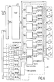
- Fig. 6 shows a third schematic example of an arbiter in accordance with the invention.
- the shown device is an 8-input arbiter for determining the absolute priority for input signals S1-S8.
- the architecture follows the general concept of Fig. 3 and need not be explained in further detail.
- Decode logic section 14 now has a particular structure based on partitioning of the decode circuitry into uniform decode logic blocks 200-210 and 220.
- Eight input signals S1-S8 give rise to fifty-six relative priority signals R1-R56 provided by twenty-eight mutual exclusive elements of input portion 12, similar to the operation in the arbiter of Fig. 4.
- Each one of the relative priority signals R1-R56 specifies the relative priority of one of the input signals S1-S8 over another.
- Relative priority signals R1-R56 are arranged in six groups of twelve relative priority signals each.
- Each respective one of decode logic blocks 200-220 receives a respective group of relative priority signals, now for determining a relative priority status within a respective quadruplet of input signals S1-S8.
- relative priority signals R1-R56 are divided into six groups relating to the priority statuses internal to the following quadruplets of input signals S1-S8: [S1-S2-S3-S4], [S1-S2-S5-S6], [S1-S2-S7-S8], [S3-S4-S5-S6], [S3-S4-S7-S8] and [S5-S6-S7-S8].
- Each respective group of relative priority signals is supplied to a respective one of decode logic blocks 200-210.
- Each of decode logic blocks 200-210 thereupon supplies further relative priority signals, now specifying the further relative priority status within the associated quadruplet of input signals.
- Logic OR gates 300-322 furnish output signals indicating in which pair of further relative priority signals there is an input signal that has priority over the input signals of the other pair within the same group.
- the pairs related to group [S3-S4-S7-S8] are [S3-S4] and [S7-S8].
- output signals are generated that indicate in which pair there is an input signal that has priority over the input signals of the other pairs in the same group.
- the respective OR gates are referred to by way of their respective output signals.
- OR gates 12/78 and 78/12 supply output signals, expressing that the relative priority within group [S1-S2-S7-S8] is either in pair S1/S2 or in pair S7/S8.
- Block 220 furnishes output signals that specify which one of all pairs is associated with the particular input signal that has the absolute priority. For example, lead 56/123478 is active, if the absolute priority should be assigned to either S5 or S6.
- the partitioning architecture has the advantage that any number of input signals can be dealt with by means of a hierarchical arrangement of layers with uniform decode blocks 200-220.
- An example of a circuit to be used as a decode block is decode section 14 in Fig. 4.
- the decode section's 14 design is simplified considerably in this way.
Landscapes
- Engineering & Computer Science (AREA)
- Theoretical Computer Science (AREA)
- Physics & Mathematics (AREA)
- General Engineering & Computer Science (AREA)
- General Physics & Mathematics (AREA)
- Computer Networks & Wireless Communication (AREA)
- Signal Processing (AREA)
- Bus Control (AREA)
- Data Exchanges In Wide-Area Networks (AREA)
- Facsimiles In General (AREA)
Applications Claiming Priority (2)
| Application Number | Priority Date | Filing Date | Title |
|---|---|---|---|
| US80425491A | 1991-12-04 | 1991-12-04 | |
| US804254 | 1991-12-04 |
Publications (2)
| Publication Number | Publication Date |
|---|---|
| EP0552507A1 true EP0552507A1 (fr) | 1993-07-28 |
| EP0552507B1 EP0552507B1 (fr) | 1998-02-11 |
Family
ID=25188543
Family Applications (1)
| Application Number | Title | Priority Date | Filing Date |
|---|---|---|---|
| EP92203663A Expired - Lifetime EP0552507B1 (fr) | 1991-12-04 | 1992-11-27 | Arbitre avec un signal direct qui est modifiable sous contrÔle des conflits de priorité |
Country Status (6)
| Country | Link |
|---|---|
| US (1) | US5546544A (fr) |
| EP (1) | EP0552507B1 (fr) |
| JP (1) | JPH05274246A (fr) |
| KR (1) | KR100263002B1 (fr) |
| DE (1) | DE69224427T2 (fr) |
| TW (1) | TW210416B (fr) |
Cited By (5)
| Publication number | Priority date | Publication date | Assignee | Title |
|---|---|---|---|---|
| WO2000000902A1 (fr) * | 1998-06-30 | 2000-01-06 | Sun Microsystems, Inc. | Arbitre asymetrique ayant un parcours de signal rapide |
| WO2001033375A1 (fr) * | 1999-11-03 | 2001-05-10 | Intel Corporation | Procede et appareil permettant de supporter la propagation multi-horloge dans un systeme informatique comportant un interface semi-duplex point-a-point |
| EP1164493A1 (fr) * | 2000-06-16 | 2001-12-19 | STMicroelectronics S.r.l. | Méthode d'arbitrage avec des priorités variables, par exemple pour des bus d'interconnexion, et système correspondant |
| US6842813B1 (en) | 2000-06-12 | 2005-01-11 | Intel Corporation | Method and apparatus for single wire signaling of request types in a computer system having a point to point half duplex interconnect |
| US6877052B1 (en) | 2000-09-29 | 2005-04-05 | Intel Corporation | System and method for improved half-duplex bus performance |
Families Citing this family (5)
| Publication number | Priority date | Publication date | Assignee | Title |
|---|---|---|---|---|
| FR2888349A1 (fr) * | 2005-07-06 | 2007-01-12 | St Microelectronics Sa | Adaptation de debit binaire dans un flot de traitement de donnees |
| KR100674994B1 (ko) * | 2005-09-10 | 2007-01-29 | 삼성전자주식회사 | 메모리 장치의 입력 버퍼와 메모리 제어장치 및 이를이용한 메모리 시스템 |
| US20100097131A1 (en) * | 2007-09-03 | 2010-04-22 | John Bainbridge | Hardening of self-timed circuits against glitches |
| US8892801B2 (en) * | 2012-05-23 | 2014-11-18 | Arm Limited | Arbitration circuity and method for arbitrating between a plurality of requests for access to a shared resource |
| CN107315703B (zh) * | 2017-05-17 | 2020-08-25 | 天津大学 | 双优先级控制型公平仲裁器 |
Citations (3)
| Publication number | Priority date | Publication date | Assignee | Title |
|---|---|---|---|---|
| US4251879A (en) * | 1979-05-02 | 1981-02-17 | Burroughs Corporation | Speed independent arbiter switch for digital communication networks |
| EP0334623A2 (fr) * | 1988-03-23 | 1989-09-27 | Du Pont Pixel Systems Limited | Système d'arbitrage |
| DE3917730A1 (de) * | 1989-05-31 | 1990-12-06 | Teldix Gmbh | Entscheidungslogik zur priorisierung und synchronisierung zeitlich asynchroner signale fuer hochgeschwindigkeits-anwendungen |
Family Cites Families (20)
| Publication number | Priority date | Publication date | Assignee | Title |
|---|---|---|---|---|
| US4016539A (en) * | 1973-09-12 | 1977-04-05 | Nippon Electric Company, Ltd. | Asynchronous arbiter |
| US4035780A (en) * | 1976-05-21 | 1977-07-12 | Honeywell Information Systems, Inc. | Priority interrupt logic circuits |
| US4449183A (en) * | 1979-07-09 | 1984-05-15 | Digital Equipment Corporation | Arbitration scheme for a multiported shared functional device for use in multiprocessing systems |
| NL7907179A (nl) * | 1979-09-27 | 1981-03-31 | Philips Nv | Signaalprocessorinrichting met voorwaardelijke- -interrupteenheid en multiprocessorsysteem met deze signaalprocessorinrichtingen. |
| US4402040A (en) * | 1980-09-24 | 1983-08-30 | Raytheon Company | Distributed bus arbitration method and apparatus |
| FR2494010B1 (fr) * | 1980-11-07 | 1986-09-19 | Thomson Csf Mat Tel | Dispositif d'arbitration decentralisee de plusieurs unites de traitement d'un systeme multiprocesseur |
| IT1193650B (it) * | 1983-01-31 | 1988-07-21 | Honeywell Inf Systems | Apparato di interruzione ad affidabilita' accresciuta |
| US4835672A (en) * | 1984-04-02 | 1989-05-30 | Unisys Corporation | Access lock apparatus for use with a high performance storage unit of a digital data processing system |
| US4612542A (en) * | 1984-12-20 | 1986-09-16 | Honeywell Inc. | Apparatus for arbitrating between a plurality of requestor elements |
| US4881195A (en) * | 1986-11-26 | 1989-11-14 | Rockwell International Corp. | Multi-requester arbitration circuit |
| IT1199745B (it) * | 1986-12-12 | 1988-12-30 | Honeywell Inf Systems | Circuito arbitratore di accesso |
| US4837682A (en) * | 1987-04-07 | 1989-06-06 | Glen Culler & Associates | Bus arbitration system and method |
| JPH073940B2 (ja) * | 1987-11-19 | 1995-01-18 | 三菱電機株式会社 | アービタ回路 |
| US4933901A (en) * | 1988-01-11 | 1990-06-12 | Texas Instruments Incorporated | Method for assigning priority to read and write requests received closely in time |
| US4841178A (en) * | 1988-02-23 | 1989-06-20 | Northern Telecom Limited | Asynchronous processor arbitration circuit |
| US4835422A (en) * | 1988-03-14 | 1989-05-30 | North American Philips Corporation | Arbiter circuits with metastable free outputs |
| US4872004A (en) * | 1988-05-02 | 1989-10-03 | Sun Electric Corporation | Plural source arbitration system |
| US5218703A (en) * | 1988-07-07 | 1993-06-08 | Siemens Aktiengesellschaft | Circuit configuration and method for priority selection of interrupts for a microprocessor |
| JP2635750B2 (ja) * | 1989-01-25 | 1997-07-30 | 株式会社東芝 | 優先順位判定装置 |
| US5274822A (en) * | 1990-07-02 | 1993-12-28 | Ncr Corporation | Fast centralized arbitrator |
-
1992
- 1992-11-27 DE DE69224427T patent/DE69224427T2/de not_active Expired - Fee Related
- 1992-11-27 EP EP92203663A patent/EP0552507B1/fr not_active Expired - Lifetime
- 1992-12-01 KR KR1019920022962A patent/KR100263002B1/ko not_active Expired - Fee Related
- 1992-12-03 JP JP4324250A patent/JPH05274246A/ja active Pending
-
1993
- 1993-02-01 TW TW082100627A patent/TW210416B/zh active
-
1994
- 1994-11-21 US US08/342,685 patent/US5546544A/en not_active Expired - Fee Related
Patent Citations (3)
| Publication number | Priority date | Publication date | Assignee | Title |
|---|---|---|---|---|
| US4251879A (en) * | 1979-05-02 | 1981-02-17 | Burroughs Corporation | Speed independent arbiter switch for digital communication networks |
| EP0334623A2 (fr) * | 1988-03-23 | 1989-09-27 | Du Pont Pixel Systems Limited | Système d'arbitrage |
| DE3917730A1 (de) * | 1989-05-31 | 1990-12-06 | Teldix Gmbh | Entscheidungslogik zur priorisierung und synchronisierung zeitlich asynchroner signale fuer hochgeschwindigkeits-anwendungen |
Cited By (8)
| Publication number | Priority date | Publication date | Assignee | Title |
|---|---|---|---|---|
| WO2000000902A1 (fr) * | 1998-06-30 | 2000-01-06 | Sun Microsystems, Inc. | Arbitre asymetrique ayant un parcours de signal rapide |
| US6188249B1 (en) | 1998-06-30 | 2001-02-13 | Sun Microsystems, Inc. | Asymmetric arbiter with fast signal path |
| WO2001033375A1 (fr) * | 1999-11-03 | 2001-05-10 | Intel Corporation | Procede et appareil permettant de supporter la propagation multi-horloge dans un systeme informatique comportant un interface semi-duplex point-a-point |
| US6347351B1 (en) | 1999-11-03 | 2002-02-12 | Intel Corporation | Method and apparatus for supporting multi-clock propagation in a computer system having a point to point half duplex interconnect |
| US6842813B1 (en) | 2000-06-12 | 2005-01-11 | Intel Corporation | Method and apparatus for single wire signaling of request types in a computer system having a point to point half duplex interconnect |
| EP1164493A1 (fr) * | 2000-06-16 | 2001-12-19 | STMicroelectronics S.r.l. | Méthode d'arbitrage avec des priorités variables, par exemple pour des bus d'interconnexion, et système correspondant |
| US6633939B2 (en) | 2000-06-16 | 2003-10-14 | Stmicroelectronics S.R.L. | Variable-priority arbitration method and respective system |
| US6877052B1 (en) | 2000-09-29 | 2005-04-05 | Intel Corporation | System and method for improved half-duplex bus performance |
Also Published As
| Publication number | Publication date |
|---|---|
| JPH05274246A (ja) | 1993-10-22 |
| KR930015432A (ko) | 1993-07-24 |
| KR100263002B1 (ko) | 2000-08-01 |
| DE69224427T2 (de) | 1998-08-13 |
| EP0552507B1 (fr) | 1998-02-11 |
| DE69224427D1 (de) | 1998-03-19 |
| US5546544A (en) | 1996-08-13 |
| TW210416B (fr) | 1993-08-01 |
Similar Documents
| Publication | Publication Date | Title |
|---|---|---|
| US4503490A (en) | Distributed timing system | |
| EP0453199A2 (fr) | Système calculateur avec bus synchrone | |
| US4554628A (en) | System in which multiple devices have a circuit that bids with a fixed priority, stores all losing bids if its bid wins, and doesn't bid again until all stored bids win | |
| US5381529A (en) | Shift register with dual clock inputs for receiving and sending information between I/O channels and host based on external and internal clock inputs respectively | |
| EP0552507A1 (fr) | Arbitre avec un signal direct qui est modifiable sous contrôle des conflits de priorité | |
| EP0131658A1 (fr) | Dispositif de synchronisation pour un système de multiprocesseurs | |
| US5815023A (en) | Unbalanced multiplexer and arbiter combination | |
| US5414816A (en) | Data transfer apparatus having means for controlling the difference in speed between data input/output ports and memory access | |
| US4533994A (en) | Priority circuit for a multiplexer terminal | |
| KR20200032642A (ko) | 버스 제어회로 | |
| FI74158B (fi) | Kopplingsanordning foer givande av styrorder i ett mikrocomputersystem. | |
| US5819026A (en) | System and method for arbitrating accelerator requests | |
| US4878173A (en) | Controller burst multiplexor channel interface | |
| US5323387A (en) | Data transmission apparatus | |
| US5282210A (en) | Time-division-multiplexed data transmission system | |
| EP0545482A1 (fr) | Arbitre avec une architecture uniformément partagée | |
| JP3481445B2 (ja) | 競合調停方法 | |
| US20030040230A1 (en) | Multimaster bus system | |
| JP2833801B2 (ja) | データ多重転送方式 | |
| US3484701A (en) | Asynchronous sequential switching circuit using a single feedback delay element | |
| US6154407A (en) | First in first out memory circuit | |
| JP4514916B2 (ja) | バスシステム | |
| KR900006548B1 (ko) | 병렬 데이터 공유 방법 및 그 회로 | |
| US7315556B1 (en) | Shared CODEC in multiprocessor systems | |
| SU1456956A1 (ru) | Многоканальное устройство дл управлени обслуживанием за вок в пор дке поступлени |
Legal Events
| Date | Code | Title | Description |
|---|---|---|---|
| PUAI | Public reference made under article 153(3) epc to a published international application that has entered the european phase |
Free format text: ORIGINAL CODE: 0009012 |
|
| AK | Designated contracting states |
Kind code of ref document: A1 Designated state(s): DE FR GB IT |
|
| 17P | Request for examination filed |
Effective date: 19940119 |
|
| 17Q | First examination report despatched |
Effective date: 19960722 |
|
| GRAG | Despatch of communication of intention to grant |
Free format text: ORIGINAL CODE: EPIDOS AGRA |
|
| GRAG | Despatch of communication of intention to grant |
Free format text: ORIGINAL CODE: EPIDOS AGRA |
|
| GRAH | Despatch of communication of intention to grant a patent |
Free format text: ORIGINAL CODE: EPIDOS IGRA |
|
| GRAH | Despatch of communication of intention to grant a patent |
Free format text: ORIGINAL CODE: EPIDOS IGRA |
|
| GRAA | (expected) grant |
Free format text: ORIGINAL CODE: 0009210 |
|
| AK | Designated contracting states |
Kind code of ref document: B1 Designated state(s): DE FR GB IT |
|
| PG25 | Lapsed in a contracting state [announced via postgrant information from national office to epo] |
Ref country code: IT Free format text: LAPSE BECAUSE OF FAILURE TO SUBMIT A TRANSLATION OF THE DESCRIPTION OR TO PAY THE FEE WITHIN THE PRE;WARNING: LAPSES OF ITALIAN PATENTS WITH EFFECTIVE DATE BEFORE 2007 MAY HAVE OCCURRED AT ANY TIME BEFORE 2007. THE CORRECT EFFECTIVE DATE MAY BE DIFFERENT FROM THE ONE RECORDED.SCRIBED TIME-LIMIT Effective date: 19980211 |
|
| REF | Corresponds to: |
Ref document number: 69224427 Country of ref document: DE Date of ref document: 19980319 |
|
| ET | Fr: translation filed | ||
| RAP4 | Party data changed (patent owner data changed or rights of a patent transferred) |
Owner name: KONINKLIJKE PHILIPS ELECTRONICS N.V. |
|
| REG | Reference to a national code |
Ref country code: FR Ref legal event code: CD |
|
| PLBE | No opposition filed within time limit |
Free format text: ORIGINAL CODE: 0009261 |
|
| 26N | No opposition filed | ||
| REG | Reference to a national code |
Ref country code: GB Ref legal event code: IF02 |
|
| REG | Reference to a national code |
Ref country code: GB Ref legal event code: 746 Effective date: 20020917 |
|
| REG | Reference to a national code |
Ref country code: FR Ref legal event code: D6 |
|
| PGFP | Annual fee paid to national office [announced via postgrant information from national office to epo] |
Ref country code: FR Payment date: 20021125 Year of fee payment: 11 |
|
| PGFP | Annual fee paid to national office [announced via postgrant information from national office to epo] |
Ref country code: GB Payment date: 20021129 Year of fee payment: 11 |
|
| PGFP | Annual fee paid to national office [announced via postgrant information from national office to epo] |
Ref country code: DE Payment date: 20030118 Year of fee payment: 11 |
|
| PG25 | Lapsed in a contracting state [announced via postgrant information from national office to epo] |
Ref country code: GB Free format text: LAPSE BECAUSE OF NON-PAYMENT OF DUE FEES Effective date: 20031127 |
|
| PG25 | Lapsed in a contracting state [announced via postgrant information from national office to epo] |
Ref country code: DE Free format text: LAPSE BECAUSE OF NON-PAYMENT OF DUE FEES Effective date: 20040602 |
|
| GBPC | Gb: european patent ceased through non-payment of renewal fee |
Effective date: 20031127 |
|
| PG25 | Lapsed in a contracting state [announced via postgrant information from national office to epo] |
Ref country code: FR Free format text: LAPSE BECAUSE OF NON-PAYMENT OF DUE FEES Effective date: 20040730 |
|
| REG | Reference to a national code |
Ref country code: FR Ref legal event code: ST |