EP0554121A2 - Circuit de terminaison de ligne - Google Patents
Circuit de terminaison de ligne Download PDFInfo
- Publication number
- EP0554121A2 EP0554121A2 EP93300691A EP93300691A EP0554121A2 EP 0554121 A2 EP0554121 A2 EP 0554121A2 EP 93300691 A EP93300691 A EP 93300691A EP 93300691 A EP93300691 A EP 93300691A EP 0554121 A2 EP0554121 A2 EP 0554121A2
- Authority
- EP
- European Patent Office
- Prior art keywords
- transistor
- resistance
- transmission line
- potential
- termination circuit
- Prior art date
- Legal status (The legal status is an assumption and is not a legal conclusion. Google has not performed a legal analysis and makes no representation as to the accuracy of the status listed.)
- Withdrawn
Links
Images



Classifications
-
- H—ELECTRICITY
- H04—ELECTRIC COMMUNICATION TECHNIQUE
- H04L—TRANSMISSION OF DIGITAL INFORMATION, e.g. TELEGRAPHIC COMMUNICATION
- H04L25/00—Baseband systems
- H04L25/02—Details ; arrangements for supplying electrical power along data transmission lines
- H04L25/0264—Arrangements for coupling to transmission lines
- H04L25/0298—Arrangement for terminating transmission lines
-
- B—PERFORMING OPERATIONS; TRANSPORTING
- B25—HAND TOOLS; PORTABLE POWER-DRIVEN TOOLS; MANIPULATORS
- B25J—MANIPULATORS; CHAMBERS PROVIDED WITH MANIPULATION DEVICES
- B25J17/00—Joints
- B25J17/02—Wrist joints
- B25J17/0241—One-dimensional joints
Definitions
- This invention relates to a termination circuit of a transmission line, and particularly to a termination circuit which is provided at the far end opposite to the input end of a transmission line, and which allows transmission of a signal wave with less distortion, reduces the noise of the transmission line, reduces the power consumption of the termination impedance terminating at the far end, and has a large operational margin.
- Various termination circuits terminating with an impedance equal to the characteristic impedance of the transmission line have been used so that distortion of the waveform of the signal by reflection in the transmission line will be suppressed in transmission of a signal through the transmission line.
- a termination circuit wherein a termination impedance equal to the characteristic impedance of the transmission line is provided at the far end of the transmission line.
- Such a termination circuit suppresses waveform distortion of the signal and provides excellent propagation characteristics, but has the disadvantage that power consumption at the termination impedance is large.
- Termination circuits have been used wherein no current flows through the termination impedance when the signal in the transmission line does not change.
- active termination circuits using active elements such as Complementary Metal Oxide Semiconductors (CMOS) which are shown in Published Unexamined Japanese Patent Application Nos. 196528/1990, and 25325/1986, IBM Technical Disclosure Bulletin, Vol. 32, No. 4A, September 1989, pp. 393-395, and IBM Technical Disclosure Bulletin, Vol. 28, NO. 10, March 1986, pp. 4268-4269.
- CMOS Complementary Metal Oxide Semiconductors
- latch circuit 60 consists of two CMOS inverters 62 and 64 forming a termination circuit.
- a power supply voltage V dd is applied to latch circuit 60. If the signal voltage supplied to latch circuit 60 from transmission line 68 through terminal 66 is from 0V to nearly V dd or from nearly V dd to 0V, the latch circuit operates without instability. However, for a voltage change in the order of 1/2 of V dd , the operation is unstable.
- CMOS inverter 62 shown in Fig. 8 are referred to. That is, from the graph of the input/output characteristics in which V dd is shown as 5V, when the signal voltage varies from 0V to 2.5V which is 1/2 of V dd , the output voltage of CMOS inverter 62 only changes from 5V to around 4V, and the output voltage near to 4V cannot turn off the N-channel MOS transistor which is connected to the ground voltage of CMOS inverter 64, and accordingly the signal voltage of transmission line 68, having changed from 0V to 2.5V, causes a current to flow from feedback line 65 through the N-channel MOS transistor, which does not turn off. Thus the operation is not stable and is power consuming.
- the output voltage of CMOS inverter 62 changes from 0V to nearly 4V, and the output voltage of nearly 4V can turn off the P-channel MOS transistor connected to the power supply voltage of CMOS inverter 64, but it would turn on the N-channel MOS transistor connected to the ground potential of CMOS inverter 64, and consequently the signal voltage on transmission line 68, having changed from 5V to 2.5V, causes a current to flow from feedback line 65 through the N-channel MOS transistor, which has turned on. Thus the operation is not stable and is power consuming.
- the signal voltage of a transmission line will become about half the power supply voltage V dd in the following case.
- V dd the power supply voltage
- the termination circuit provided at the far end of the transmission line must ensure a large operational margin so that it can stably operate for signal waves with a voltage change of about half the voltage change of the input signal; however, such an assurance was not provided in the conventional termination circuit.
- the conventional termination circuit causes a problem in that operation becomes unstable when ideal signal transmission is performed by suppressing the signal wave reflection at both the input and far ends of a transmission line.
- the invention provides a termination circuit comprising an output stage having its output node connected to the far end of a transmission line and for terminating the far end of the transmission line with an impedance substantially equal to the characteristic impedance of the transmission line, the output stage having a first transistor connected to a first potential and a second transistor connected to a second potential; a first inverter connected between the far end of the transmission line and the control electrode of the first transistor for driving the first transistor in response to the signal at the far end of the transmission line; and a second inverter connected between the far end of the transmission line and the control electrode of the second transistor for driving the second transistor in response to the signal at the far end of the transmission line, the second inverter having input/output characteristics different from the input/output characteristics of the first inverter.
- the second potential is lower than the first potential
- the second inverter has input/output characteristics such that it outputs an output voltage which turns off the second transistor before the first inverter turns on the first transistor as the input voltage increases.
- the output stage has one resistance connected between the first transistor and the output node and another resistance connected between the second transistor and the output node, and the total impedance of the first transistor during conduction and the one resistance and the total impedance of the second transistor during conduction and the another resistance are substantially equal to the characteristic impedance of the transmission line.
- the output stage has a single resistance connected between the junction of the first and second transistors and the output node, and the total impedance of the first transistor during conduction and the resistance and the total impedance of the second transistor during conduction and the resistance are substantially equal to the characteristic impedance of the transmission line.
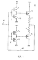
- a termination circuit according to an embodiment of the invention is shown in Fig. 1.
- inverter 1 consists of P-channel MOS transistor 11 and N-channel MOS transistor 12 which are connected in series between a power supply voltage V dd and ground potential
- inverter 2 also consists of P-channel MOS transistor 14 and N-channel MOS transistor 15 which are connected in series between the power supply voltage V dd and ground potential.
- the output of inverter 1 drives P-channel MOS transistor 13, and the output of inverter 2 drives N-channel MOS transistor 16.
- the output stage consists of a first transistor, P-channel MOS transistor 13, connected to the power supply voltage V dd , a second transistor, N-channel MOS transistor 16, connected to ground potential, and resistances 3 and 4 connected in series between P-channel MOS transistor 13 and N-channel MOS transistor 16.
- the output of the output stage is fed back via feedback line 17 from the junction of resistances 3 and 4, constituting an output node to the inputs of inverters 1 and 2.
- Input terminal 18 is connected to the far end of a transmission line.
- the sum of the impedance in the ON state of P-channel MOS transistor 13 and resistance 3 is selected so as to be substantially equal to the characteristic impedance thereof.
- the sum of the impedance in the ON state of N-channel MOS transistor 16 and resistance 4 is selected so as to be substantially equal to the characteristic impedance.
- the output stage in order to terminate the far end of the transmission line with the characteristic impedance of the transmission line, the output stage has resistances 3 and 4 in addition to the first and second transistors, and these resistances are used to make the termination impedance substantially equal to the characteristic impedance of the transmission line. Since such an output stage construction allows the impedances of P-channel MOS transistor 13 and N-channel MOS transistor 16 in the ON state to be selected to be small and since the termination impedance can be set mainly by resistances 3 and 4, high-performance termination that has excellent linearity for current and voltage is enabled. Furthermore, since the setting of the characteristic parameter of P-channel MOS transistor 13 and the value of resistance 3 and the setting of the characteristic parameter of N-channel MOS transistor 16 and the value of resistance 4 can be performed separately, the degree of freedom for circuit design becomes large.
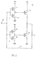
- the output stage may also be formed by providing resistance between the junction of the first 13 and second 16 transistor and the output node as shown in Fig. 2 instead of providing such a pair of resistances 3, 4 between the first 13 and second 16 transistors. Also in this case, the sum of the impedance of the first transistor 13 in the ON state and the resistance 5 is selected so as to be substantially equal to the characteristic impedance of the transmission line, and the sum of the impedance of the second transistor 16 in the ON state and the resistance 5 is selected so as to be substantially equal to the characteristic impedance of the transmission line.
- the circuit construction becomes simpler than in the previous case because only one resistance 5 is needed, although the degree of freedom of circuit design becomes smaller.
- the termination impedance can be set mainly with resistance, so that high-performance termination with excellent linearity for current and voltage is possible.
- Fig. 3 shows termination of a transmission line with the termination circuit shown in Fig. 1.
- Transmission line 24 has its input terminal 22 connected via resistance 25 to signal source 20, and its far-end terminal 23 connected to input terminal 18 of termination circuit 10.
- Resistance 25 is selected so as to be substantially equal the characteristic impedance of transmission line 24.
- Fig. 4 shows the input/output characteristics of the two inverters 1 and 2 constituting termination circuit 10, assuming that the maximum input voltage and power supply voltage V dd are 5V.
- Characteristic curve 31 represents the input/output characteristics of inverter 1
- characteristic curve 32 represents the input/output characteristics of inverter 2.
- Characteristic curve 32 shows that inverter 2 can positively turn off N-channel MOS transistor 16 when the input voltage changes from 0V to 2.5V, because the output voltage changes from 5V to 0.3V. Also, inverter 2 never turns on N-channel MOS transistor 16 when the input voltage changes from 5V to 2.5V, because the output voltage increases from 0V to only about 0.3V.
- N-channel MOS transistor 16 Since, in this case, the sum of resistance 4 and the ON-resistance of N-channel MOS transistor 16 is selected so as to be substantially equal to the characteristic impedance of transmission line 24, transmission line 24 is terminated with the characteristic impedance thereof. Because of this, the occurrence of a reflected wave due to noise at the far end of transmission line 24 is prevented. And, N-channel MOS transistor 16 connected to the ground potential is ON, one end of resistance 4 is equal to the ground potential, and the potential of terminal 23 of transmission line 24 is 0V and the other end of resistance 4 is also 0V, equal to the ground potential via feedback line 17, and thus no current flows through resistance 4, which results in zero power consumption in a steady state in which the signal voltage of transmission line 24 is 0V.
- Inverter 2 responds to potential change at terminal 23. That is, as is obvious from characteristic curve 32 of the input/output characteristics of inverter 2 shown in Fig. 4, the output voltage changes from 5V to substantially 0V as the input voltage changes from 0V to 2.5V. Since the output voltage of inverter 2 becomes substantially 0V, N-channel MOS transistor 16 is turned off. Since the current flowing through N-channel MOS transistor 16 to the ground potential is shut off when N-channel MOS transistor 16 is turned off, the current flowing in resistance 4 changes its direction and begins to propagate in the direction of terminal 22 of transmission line 24. This means that a reflected wave having a potential change from 0V to 2.5V occurs in terminal 23 of transmission line 24 as the current flowing in N-channel MOS transistor 16 is shut off.
- the potential of terminal 23 becomes 5V as a result of superposition of the reflected wave.
- the reflected wave is terminated by resistance 25, which is provided at the input of transmission line 24 and is equal to the characteristic impedance of transmission line 24, and is not reflected again at terminal 22 of transmission line 24.
- P-channel MOS transistor 13 connected to the 5V of the power supply voltage V dd , is ON and one end of resistance 3 is 5V, and in addition, the potential of terminal 23 of transmission line 24 is 5V and the other end of resistance 3 is also 5V via feedback line 17, and thus no current flows in resistance 3, which therefore results in zero power consumption at a steady state in which the signal voltage of transmission line 24 is 5V.
- N-channel MOS transistor 16 is turned off by the input/output characteristics of inverter 2 and the current flowing through N-channel MOS transistor 16 is shut off, so that a reflected wave causing a voltage increase of 2.5V occurs in terminal 23 of transmission line 24.
- the potential of terminal 23 of transmission line 24 is changed to 5V by the reflected wave to turn on P-channel MOS transistor 13, whereby terminal 23 of transmission line 24 is again terminated with the characteristic impedance thereof.
- the termination circuit 10 is constructed so that it allows the occurrence of a reflected wave only when a signal wave has reached the far end, thereby to double the voltage level of terminal 23 which is the far end of transmission line 24. That is, termination circuit 10 responds to a potential change in the signal wave on the order of +2.5V for allowing the occurrence of a reflected wave of about +2.5V.
- termination circuit 10 responds to a potential change in the signal wave on the order of +2.5V for allowing the occurrence of a reflected wave of about +2.5V.
- noise which is a potential change smaller than +2.5V, and is usually not greater than +1.5V, as is obvious from characteristic curves 31 and 32 of the input/output characteristics of inverters 1 and 2 shown in Fig.
- a reflected wave equal to a negative potential change having an amplitude of 2.5V occurs in terminal 23 of transmission line 24.
- the reflected wave propagates through transmission line 24 and is superposed on the potential change appearing at terminal 23, whereby the potential of terminal 23 of transmission line 24 is changed to zero.
- the reflected wave since the reflected wave propagates to terminal 22 of transmission line 24 and is terminated by resistance 25, which is equal to the characteristic impedance of transmission line 24, the reflected wave is not reflected again at terminal 22.
- N-channel MOS transistor 16 when the potential of terminal 23 of transmission line 24 becomes 0V, the output voltage of inverter 2 changes from nearly 0V to 5V, as seen from Fig. 3, and N-channel MOS transistor 16 in turn changes from OFF to ON.
- N-channel MOS transistor 16 becomes ON, since the sum of resistance 4 and the ON-resistance of N-channel MOS transistor 16 is preselected to be a value substantially equal to the characteristic impedance of transmission line 24, the far end of transmission line 24 is terminated with the characteristic impedance thereof. Accordingly, as detailed later, if noise (usually not greater than -1.5V) is induced in transmission line 24, the occurrence of a reflected wave due to the noise is prevented because of termination with the characteristic impedance thereof.
- N-channel MOS transistor 16 connected to the 0V of the ground potential, is ON and one end of resistance 4 is 0V, and the potential of terminal 23 of transmission line 24 is 0V and the other end of transmission 4 is also 0V via feedback line 17, no current flows in resistance 4, which therefore results in zero power consumption at a steady state in which the signal voltage on transmission line 24 is 0V.
- the termination circuit 10 is constructed so that it permits the occurrence of a reflected wave only when the signal wave has reached the far end to double the voltage level of terminal 23, which is the far end of transmission line 24. That is, termination circuit 10 responds to a potential change of about -2.5V in the signal wave to allow the occurrence of a reflected wave of the order of -2.5V.
- P-channel MOS transistor 13 and N-channel MOS transistor 16 in the output stage never be simultaneously ON for either a signal wave or noise, not only reduction of the noise but also substantial reduction of the power consumption can be accomplished.
- the termination circuit according to this invention has thoroughly solved the problem that the operation becomes unstable if reflection of a signal wave is suppressed at both input and far ends of a transmission line to perform an ideal signal transmission, as seen in the conventional termination circuit. If the termination circuit according to this invention is applied to a transmission line, the potential change at the input end of the transmission line propagates through the transmission line and appears at the far end, and a reflected wave substantially equal in phase therewith occurs in the far end and they are superposed on each other, so that it is accompanied with no waveform distortion.
- CMOS transistors a circuit using CMOS transistors
- this invention is not limited to a circuit using CMOS transistors, but the termination circuit according to this invention may be constructed using bipolar transistors.
- Fig. 5 For instance, one example of the termination circuit using bipolar transistors is shown in Fig. 5.
- the two CMOS inverters 1 and 2 are still used, but PNP bipolar transistor 42 and NPN bipolar transistors 46 are used in the output stage as alternates to P-channel MOS transistor 13 and N-channel MOS transistor 16, respectively.
- Resistances 43 and 44 are preselected so that the transmission line connected to input terminal 48 is terminated with the characteristic impedance thereof via feedback line 47.
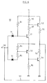
- FIG. 6 A further example of the termination circuit using bipolar transistors is shown in Fig. 6.
- the transistors used are all bipolar transistors. The operation of this termination circuit is now described. If the potential of input terminal 58 connected to the far end of a transmission line is assumed to be 0V as the initial condition, PNP bipolar transistor 52 and NPN bipolar transistor 54 are OFF and ON, respectively.
- NPN bipolar transistor 54 since the sum of resistance 56 and the ON-resistance of NPN bipolar transistor 54 is selected to a value substantially equal to the characteristic impedance of the transmission line, the transmission line is terminated with the characteristic impedance thereof. For this, the occurrence of a reflected wave due to a noise at the far end of the transmission line is prevented. And, since NPN bipolar transistor 54 is ON and one end of resistance 56 is at the ground potential, and the potential of input terminal 58 connected to the far end of the transmission line is 0V and by feedback line 57 the other end of resistance 56 is also 0V which is equal to the ground potential, no current flows in resistance 54, which therefore results in zero power consumption in a steady state in which the signal voltage of the transmission line is 0V.
- the sum of resistance 55 and the ON-resistance of PNP bipolar transistor 52 is preselected to a value substantially equal to the characteristic impedance of the transmission line, and accordingly the transmission line is terminated with the characteristic impedance thereof. This also prevents the occurrence of a reflected wave due to a noise at the far end of the transmission line.
- PNP bipolar transistor 52 connected to first potential V1 is ON and one end of resistance 55 is 5V, and the potential of input terminal 58 connected to the far end of the transmission line is 5V and the other end of resistance 55 is also 5V via feedback line 57, no current flows in resistance 55, which therefore results in zero power consumption at a steady state in which the signal voltage of the transmission line is 5V.
- first potential V1 is 5V and second potential V2 is 3V
- diode 71 is inserted so that no excessive current flows in the base of NPN bipolar transistor 51 when the potential of input terminal 58 is about 3V or higher
- resistance 81 is provided to supply a base current for turning on NPN bipolar transistor 51
- Resistance 83 is inserted so that no excessive current flows in the base of PNP bipolar transistor 52, and resistance 82 is provided to help PNP bipolar transistor 52 switch from ON to OFF.
- diode 72 is inserted to prevent a current flowing into second potential V2 at 3V via resistance 85 when the potential of input terminal 58 is about 2.5V or higher.
- Resistance 85 is inserted so that no excessive current flows in the base of PNP bipolar transistor 53, and resistance 84 is provided to help PNP bipolar transistor 53 switch from ON to OFF.
- resistance 86 is provided to help NPN bipolar transistor 54 switch from ON to OFF.
- the current when NPN bipolar transistor 51 and PNP bipolar transistor 53 are in an ON state may be selected to a small value, which therefore makes it possible to reduce the power required in the terminal circuit.
Landscapes
- Engineering & Computer Science (AREA)
- Power Engineering (AREA)
- Computer Networks & Wireless Communication (AREA)
- Signal Processing (AREA)
- Robotics (AREA)
- Mechanical Engineering (AREA)
- Logic Circuits (AREA)
- Cable Transmission Systems, Equalization Of Radio And Reduction Of Echo (AREA)
Applications Claiming Priority (2)
| Application Number | Priority Date | Filing Date | Title |
|---|---|---|---|
| JP16246/92 | 1992-01-31 | ||
| JP4016246A JPH073958B2 (ja) | 1992-01-31 | 1992-01-31 | 終端回路 |
Publications (2)
| Publication Number | Publication Date |
|---|---|
| EP0554121A2 true EP0554121A2 (fr) | 1993-08-04 |
| EP0554121A3 EP0554121A3 (en) | 1994-07-27 |
Family
ID=11911201
Family Applications (1)
| Application Number | Title | Priority Date | Filing Date |
|---|---|---|---|
| EP19930300691 Withdrawn EP0554121A3 (en) | 1992-01-31 | 1993-01-29 | Line termination circuit |
Country Status (3)
| Country | Link |
|---|---|
| US (1) | US5329190A (fr) |
| EP (1) | EP0554121A3 (fr) |
| JP (1) | JPH073958B2 (fr) |
Cited By (4)
| Publication number | Priority date | Publication date | Assignee | Title |
|---|---|---|---|---|
| WO1995024089A3 (fr) * | 1994-02-25 | 1995-10-05 | Ericsson Telefon Ab L M | Reseau de terminaison et circuit de commande |
| GB2408640A (en) * | 2003-11-28 | 2005-06-01 | Hewlett Packard Development Co | A termination circuit with partial current shunting |
| US7161379B2 (en) | 2004-04-14 | 2007-01-09 | Hewlett-Packard Development Company, L.P. | Shunted current reduction |
| USRE41598E1 (en) | 2001-03-13 | 2010-08-31 | Realtek Semiconductor Corp. | Impedance matching circuit |
Families Citing this family (26)
| Publication number | Priority date | Publication date | Assignee | Title |
|---|---|---|---|---|
| DE3048067C2 (de) * | 1980-12-19 | 1984-08-09 | Kuka Schweissanlagen + Roboter Gmbh, 8900 Augsburg | Getriebeanordnung für den Gelenkkopf eines Manipulators |
| US5634014A (en) * | 1993-06-18 | 1997-05-27 | Digital Equipment Corporation | Semiconductor process, power supply voltage and temperature compensated integrated system bus termination |
| FR2709217B1 (fr) * | 1993-08-19 | 1995-09-15 | Bull Sa | Procédé et dispositif d'adaptation d'impédance pour un émetteur et/ou récepteur, circuit intégré et système de transmission les mettant en Óoeuvre. |
| JP3400853B2 (ja) * | 1994-04-27 | 2003-04-28 | 三菱電機株式会社 | 半導体装置 |
| US5491436A (en) * | 1994-07-29 | 1996-02-13 | International Business Machines Corp. | Compensated CMOS driver circuit with reduced DC losses |
| EP0746128B1 (fr) * | 1995-05-30 | 2002-09-25 | STMicroelectronics S.r.l. | Circuit d'interface de ligne téléphonique avec impédance de terminaison pendant les pauses du signal d'appel |
| JP3192937B2 (ja) * | 1995-08-31 | 2001-07-30 | 株式会社東芝 | バスホールド回路 |
| US5726583A (en) * | 1996-07-19 | 1998-03-10 | Kaplinsky; Cecil H. | Programmable dynamic line-termination circuit |
| US5760601A (en) * | 1996-08-26 | 1998-06-02 | International Business Machines Corporation | Transmission line driver circuit for matching transmission line characteristic impedance |
| US5815107A (en) * | 1996-12-19 | 1998-09-29 | International Business Machines Corporation | Current source referenced high speed analog to digitial converter |
| US5923276A (en) * | 1996-12-19 | 1999-07-13 | International Business Machines Corporation | Current source based multilevel bus driver and converter |
| US6275088B1 (en) * | 1997-09-30 | 2001-08-14 | Intel Corporation | Method and apparatus for dynamic impedance clamping of a digital signal delivered over a transmission line |
| US6054881A (en) * | 1998-01-09 | 2000-04-25 | Advanced Micro Devices, Inc. | Input/output (I/O) buffer selectively providing resistive termination for a transmission line coupled thereto |
| US6127840A (en) * | 1998-03-17 | 2000-10-03 | International Business Machines Corporation | Dynamic line termination clamping circuit |
| US20030017138A1 (en) * | 1998-07-08 | 2003-01-23 | Menzo Havenga | Chimeric adenoviruses |
| US6316969B1 (en) * | 1999-02-26 | 2001-11-13 | Micron Technology, Inc. | Differential receivers in a CMOS process |
| JP4119062B2 (ja) * | 1999-10-25 | 2008-07-16 | 日本テキサス・インスツルメンツ株式会社 | 終端回路 |
| US6320427B1 (en) * | 2000-10-11 | 2001-11-20 | Winbond Electronics Corp. | High-speed, low-power continuous-time CMOS current comparator |
| US6351138B1 (en) * | 2001-03-22 | 2002-02-26 | Pericom Semiconductor Corp. | Zero-DC-power active termination with CMOS overshoot and undershoot clamps |
| US6541998B2 (en) * | 2001-04-17 | 2003-04-01 | Cypress Semiconductor Corp. | Active termination circuit with an enable/disable |
| US7102200B2 (en) * | 2001-09-04 | 2006-09-05 | Intel Corporation | On-die termination resistor with analog compensation |
| US6686763B1 (en) | 2002-05-16 | 2004-02-03 | Pericam Semiconductor Corp. | Near-zero propagation-delay active-terminator using transmission gate |
| KR100486301B1 (ko) * | 2003-01-27 | 2005-04-29 | 삼성전자주식회사 | 전력 소비를 감소시키는 종단 회로. |
| US8064175B2 (en) * | 2005-09-15 | 2011-11-22 | Rambus Inc. | Power supply shunt |
| KR100881195B1 (ko) * | 2007-05-22 | 2009-02-05 | 삼성전자주식회사 | 고주파 성능을 개선한 odt 회로 |
| JP2023102112A (ja) | 2022-01-11 | 2023-07-24 | ソニーセミコンダクタソリューションズ株式会社 | 終端回路および半導体回路 |
Family Cites Families (2)
| Publication number | Priority date | Publication date | Assignee | Title |
|---|---|---|---|---|
| US4112262A (en) * | 1977-07-26 | 1978-09-05 | Bell Telephone Laboratories, Incorporated | Telephone station repeater |
| JPH02196528A (ja) * | 1989-01-26 | 1990-08-03 | Fujitsu Ltd | 終端回路 |
-
1992
- 1992-01-31 JP JP4016246A patent/JPH073958B2/ja not_active Expired - Lifetime
- 1992-07-20 US US07/916,920 patent/US5329190A/en not_active Expired - Fee Related
-
1993
- 1993-01-29 EP EP19930300691 patent/EP0554121A3/en not_active Withdrawn
Cited By (8)
| Publication number | Priority date | Publication date | Assignee | Title |
|---|---|---|---|---|
| WO1995024089A3 (fr) * | 1994-02-25 | 1995-10-05 | Ericsson Telefon Ab L M | Reseau de terminaison et circuit de commande |
| AU686763B2 (en) * | 1994-02-25 | 1998-02-12 | Telefonaktiebolaget Lm Ericsson (Publ) | A termination network and a control circuit |
| CN1083195C (zh) * | 1994-02-25 | 2002-04-17 | 艾利森电话股份有限公司 | 一种端接网络与控制电路 |
| USRE41598E1 (en) | 2001-03-13 | 2010-08-31 | Realtek Semiconductor Corp. | Impedance matching circuit |
| GB2408640A (en) * | 2003-11-28 | 2005-06-01 | Hewlett Packard Development Co | A termination circuit with partial current shunting |
| US6970011B2 (en) | 2003-11-28 | 2005-11-29 | Hewlett-Packard Development Company, L.P. | Partial termination voltage current shunting |
| US7088130B2 (en) | 2003-11-28 | 2006-08-08 | Hewlett-Packard Development Company, L.P. | Partial termination voltage current shunting |
| US7161379B2 (en) | 2004-04-14 | 2007-01-09 | Hewlett-Packard Development Company, L.P. | Shunted current reduction |
Also Published As
| Publication number | Publication date |
|---|---|
| US5329190A (en) | 1994-07-12 |
| EP0554121A3 (en) | 1994-07-27 |
| JPH05276070A (ja) | 1993-10-22 |
| JPH073958B2 (ja) | 1995-01-18 |
Similar Documents
| Publication | Publication Date | Title |
|---|---|---|
| EP0554121A2 (fr) | Circuit de terminaison de ligne | |
| US4877978A (en) | Output buffer tri-state noise reduction circuit | |
| USRE34808E (en) | TTL/CMOS compatible input buffer with Schmitt trigger | |
| JP2549743B2 (ja) | 出力回路 | |
| JPS61136316A (ja) | レベル移動回路 | |
| US6285209B1 (en) | Interface circuit and input buffer integrated circuit including the same | |
| US20030038655A1 (en) | Differential amplifier and semiconductor integrated circuit for LCD drive | |
| US20030098712A1 (en) | Level conversion circuit for which an operation at power voltage rise time is stabilized | |
| US4393315A (en) | High-gain stabilized converter | |
| EP0110317B1 (fr) | Circuit pilote de faible consommation pour lignes numériques à grand débit | |
| JP2611022B2 (ja) | 増幅器 | |
| JPH02222216A (ja) | BiCMOSドライバ回路 | |
| US4808944A (en) | High accuracy differential output stage | |
| JP3492765B2 (ja) | レベル変換回路 | |
| US6046617A (en) | CMOS level detection circuit with hysteresis having disable/enable function and method | |
| US4998028A (en) | High speed CMOS logic device for providing ECL compatible logic levels | |
| KR19990087228A (ko) | 내부전압 기준출력 구동기 | |
| US5311075A (en) | Level shifting CMOS integrated circuits | |
| JP3159247B2 (ja) | 入力回路 | |
| US5338980A (en) | Circuit for providing a high-speed logic transition | |
| US5847576A (en) | Low power, variable logic threshold voltage, logic gates | |
| US6563342B1 (en) | CMOS ECL output buffer | |
| KR100239717B1 (ko) | 데이타 출력버퍼 | |
| KR100457343B1 (ko) | 저소비 전류의 더블 버퍼 회로 | |
| JP2745619B2 (ja) | 出力回路 |
Legal Events
| Date | Code | Title | Description |
|---|---|---|---|
| PUAI | Public reference made under article 153(3) epc to a published international application that has entered the european phase |
Free format text: ORIGINAL CODE: 0009012 |
|
| AK | Designated contracting states |
Kind code of ref document: A2 Designated state(s): DE FR GB |
|
| 17P | Request for examination filed |
Effective date: 19931119 |
|
| PUAL | Search report despatched |
Free format text: ORIGINAL CODE: 0009013 |
|
| AK | Designated contracting states |
Kind code of ref document: A3 Designated state(s): DE FR GB |
|
| 18W | Application withdrawn |
Withdrawal date: 19951129 |