EP0554593B1 - Procédé de fabrication d'un dispositif qui utilise un substrat d'un matériau présentant l'effet pyroélectrique - Google Patents
Procédé de fabrication d'un dispositif qui utilise un substrat d'un matériau présentant l'effet pyroélectrique Download PDFInfo
- Publication number
- EP0554593B1 EP0554593B1 EP92300947A EP92300947A EP0554593B1 EP 0554593 B1 EP0554593 B1 EP 0554593B1 EP 92300947 A EP92300947 A EP 92300947A EP 92300947 A EP92300947 A EP 92300947A EP 0554593 B1 EP0554593 B1 EP 0554593B1
- Authority
- EP
- European Patent Office
- Prior art keywords
- substrate
- film
- top surface
- electrode
- region
- Prior art date
- Legal status (The legal status is an assumption and is not a legal conclusion. Google has not performed a legal analysis and makes no representation as to the accuracy of the status listed.)
- Expired - Lifetime
Links
Images
Classifications
-
- G—PHYSICS
- G02—OPTICS
- G02F—OPTICAL DEVICES OR ARRANGEMENTS FOR THE CONTROL OF LIGHT BY MODIFICATION OF THE OPTICAL PROPERTIES OF THE MEDIA OF THE ELEMENTS INVOLVED THEREIN; NON-LINEAR OPTICS; FREQUENCY-CHANGING OF LIGHT; OPTICAL LOGIC ELEMENTS; OPTICAL ANALOGUE/DIGITAL CONVERTERS
- G02F1/00—Devices or arrangements for the control of the intensity, colour, phase, polarisation or direction of light arriving from an independent light source, e.g. switching, gating or modulating; Non-linear optics
- G02F1/01—Devices or arrangements for the control of the intensity, colour, phase, polarisation or direction of light arriving from an independent light source, e.g. switching, gating or modulating; Non-linear optics for the control of the intensity, phase, polarisation or colour
- G02F1/03—Devices or arrangements for the control of the intensity, colour, phase, polarisation or direction of light arriving from an independent light source, e.g. switching, gating or modulating; Non-linear optics for the control of the intensity, phase, polarisation or colour based on ceramics or electro-optical crystals, e.g. exhibiting Pockels effect or Kerr effect
- G02F1/035—Devices or arrangements for the control of the intensity, colour, phase, polarisation or direction of light arriving from an independent light source, e.g. switching, gating or modulating; Non-linear optics for the control of the intensity, phase, polarisation or colour based on ceramics or electro-optical crystals, e.g. exhibiting Pockels effect or Kerr effect in an optical waveguide structure
-
- G—PHYSICS
- G02—OPTICS
- G02F—OPTICAL DEVICES OR ARRANGEMENTS FOR THE CONTROL OF LIGHT BY MODIFICATION OF THE OPTICAL PROPERTIES OF THE MEDIA OF THE ELEMENTS INVOLVED THEREIN; NON-LINEAR OPTICS; FREQUENCY-CHANGING OF LIGHT; OPTICAL LOGIC ELEMENTS; OPTICAL ANALOGUE/DIGITAL CONVERTERS
- G02F1/00—Devices or arrangements for the control of the intensity, colour, phase, polarisation or direction of light arriving from an independent light source, e.g. switching, gating or modulating; Non-linear optics
- G02F1/01—Devices or arrangements for the control of the intensity, colour, phase, polarisation or direction of light arriving from an independent light source, e.g. switching, gating or modulating; Non-linear optics for the control of the intensity, phase, polarisation or colour
- G02F1/21—Devices or arrangements for the control of the intensity, colour, phase, polarisation or direction of light arriving from an independent light source, e.g. switching, gating or modulating; Non-linear optics for the control of the intensity, phase, polarisation or colour by interference
- G02F1/225—Devices or arrangements for the control of the intensity, colour, phase, polarisation or direction of light arriving from an independent light source, e.g. switching, gating or modulating; Non-linear optics for the control of the intensity, phase, polarisation or colour by interference in an optical waveguide structure
-
- G—PHYSICS
- G02—OPTICS
- G02F—OPTICAL DEVICES OR ARRANGEMENTS FOR THE CONTROL OF LIGHT BY MODIFICATION OF THE OPTICAL PROPERTIES OF THE MEDIA OF THE ELEMENTS INVOLVED THEREIN; NON-LINEAR OPTICS; FREQUENCY-CHANGING OF LIGHT; OPTICAL LOGIC ELEMENTS; OPTICAL ANALOGUE/DIGITAL CONVERTERS
- G02F1/00—Devices or arrangements for the control of the intensity, colour, phase, polarisation or direction of light arriving from an independent light source, e.g. switching, gating or modulating; Non-linear optics
- G02F1/29—Devices or arrangements for the control of the intensity, colour, phase, polarisation or direction of light arriving from an independent light source, e.g. switching, gating or modulating; Non-linear optics for the control of the position or the direction of light beams, i.e. deflection
- G02F1/31—Digital deflection, i.e. optical switching
- G02F1/313—Digital deflection, i.e. optical switching in an optical waveguide structure
- G02F1/3132—Digital deflection, i.e. optical switching in an optical waveguide structure of directional coupler type
-
- G—PHYSICS
- G02—OPTICS
- G02F—OPTICAL DEVICES OR ARRANGEMENTS FOR THE CONTROL OF LIGHT BY MODIFICATION OF THE OPTICAL PROPERTIES OF THE MEDIA OF THE ELEMENTS INVOLVED THEREIN; NON-LINEAR OPTICS; FREQUENCY-CHANGING OF LIGHT; OPTICAL LOGIC ELEMENTS; OPTICAL ANALOGUE/DIGITAL CONVERTERS
- G02F2201/00—Constructional arrangements not provided for in groups G02F1/00 - G02F7/00
- G02F2201/06—Constructional arrangements not provided for in groups G02F1/00 - G02F7/00 integrated waveguide
- G02F2201/066—Constructional arrangements not provided for in groups G02F1/00 - G02F7/00 integrated waveguide channel; buried
-
- G—PHYSICS
- G02—OPTICS
- G02F—OPTICAL DEVICES OR ARRANGEMENTS FOR THE CONTROL OF LIGHT BY MODIFICATION OF THE OPTICAL PROPERTIES OF THE MEDIA OF THE ELEMENTS INVOLVED THEREIN; NON-LINEAR OPTICS; FREQUENCY-CHANGING OF LIGHT; OPTICAL LOGIC ELEMENTS; OPTICAL ANALOGUE/DIGITAL CONVERTERS
- G02F2201/00—Constructional arrangements not provided for in groups G02F1/00 - G02F7/00
- G02F2201/07—Constructional arrangements not provided for in groups G02F1/00 - G02F7/00 buffer layer
-
- G—PHYSICS
- G02—OPTICS
- G02F—OPTICAL DEVICES OR ARRANGEMENTS FOR THE CONTROL OF LIGHT BY MODIFICATION OF THE OPTICAL PROPERTIES OF THE MEDIA OF THE ELEMENTS INVOLVED THEREIN; NON-LINEAR OPTICS; FREQUENCY-CHANGING OF LIGHT; OPTICAL LOGIC ELEMENTS; OPTICAL ANALOGUE/DIGITAL CONVERTERS
- G02F2202/00—Materials and properties
- G02F2202/20—LiNbO3, LiTaO3
-
- G—PHYSICS
- G02—OPTICS
- G02F—OPTICAL DEVICES OR ARRANGEMENTS FOR THE CONTROL OF LIGHT BY MODIFICATION OF THE OPTICAL PROPERTIES OF THE MEDIA OF THE ELEMENTS INVOLVED THEREIN; NON-LINEAR OPTICS; FREQUENCY-CHANGING OF LIGHT; OPTICAL LOGIC ELEMENTS; OPTICAL ANALOGUE/DIGITAL CONVERTERS
- G02F2203/00—Function characteristic
- G02F2203/21—Thermal instability, i.e. DC drift, of an optical modulator; Arrangements or methods for the reduction thereof
Definitions
- This invention relates to a method of manufacturing a device employing a substrate of a material that exhibits the pyroelectric effect.
- LiNbO 3 lithium niobate
- optical waveguides are formed in a monocrystalline substrate of LiNbO 3 by diffusion of titanium into the crystal structure, and electrodes are deposited over a front surface of the substrate.
- a buffer layer of SiO 2 may be interposed between the substrate and the electrodes.
- a buffer layer may be deposited on the back surface of the substrate. A potential difference is established between the electrodes, and the electric field that is thereby created in the LiNbO 3 substrate influences the coupling of optical energy between the two waveguides.
- An optical switch may be used in an optical time domain reflectometer (OTDR) to direct light emitted from a light source into a fiber under test and direct reflected and back-scattered light from the fiber under test to a detector, depending on the field existing in the substrate. It is desirable that the field that affects the condition of the switch depend only on the potential difference between the electrodes.
- OTDR optical time domain reflectometer
- LiNbO 3 exhibits the pyroelectric effect.
- the pyroelectric effect causes a change in the spontaneous polarization of the material, and this produces a proportional electric field in the material along its Z-axis. Therefore, when the temperature of an optical switch based on LiNbO 3 changes, the behavior of optical modes propagating through the waveguides is influenced not only by the potential difference established between the electrodes but also by the pyroelectric field.
- the pyroelectric effect is self-extinguishing, since the pyroelectric field will result in charge being attracted to the Z faces of the substrate, and this charge will produce an electric field opposite in direction to the pyroelectric field. Given sufficient time (on the order of an hour in typical room air), an equilibrium state will be reached in which the accumulated surface charge produces a field that exactly cancels the pyroelectric field.
- An integrated optic device such as an optical switch, generally has conductive electrodes over some parts of its surface but not others. This inevitably causes the equilibrating process to proceed at a faster pace in the material directly underneath electrodes than in adjacent areas.
- the electric field in the crystal will be different in the two regions.
- a plot of the field would show complicated fringing shapes at electrode edges. Waveguides located in various positions with respect to electrode edges will be subjected to various field strengths, so waveguide coupling will be disturbed as though a complex external field had been applied.
- the equilibrating process can be made essentially instantaneous if the Z faces of the crystal are covered by conductive films and the films are electrically connected during the temperature change, since the conductive films contain mobile charge carriers that will respond immediately to the pyroelectric field by redistributing between the surfaces so as to cancel the pyroelectric field.
- an electrooptic device which may be considered to comprise: a substrate of an electrooptic material, in this case LiNbO 3 , that exhibits the pyroelectric effect, the substrate having a top surface and there being a waveguide, preferably a titanium-diffused waveguide, in the substrate beneath said top surface, an insulating buffer layer of SiO 2 , overlying the top surface of the substrate, the buffer layer having a bottom surface that confronts the top surface of the substrate and also having a top surface, and an electrode over the said buffer layer and positioned so that a line that is normal to the top surface of the substrate and passes through the waveguide also passes through the electrode.
- an electrooptic device which may be considered to comprise: a substrate of an electrooptic material, in this case LiNbO 3 , that exhibits the pyroelectric effect, the substrate having a top surface and there being a waveguide, preferably a titanium-diffused waveguide, in the substrate beneath said top surface, an insulating buffer layer of SiO 2 , over
- a semi-insulating film of indium tin oxide (ITO) be provided over the front surface of the electrooptic device, covering the electrodes and the exposed surface of the substrate.
- the ITO film reduces the resistance between the electrodes of the device by at least three orders of magnitude and results in a more uniform distribution of pyroelectric surface charge over the device.
- a disadvantage of the structure disclosed by Sawaki et al arises from the difficulty of ensuring a continuous film of ITO over the front surface of the device, since the electrodes cause step coverage problems and the small spacing between the electrodes makes it difficult to deposit material between the electrodes.
- a method of manufacturing an electrooptic device comprising the steps of: (a) providing a substrate of an electrooptic material, preferably LiNbO 3 , that exhibits the pyroelectric effect, the substrate having a waveguide, preferably a titanium-diffused waveguide, formed therein beneath a top surface thereof, (b) forming an insulating buffer layer, preferably of SiO 2 , over the top surface of the substrate, the buffer layer having a bottom surface that confronts the top surface of the substrate and also having a top surface, and (c) forming an electrode over the buffer layer, said electrode being positioned so that a line that is normal to the top surface of the substrate and passes through the waveguide also passes through the electrode, characterised by depositing, between steps (b) and (c), a film containing a selected material, preferably a refractory metal and most preferably titanium, in a low resistivity state over the top surface of the buffer layer, said electrode being formed on a
- an electrooptic device comprising a substrate of an electrooptic material, preferably LiNbO 3 , that exhibits the pyroelectric effect, the substrate having a top surface and there being a waveguide, preferably a titanium-diffused waveguide, in the substrate beneath said top surface, an insulating buffer layer, preferably of SiO 2 , overlying the top surface of the substrate, the buffer layer having a bottom surface that confronts the top surface of the substrate and also having a top surface, and an electrode over the said buffer layer and positioned so that a line that is normal to the top surface of the substrate and passes through the waveguide also passes through the electrode; characterised by a film over the top surface of the buffer layer, said film including a selected material, preferably a refractory metal and most preferably titanium, and having a high resistivity region and a low resistivity region, said electrode overlying the low resistivity region of said film while leaving the high resistivity region exposed.
- an electrooptic material preferably LiNbO 3
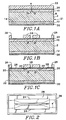
- FIG. 1A illustrates a substrate 2 of z-cut monocrystalline LiNbO 3 .
- Substrate 2 is one of several identical substrates that are formed from a monocrystalline wafer of z-cut LiNbO 3 .
- two diffused titanium waveguides 4 are formed in substrate 2 beneath its front surface 8.
- Formation of diffused Ti waveguides in LiNbO 3 typically involves treatment at temperatures on the order of 1000° C.
- a buffer layer 10 of SiO 2 is formed over front surface 8 by chemical vapor deposition.
- a buffer layer 12 is formed over the back surface 14 of substrate 2.
- layer 12 is not necessary to the operation of the illustrated device.
- a thin film 20 of Ti is deposited over the front surface of the die 21 composed of substrate 2 and buffer layers 10, 12, and a continuous layer 22 of Al is deposited over film 20.
- a continuous layer 30 of Al is deposited over buffer layer 12.
- layer 22 is patterned using standard photolithographic techniques to define two discrete electrodes 24 and a ring 26 that extends around the periphery of film 20. In the state shown in FIG. 1B, film 20 is highly conductive, so that the electrical resistance between electrodes 24 is negligible.
- the structure shown in FIG. 1B is baked in an atmosphere of oxygen and nitrogen. During the baking operation, in which temperatures in excess of about 250°C are attained, exposed portions 28 of metallic film 20 are converted to a high resistivity state. After the baking operation, the wafer is diced, and a stripe 32 of conductive paint is applied to the side of die 21 to connect ring 26 to layer 30. The completed optical switch is shown in FIG. 2.
- stripe 32 When a temperature change causes a pyroelectric field to be generated between the faces of substrate 2, stripe 32 allows charge to be redistributed between films 20 and 30 to produce a counteracting field so that there is is no net field in the substrate. This occurs within a time on the order of milliseconds. Therefore, the time required to achieve equilibrium between the pyroelectric field and the field due to surface charge is very short, and for most purposes no instability in performance of the switch due to change in temperature is observed.
- the high resistivity of portions 28 of film 20 prevents excessive power dissipation when voltage is applied between electrodes 22.
- the baking operation is composed of at least one baking cycle, which comprises a heat-up phase, a constant temperature phase and a cool-down phase.
- the maximum temperature that is attained during the baking operation may be in the range from about 350°C to about 400°C, which is sufficiently low that the properties of the diffused waveguides are not affected significantly.
- the heat-up phase lasts about 15 minutes and the constant temperature phase of the first baking cycle lasts about 30 minutes. Cooling to 250°C is controlled to take place quite slowly, e.g. over a period of 70 minutes, because conversion of the metallic film to its high resistivity state continues at a significant rate until the temperature falls below about 250°C.
- the cooling may be accelerated after the initial portion of the cool-down phase.
- the resistivity of exposed portions 28 is measured. If the resistivity is in the desired range, which may be, for example, lE7 to lE11 ohms per square, the baking operation is discontinued. Otherwise, a second baking cycle is performed, and the length of the constant temperature phase of the second cycle depends on how close the measured value of the resistivity is to the desired range of values.
- the baking operation does not affect the portions of layer 20 that lie beneath electrodes 24 and ring 26.
- the nature of the change in the exposed portions of film 20 that takes place during the baking operation is not fully understood.
- the composition of exposed portions 28 of converted film 20 was measured by electron scanning chemical analysis, in which material is progressively removed by sputtering and the composition of the exposed material is measured by auger analysis. It was found that for small depths, portions 28 contain titanium and oxygen in an approximately stoichiometric ratio, which suggests that portions 28 are titanium dioxide. For greater depths, Si, Ti and O 2 were found, indicating diffusion between buffer layer 10 and film 20, and they were present in the stoichiometric ratios of SiO 2 and TiO 2 . These analysis results imply that exposed portions 28 would be electrically insulating. However, measurement of the resistance between electrodes 24 indicates that although the resistivity of portions 28 is much higher than the resistivity of metallic Ti, the material of portions 28 still exhibits a finite conductivity.
- the invention is not restricted to the particular embodiment that has been described, and that variations may be made therein without departing from the scope of the invention as defined in the appended claims and equivalents thereof.
- the invention is not restricted to application to an optical switch, but may also be applied to other electrooptic devices such as interferometers and modulators.
- the invention is not limited to use of titanium as the material of film 20, since other materials may be used in a similar process to achieve a similar result.
- the invention is not restricted to the particular process steps that have been described.
- layer 30 may be deposited after the wafer is diced, in which case layers of Al may be deposited simultaneously on the sides of the die so that the separate step of depositing paint stripe 32 is not required.
- Layer 30 need not be adhered directly to die, and its function may be provided by mounting die 21 on a metal plate. Treatments other than heating in an atmosphere containing oxygen may be used to modify the material of the film deposited on the front surface of the die to convert it to the state in which it has the desired resistivity. It is intended that the claims should not be interpreted as being limited to the treatment being performed in cycles, but to cover also methods in which the resistivity is measured throughout the treatment and the treatment is discontinued when the resistivity reaches the desired level.
- an embodiment of the present invention can provide a method of manufacturing an electrooptic device comprising providing a substrate of a material that exhibits the pyroelectric effect, depositing a film containing a selected material in a first state over a front surface of the substrate, and subjecting portions of the film to a predetermined treatment such that they are converted from the first state to a second state in which the material has a resistivity that lies within a desired range of values.
- Another embodiment of the present invention can provide an electrooptic device comprising a substrate of a material that exhibits the pyroelectric effect and has a front surface, a film containing a selected material over the front surface of the substrate, the selected material having a first state, in which its resistivity lies within a desired range of values, and a second state, in which its resistivity lies outside that range of values, and at least one electrode overlying the film while leaving portions of the film exposed, the portions of the film that lie beneath the electrode beneath the electrode being in the second state and the portions that are exposed being in the first state.
Landscapes
- Physics & Mathematics (AREA)
- Nonlinear Science (AREA)
- Chemical & Material Sciences (AREA)
- Engineering & Computer Science (AREA)
- Ceramic Engineering (AREA)
- Crystallography & Structural Chemistry (AREA)
- General Physics & Mathematics (AREA)
- Optics & Photonics (AREA)
- Optical Integrated Circuits (AREA)
Claims (10)
- Procédé de fabrication d'un dispositif électro-optique, comprenant les étapes consistant à :(a) procurer un substrat (2) d'un matériau électro-optique, de préférence du LiNbO3, qui présente l'effet pyroélectrique, le substrat comportant un guide d'onde (4), de préférence un guide d'onde à titane diffusé, formé dans celui-ci au-dessous d'une surface supérieure (8) de celui-ci,(b) former une couche tampon isolante (10), de préférence de SiO2, sur la surface supérieure du substrat, la couche tampon comportant une surface inférieure qui est face à la surface supérieure du substrat et comportant également une surface supérieure, et(c) former une électrode (24) sur la couche tampon, ladite électrode étant positionnée de façon à ce qu'une ligne qui est normale à la surface supérieure du substrat et qui passe par le guide d'onde, passe également au travers de l'électrode,caractérisé par un dépôt, entre les étapes (b) et (c), d'un film (20) contenant un matériau sélectionné, de préférence un métal réfractaire et de la façon la plus préférée, du titane, dans un état de faible résistivité sur la surface supérieure de la couche tampon (10), ladite électrode étant formée sur une première région dudit film tout en laissant exposée une seconde région (28) dudit film, et ledit matériau pouvant être converti de son état de faible résistivité en un état de forte résistivité lorsqu'il est soumis à un traitement prédéterminé, de préférence en le chauffant en présence d'oxygène, et
caractérisé en outre par une étape (d), après l'étape (c), consistant à exposer ladite seconde région dudit film à un agent prédéterminé, de préférence de l'oxygène, dans des conditions telles que ladite seconde région du film est soumise audit traitement prédéterminé, ladite première région du film étant masquée par rapport à l'agent prédéterminé par l'électrode, et n'étant de ce fait pas soumise audit traitement prédéterminé. - Procédé selon la revendication 1, dans lequel le substrat (2) qui est procuré à l'étape (a) comporte des premier et second guides d'onde (4) formés dans celui-ci, ladite première région du film comporte des première et seconde parties, et l'étape (c) comprend la formation de première et seconde électrodes (24) sur lesdites première et seconde parties, respectivement, de ladite première région du film, les électrodes étant positionnées de façon à ce qu'une ligne qui est normale à la surface supérieure du substrat et passe par le premier guide d'onde, passe également au travers de la première électrode et qu'une ligne qui est normale à la surface supérieure du substrat et passe par le second guide d'onde, passe également au travers de la seconde électrode, une partie de la seconde région dudit film étant exposée entre lesdites électrodes.
- Procédé selon la revendication 1 ou 2, dans lequel l'étape (c) comprend le dépôt d'une couche (22) de métal sur ledit film (20) et l'élimination sélective de ladite couche pour former ladite électrode (24) ou chaque dite électrode et une partie de borne (26).
- Procédé selon la revendication 3, comprenant en outre le dépôt d'unc couche (30) de matériau conducteur sur une surface inférieure du substrat (2) et la connexion de ladite partie de borne à ladite couche de matériau conducteur.
- Procédé selon la revendication 1, comprenant en outre le dépôt d'une couche (30) de matériau conducteur sur une surface inférieurc du substrat (2) et la connexion électrique de ladite couche audit film (20).
- Procédé selon la revendication 2, comprenant en outre la mesure dc la résistance électrique entre les première et seconde électrodes (24).
- Dispositif électro-optique comprenant :un substrat (2) d'un matériau électro-optique, de préférence du LiNbO3, qui présente l'effet pyroélectrique, le substrat comportant une surface supérieure (8) incluant un guide d'onde (4), de préférence un guide d'onde au titane diffusé, dans le substrat au-dessous de ladite surface supérieure,une couche tampon isolante (10), de préférence de SiO2, recouvrant la surface supérieure du substrat, la couche tampon comportant une surface inférieure qui est face à la surface supérieure du substrat et comportant également une surface supérieure, etune électrode (24) sur ladite couche tampon et positionnée de façon à ce qu'une ligne qui est normale à la surface supérieure du substrat et passe par le guide d'onde, passe également au travers de l'électrode,caractérisé par :
un film (20) sur la surface supérieure de la couche tampon, ledit film comprenant un matériau sélectionné, de préférence un métal réfractaire et de la façon la plus préférée du titane, et présentant une région à forte résistivité (28) et une région à faible résistivité, ladite électrode (24) recouvrant la région à faible résistivité dudit film tout en laissant exposée la région à forte résistivité (28). - Dispositif électro-optique selon la revendication 7, dans lequel le substrat (2) comporte des premier et second guides d'onde (4) formés dans celui-ci au-dessous de la surface supérieure (8) de celui-ci, la région à faible résistivité du film comporte des première et seconde parties, et le dispositif comprend des première et seconde électrodes discrètes (24) recouvrant respectivement lesdites première et seconde parties de ladite région à faible résistivité du film tout en laissant exposée une partie de la région à forte résistivité (28) entre celles-ci, lesdites électrodes étant positionnées de façon à ce qu'une ligne qui est normale à la surface supérieure du substrat et passe par le premier guide d'onde, passe également au travers de la première électrode et qu'une ligne qui est normale à la surface supérieure du substrat et passe par le second guide d'onde, passe également au travers de la seconde électrode.
- Dispositif électro-optique selon la revendication 7 ou 8, dans lequel le substrat (2) comporte une surface inférieure et le dispositif comprend une couche de métal (3) sur la surface inférieure du substrat, la couche de métal étant reliée électriquement au film (20).
- Dispositif électro-optique selon la revendication 9, dans lequcl la région à faible résistivité du film (20) comporte une partie de borne. ct le dispositif comprend une partie de borne (26) de métal recouvrant la partie de borne dudit film, et un matériau conducteur (32) reliant ladite partie de borne à la couche de métal (30).
Priority Applications (1)
| Application Number | Priority Date | Filing Date | Title |
|---|---|---|---|
| DE1992622841 DE69222841T2 (de) | 1992-02-04 | 1992-02-04 | Verfahren zur Herstellung einer Vorrichtung, die ein Substrat mit pyroelektrischem Effekt benutzt |
Applications Claiming Priority (1)
| Application Number | Priority Date | Filing Date | Title |
|---|---|---|---|
| US07/460,759 US5153930A (en) | 1990-01-04 | 1990-01-04 | Device employing a substrate of a material that exhibits the pyroelectric effect |
Publications (2)
| Publication Number | Publication Date |
|---|---|
| EP0554593A1 EP0554593A1 (fr) | 1993-08-11 |
| EP0554593B1 true EP0554593B1 (fr) | 1997-10-22 |
Family
ID=23829973
Family Applications (1)
| Application Number | Title | Priority Date | Filing Date |
|---|---|---|---|
| EP92300947A Expired - Lifetime EP0554593B1 (fr) | 1990-01-04 | 1992-02-04 | Procédé de fabrication d'un dispositif qui utilise un substrat d'un matériau présentant l'effet pyroélectrique |
Country Status (2)
| Country | Link |
|---|---|
| US (1) | US5153930A (fr) |
| EP (1) | EP0554593B1 (fr) |
Families Citing this family (21)
| Publication number | Priority date | Publication date | Assignee | Title |
|---|---|---|---|---|
| DE69226761T2 (de) * | 1991-12-27 | 1999-01-14 | Fujitsu Ltd., Kawasaki, Kanagawa | Optische Wellenleiteranordnung mit reduzierter DC-Drift |
| JP2981334B2 (ja) | 1992-02-17 | 1999-11-22 | 住友大阪セメント株式会社 | 電荷分散用導電膜の形成方法 |
| US5309531A (en) * | 1992-11-12 | 1994-05-03 | California Institute Of Technology | Broad-band substrate-wave-coupled electro-optic modulator |
| US5388170A (en) * | 1993-11-22 | 1995-02-07 | At&T Corp. | Electrooptic device structure and method for reducing thermal effects in optical waveguide modulators |
| JP2894961B2 (ja) * | 1994-11-18 | 1999-05-24 | 日本電気株式会社 | 光制御デバイス |
| US6044184A (en) * | 1998-03-31 | 2000-03-28 | Litton Systems Inc. | Integrated optics chip with reduced thermal errors due to pyroelectric effects |
| US6128424A (en) * | 1998-03-31 | 2000-10-03 | Litton Systems Inc. | Dual purpose input electrode structure for MIOCs (multi-function integrated optics chips) |
| JP3237620B2 (ja) * | 1998-08-25 | 2001-12-10 | 日本電気株式会社 | 光制御デバイスおよびその製造方法 |
| JP2002090702A (ja) * | 2000-09-18 | 2002-03-27 | Sumitomo Osaka Cement Co Ltd | 導波路型光変調器およびその製造方法 |
| US20030031400A1 (en) * | 2001-06-28 | 2003-02-13 | Valerio Pruneri | Integrated optical waveguide device |
| JP3963313B2 (ja) * | 2001-09-05 | 2007-08-22 | 日本碍子株式会社 | 光導波路デバイス、光変調器および光変調器の実装構造 |
| US6654512B2 (en) * | 2002-01-04 | 2003-11-25 | Codeon Corporation | Buffer layer structures for stabilization of a lithium niobate device |
| WO2003060605A1 (fr) * | 2002-01-04 | 2003-07-24 | Codeon Corporation | Structures de couche tampon permettant la stabilisation d'un dispositif en niobate de lithium |
| WO2005089332A2 (fr) * | 2004-03-12 | 2005-09-29 | The Government Of The United States Of America, As Represented By The Secretary Of The Navy | Electrodes a faibles pertes pour modulateur electro-optique |
| US7426326B2 (en) * | 2004-03-12 | 2008-09-16 | The United States Of America As Represented By The Secretary Of The Navy | Low loss bridge electrode with rounded corners for electro-optic modulators |
| WO2005098493A1 (fr) * | 2004-04-02 | 2005-10-20 | Northrop Grumman Corporation | Mise en oeuvre d'au moins un guide d'ondes optiques dans un materiau optique reduit |
| JP2007101641A (ja) * | 2005-09-30 | 2007-04-19 | Sumitomo Osaka Cement Co Ltd | 光変調器及びその製造方法 |
| US7228046B1 (en) * | 2005-11-23 | 2007-06-05 | Honeywell International, Inc. | Environmentally stable electro-optic device and method for making same |
| JP5360256B2 (ja) * | 2012-03-30 | 2013-12-04 | 住友大阪セメント株式会社 | 光導波路素子 |
| JP2013246320A (ja) * | 2012-05-25 | 2013-12-09 | Japan Oclaro Inc | 半導体光素子、及び光モジュール |
| JP6578995B2 (ja) * | 2016-03-07 | 2019-09-25 | 住友大阪セメント株式会社 | 導波路型光素子 |
Family Cites Families (8)
| Publication number | Priority date | Publication date | Assignee | Title |
|---|---|---|---|---|
| US4445751A (en) * | 1981-10-19 | 1984-05-01 | Westinghouse Electric Corp. | Metal coated, tapered, optical fiber coupled to substrate and method of fabrication |
| US4799750A (en) * | 1983-11-04 | 1989-01-24 | Canon Kabushiki Kaisha | Optical function element and a method for manufacturing the same |
| US4778236A (en) * | 1984-09-14 | 1988-10-18 | Canon Kabushiki Kaisha | Thin film optical element |
| JPH0627914B2 (ja) * | 1985-03-15 | 1994-04-13 | 日本放送協会 | 光学素子 |
| US4766954A (en) * | 1987-01-08 | 1988-08-30 | E. I. Du Pont De Nemours And Company | Process for producing an optical waveguide |
| FR2615006B1 (fr) * | 1987-05-04 | 1991-10-04 | Thomson Csf | Guide d'onde optique integre, son procede de fabrication, et son utilisation dans un modulateur electro-optique |
| US4925263A (en) * | 1987-11-05 | 1990-05-15 | Polaroid Corporation | Proton-exchanged waveguides for sum-frequency generation |
| JPH01182824A (ja) * | 1988-01-14 | 1989-07-20 | Ngk Insulators Ltd | 光学素子 |
-
1990
- 1990-01-04 US US07/460,759 patent/US5153930A/en not_active Expired - Lifetime
-
1992
- 1992-02-04 EP EP92300947A patent/EP0554593B1/fr not_active Expired - Lifetime
Non-Patent Citations (1)
| Title |
|---|
| CONFERENCE ON LASERS END ELECTRO-OPTICS (CLEO) DIGEST OF TECHNICAL PAPERS, PAPER MF2 June 1986, pages 46 - 47 I. SAWAKI ET AL. 'Thermally stabilized z-cut Ti:LiNb03 waveguide switch' * |
Also Published As
| Publication number | Publication date |
|---|---|
| US5153930A (en) | 1992-10-06 |
| EP0554593A1 (fr) | 1993-08-11 |
Similar Documents
| Publication | Publication Date | Title |
|---|---|---|
| EP0554593B1 (fr) | Procédé de fabrication d'un dispositif qui utilise un substrat d'un matériau présentant l'effet pyroélectrique | |
| US5388170A (en) | Electrooptic device structure and method for reducing thermal effects in optical waveguide modulators | |
| CA2144087C (fr) | Systeme de modulation optique | |
| EP0260416B1 (fr) | Dispositif à guide d'onde planaire | |
| EP1463974B1 (fr) | Structures de couche tampon destinees a la stabilisation d'un dispositif au niobate de lithium | |
| US6282356B1 (en) | Optical waveguide device with enhanced stability | |
| JP2005515485A6 (ja) | ニオブ酸リチウムデバイスを安定化させるための緩衝層構造 | |
| US6385360B1 (en) | Light control device and a method for manufacturing the same | |
| JP2655678B2 (ja) | 集積光導波路とその製造方法、および集積光導波路を用いた電気光学変調器 | |
| US20030133638A1 (en) | Ion implanted lithium niobate modulator with reduced drift | |
| JP3710686B2 (ja) | 電気光学素子 | |
| JP3228823B2 (ja) | 導波路型光素子、およびその製造方法 | |
| US6925211B2 (en) | Buffer layer structures for stabilization of a lithium niobate device | |
| JP3021888B2 (ja) | 光導波路機能素子及びその製造方法 | |
| JPH09269469A (ja) | 光導波路デバイス | |
| DE69222841T2 (de) | Verfahren zur Herstellung einer Vorrichtung, die ein Substrat mit pyroelektrischem Effekt benutzt | |
| JPH02114243A (ja) | 光制御デバイス及びその製造方法 | |
| JP3554178B2 (ja) | 光導波路素子の製造方法 | |
| JP3602928B2 (ja) | 光機能素子の製造方法 | |
| JP3207876B2 (ja) | 光導波路素子の作製方法 | |
| Nagata | Reliability of Lithium Niobate Modulators | |
| JPH09197357A (ja) | 導波路型光デバイス | |
| JPH09236782A (ja) | 光導波路デバイス | |
| JPH05224164A (ja) | 電荷分散用導電膜の形成方法 | |
| JPH0731333B2 (ja) | 光導波路型デバイス |
Legal Events
| Date | Code | Title | Description |
|---|---|---|---|
| PUAI | Public reference made under article 153(3) epc to a published international application that has entered the european phase |
Free format text: ORIGINAL CODE: 0009012 |
|
| AK | Designated contracting states |
Kind code of ref document: A1 Designated state(s): DE FR GB |
|
| 17P | Request for examination filed |
Effective date: 19940208 |
|
| 17Q | First examination report despatched |
Effective date: 19951027 |
|
| GRAG | Despatch of communication of intention to grant |
Free format text: ORIGINAL CODE: EPIDOS AGRA |
|
| GRAH | Despatch of communication of intention to grant a patent |
Free format text: ORIGINAL CODE: EPIDOS IGRA |
|
| GRAH | Despatch of communication of intention to grant a patent |
Free format text: ORIGINAL CODE: EPIDOS IGRA |
|
| RAP1 | Party data changed (applicant data changed or rights of an application transferred) |
Owner name: HONEYWELL INC. |
|
| GRAA | (expected) grant |
Free format text: ORIGINAL CODE: 0009210 |
|
| AK | Designated contracting states |
Kind code of ref document: B1 Designated state(s): DE FR GB |
|
| REF | Corresponds to: |
Ref document number: 69222841 Country of ref document: DE Date of ref document: 19971127 |
|
| ET | Fr: translation filed | ||
| PLBE | No opposition filed within time limit |
Free format text: ORIGINAL CODE: 0009261 |
|
| 26N | No opposition filed | ||
| PGFP | Annual fee paid to national office [announced via postgrant information from national office to epo] |
Ref country code: GB Payment date: 20010104 Year of fee payment: 10 |
|
| PGFP | Annual fee paid to national office [announced via postgrant information from national office to epo] |
Ref country code: FR Payment date: 20010201 Year of fee payment: 10 |
|
| PGFP | Annual fee paid to national office [announced via postgrant information from national office to epo] |
Ref country code: DE Payment date: 20010228 Year of fee payment: 10 |
|
| REG | Reference to a national code |
Ref country code: GB Ref legal event code: IF02 |
|
| PG25 | Lapsed in a contracting state [announced via postgrant information from national office to epo] |
Ref country code: GB Free format text: LAPSE BECAUSE OF NON-PAYMENT OF DUE FEES Effective date: 20020204 |
|
| PG25 | Lapsed in a contracting state [announced via postgrant information from national office to epo] |
Ref country code: DE Free format text: LAPSE BECAUSE OF NON-PAYMENT OF DUE FEES Effective date: 20020903 |
|
| GBPC | Gb: european patent ceased through non-payment of renewal fee |
Effective date: 20020204 |
|
| PG25 | Lapsed in a contracting state [announced via postgrant information from national office to epo] |
Ref country code: FR Free format text: LAPSE BECAUSE OF NON-PAYMENT OF DUE FEES Effective date: 20021031 |
|
| REG | Reference to a national code |
Ref country code: FR Ref legal event code: ST |
|
| P01 | Opt-out of the competence of the unified patent court (upc) registered |
Effective date: 20230525 |