EP0554901A2 - Halbleiterschaltungsanordnung - Google Patents
Halbleiterschaltungsanordnung Download PDFInfo
- Publication number
- EP0554901A2 EP0554901A2 EP93101850A EP93101850A EP0554901A2 EP 0554901 A2 EP0554901 A2 EP 0554901A2 EP 93101850 A EP93101850 A EP 93101850A EP 93101850 A EP93101850 A EP 93101850A EP 0554901 A2 EP0554901 A2 EP 0554901A2
- Authority
- EP
- European Patent Office
- Prior art keywords
- memory cell
- signal
- redundancy
- address
- primary
- Prior art date
- Legal status (The legal status is an assumption and is not a legal conclusion. Google has not performed a legal analysis and makes no representation as to the accuracy of the status listed.)
- Granted
Links
Images


Classifications
-
- G—PHYSICS
- G11—INFORMATION STORAGE
- G11C—STATIC STORES
- G11C29/00—Checking stores for correct operation ; Subsequent repair; Testing stores during standby or offline operation
- G11C29/70—Masking faults in memories by using spares or by reconfiguring
- G11C29/78—Masking faults in memories by using spares or by reconfiguring using programmable devices
- G11C29/781—Masking faults in memories by using spares or by reconfiguring using programmable devices combined in a redundant decoder
-
- G—PHYSICS
- G11—INFORMATION STORAGE
- G11C—STATIC STORES
- G11C29/00—Checking stores for correct operation ; Subsequent repair; Testing stores during standby or offline operation
- G11C29/70—Masking faults in memories by using spares or by reconfiguring
- G11C29/78—Masking faults in memories by using spares or by reconfiguring using programmable devices
- G11C29/80—Masking faults in memories by using spares or by reconfiguring using programmable devices with improved layout
- G11C29/808—Masking faults in memories by using spares or by reconfiguring using programmable devices with improved layout using a flexible replacement scheme
Definitions
- This invention relates to an improvement in semiconductor memory devices with a redundant configuration to electrically provide a corrective for defective bits.
- a semiconductor memory device employs therein a redundant configuration in which besides a primary memory cell a spare memory cell is provided so that the spare memory cell will take over from the primary memory cell in the event of failure. Following the fabrication of the semiconductor memory device, primary memory cells are first checked for possible defect. Then, if a defective primary memory cell is found, it is replaced by a spare memory cell. Thus, storage capacitance to be achieved is satisfied.
- a semiconductor memory device incorporating therein the foregoing redundant configuration is known from Japanese Patent Application, published under No. 1-112598.
- primary memory cells and spare memory cells i.e., defect corrective memory cells
- the primary memory cells are interconnected through word lines and bit lines while on the other the spare memory cells are connected together either with word lines or with bit lines, or with both the word and bit lines.
- the address of a defective primary memory cell is replaced by the address of a spare memory cell so that the defective memory cell is corrected.
- FIG. 9 illustrates a typical redundant configuration incorporated in the above-described conventional semiconductor memory device.
- a redundant configuration contains a sense amplifier array 1, a spare memory cell array 2, a primary (main) memory cell array 3, a primary row decoder 4A, a spare row decoder 4B, a row predecoder 5, a redundancy-use decision circuit 20, comprised of elements SD0 to SDn to store the addresses of defective memory cells and to decide whether an input address corresponds to the stored address, a column decoder 6, a data I/O buffer 7, and word lines WL0 to WLm of the primary memory cell array 3.
- Spare word lines of the spare memory cell array 2, indicated by SW0 to SWn are selected by a signal from the redundancy-use decision circuit 20.
- Figure 10 shows how the primary row decoder 4A and the spare row decoder 4B are organized.
- the elements SD0 to SDn of the decision circuit 20 each make a comparison between the addresses of ADDRESS SIGNALS A0 to Al supplied and their stored addresses of the defective memory cells. For example, if ADDRESS SIGNAL supplied happens to be an address corresponding to the primary word line WL0 of the primary memory cell array 3, this means that the address stored in the element SD0 of the decision circuit 20 agrees with the address of supplied ADDRESS SIGNAL. Then, REDUNDANCY-USE SIGNAL is sent out from the element SD0 of the redundancy-use decision circuit 20.
- This REDUNDANCY-USE SIGNAL is fed to the primary row decoder 4A as PRIMARY MEMORY STOP SIGNAL 18.
- the primary row decoder 4A stops operating thereby making the primary word line WL0 non-selective.
- REDUNDANCY-USE SIGNAL is also supplied to the spare row decoder 4B as REDUNDANCY-SELECTION SIGNAL SWP0 to select the spare word line SW0. This replaces the primary word line WL0 containing the defective memory cell with the spare word line SW0. In this way, the defective memory cell can be corrected.
- a memory cell block a (b, c, d) contains a sense amplifier array 1a (1b, 1c, 1d), a spare memory cell array 2a (2b, 2c, 2d), a primary memory cell array 3a (3b, 3c, 3d), a column decoder 6a (6b, 6c, 6d), a primary row decoder 4Aa (4Ab, 4Ac, 4Ad), a redundancy signal generating circuit 20a comprised of elements SDoa to SDna (20b comprised of elements SDob to SDnb, 20c comprised of SDoc to SDnc, and 20d comprised of elements SDod to SDnd), and a row predecoder 5 that is shared among the memory cell blocks.
- Only one of the memory cell blocks a, b, c, and d is selected by Al - 1,l of supplied ADDRESS SIGNALS A0 to A1 and is brought into operation.
- the operation of the memory cell blocks a, b, c, and d is the same as the one described in Figure 8.
- the size of memory increases with the number of memory cell blocks. This causes the number of spare word lines to increase in a memory chip. As component density per memory chip becomes higher, more complicated fabrication technique is required. Not only the number of spare word lines necessary for a single memory cell block, but also the number of decode lines used to select a spare word line increases. As the number of spare word lines increases, a greater chip area is required.
- the conventional semiconductor memory device additionally requires, besides a primary word line drive signal generation circuit 21A comprised of elements WD0 to WD3, a spare word line drive signal generating circuit 21B comprised of elements SWD0 to SWD3 corresponding to spare word lines SWo0 to SWo3.
- the spare word line drive signal generating circuit 21B requires four elements (i.e., the elements SWD0 to SWD3), since four spare word lines are provided.
- the number of spare word lines increases with the scale of integration, which presents a problem that the area of the memory chip disadvantageously increases.
- the present invention was made. It is a general object of the invention to improve the efficiency of corrective and to prevent the chip area from increasing due to the layout of the spare memory cell by making, even in cases where a defective memory cell occurs in one memory cell array that has no spare memory cells left, a spare memory cell in the other memory cell array available.
- the present invention proposes the following means.
- a first means provides a semiconductor memory device which comprises a plurality of memory cell blocks each containing a plurality of memory cells, wherein: of the memory cells certain plural memory cells and all other plural memory cells are arranged so that the former memory cells serve as primary memory cells and the latter memory cells on the other hand serve as spare memory cells; and memory replacement means is provided which stores the address of a defective primary memory cell in one of the memory cell blocks and selects, when the address of an address signal supplied agrees with the address of a defective memory cell, a spare memory cell in the other memory cell block for the defective primary memory cell. Therefore, the defective memory cell corrective efficiency can be improved since a defective memory cell in one memory cell block can be replaced by a spare memory cell in the other memory cell block.
- a second means provides a semiconductor memory device, wherein the memory replacement means is organized so that it can select a spare memory cell from a memory cell block containing therein a defective primary memory cell. Therefore, the spare memory cell availability can be improved since, when all spare memory cells in one memory cell block are used up, other spare memory cells in the other memory cell block become ready for further defective memory cell corrective.
- a third means provides a semiconductor memory device, wherein all spare memory cells are arranged in one of the memory cell blocks. Therefore, this simplifies the organization of semiconductor memory devices.
- a fourth mean provide a semiconductor memory device, wherein the spare memory cell is connected to the primary memory cell in the same memory cell block with a shared decode line and is driven through a shared word line drive signal generation circuit. Therefore, the area of a memory chip required can be reduced since the sharing of the word line drive signal generating circuit between the spare word line and the primary word line makes it possible to eliminate a need for the separate provision of such a circuit for both spare and primary word lines.
- a fifth means provides a semiconductor memory device further including a decoder that individually drives word lines of the memory cells of each memory cell block; a redundancy-use decision circuit that stores in advance the address of a defective memory cell and outputs a redundancy-use signal if the address of an address signal agrees with the stored address; a predecoder that is responsive to an address signal and sends out a predecode signal to select a word line of the primary memory cell corresponding to the address of the address signal; and a decode signal selection circuit that connects a predecode signal, supplied from the predecoder, to the decoder of the memory cell block containing the primary memory cell corresponding to the address of the address signal while, when a redundancy-use signal is sent out from the redundancy-use decision circuit, connecting the redundancy-use signal to the decoder of the memory cell block containing therein a spare memory cell to be replaced. Therefore, this assures the smooth operation of the decoders of the memory cell blocks.
- a sixth means provides a semi conductor memory cell device, wherein: the plurality of memory cell blocks are divided into two block groups; the spare memory cells are arranged in any one of the memory cell blocks of the two block group; if a primary memory cell of one of the two block groups is a defective memory cell, a spare memory cell of the other block group is previously assigned for replacement; and the decode signal selection circuit connects predecode signals to the decoders of one of the block groups which contains the primary memory cell corresponding to the address of the address signal, while connecting redundancy-use signals to the decoders of the other block group which contains the primary memory cell not corresponding to the address of the address signal. Therefore, even if word lines of both the primary and spare memory cells are selected, it is possible to access read data in a nondestructive manner to achieve a high-speed word line activation, an improved defective memory cell corrective efficiency, and an improved post-corrective yield.
- a seventh means provides a semiconductor memory device further including a redundancy encoder that encodes a redundancy-use signal fed from the redundancy-use decision circuit to send out a redundancy decode signal to select a word line of a spare memory cell. Therefore, the number of signal lines used to decode a spare memory cell can be decreased even if many spare memory cells are provided, since on the way the output of the redundancy-use decision circuit is encoded by the redundancy encoder.
- An eighth means provides a semiconductor memory device, the memory cell blocks are serially arranged and are divided into two block groups by a boundary defined between the two centrally located memory cell blocks; and the memory cell block containing the spare memory cells is positioned at the center. Therefore, this realizes a semiconductor memory device that has a long data hold time and a tougher noise-resistance since a memory cell block with a longer bit line length is arranged inside (for instance, arranged around the center of a memory chip where the variation in memory cell processing is less likely to appear compared to the outside).
- a ninth means provides a semiconductor memory device, further including a sense amplifier that is shared between the adjoining memory cell blocks; and switching means for switching signal connection between the sense amplifier and the memory cell blocks at each sides of the sense amplifier. Therefore, the pitch of sense amplifiers can be reduced and the number of sense amplifiers can be reduced thereby greatly reducing the area of the chip.
- a tenth means provides a semiconductor memory device further including stop signal output means that sends out, upon receiving a redundancy-use signal from the redundancy-use decision circuit, a primary memory stop signal to the decoder of a defective primary memory cell to stop its operation. Therefore, this eliminates a need for current used to get the primary word line activated thereby achieving lower power consumption.
- An eleventh means provides a semiconductor memory device with a plurality of primary memory cells and a plurality of spare memory cells, the semiconductor memory device comprising: a decoder that is so configurated that the primary memory cell and the spare memory cell are interconnected by a shared decode line and driven through a shared word line drive signal generating circuit; and memory replacement means that stores in advance the address of a defective memory cell of the plurality of primary memory cells and makes, when the address of an address signal supplied agrees with the address of the defective memory cell, the decoder operate to select a spare memory cell for the defective primary memory cell. Therefore, this eliminates a need for the separate provision of a word line drive signal generating circuit for both spare and primary word lines.
- a twelfth means provide a semiconductor memory cell wherein the memory replacement means includes: a redundancy-use decision circuit that stores in advance the address of a defective memory cell and outputs a redundancy-use signal if the address of an address signal agrees with the stored address; a predecoder that is responsive to an address signal and sends out a predecode signal to select a word line of the primary memory cell corresponding to the address of the address signal; and a decode signal switching circuit that connects a predecode signal, supplied from the predecoder, to the word line drive signal generating circuit, while connecting, when a redundancy-use signal is sent out from the redundancy-use decision circuit, the redundancy-use signal instead of the predecode signal to the word line drive signal generating circuit.
- this makes the switching of selection between a word line of the primary memory cell and another of the spare memory cell smooth since, according to the presence or absence of a redundancy-use signal, the decode signal switching circuit performs switching between the predecode signal and the redundancy-use signal as the input of the drive signal generating circuit.
- a thirteenth means provides a semiconductor memory device wherein the number of elements of the redundancy-use decision circuit and the number of decode lines of the word line drive signal generating circuit are even; and the word line drive signal generating circuit is directly decoded by a redundancy-use signal of the redundancy-use decision circuit. Therefore, this reduces the number of devices and wiring thereby reducing the area of the chip.
- a fourteenth means provides a semi conductor memory device further including a redundancy encoder that encodes the output of the redundancy-use decision circuit to send out a redundancy decode signal that selects a word line of the spare memory cell. Therefore, it is possible to reduce the amount of wiring to decode the word line of the spare memory cell even if many spare memory cell are provided, since the redundancy-use signal is once translated into the redundancy decode signal that drives the word line of the spare memory cell.
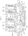
- a semiconductor memory device with a redundant configuration in accordance with this embodiment has a plurality of primary memory cells each of which stores one bit of information, and a plurality of spare memory cells, wherein the whole memory cells are divided into two block groups SA1 and SA2.
- the block groups SA1 and SA2 are each divided into M memory cell blocks (i.e., 2M memory cell blocks (four memory cell blocks a, b, c, and d in this embodiment)).
- the memory cell block a (b, c, d) contains a sense amplifier array 1a (1b, 1c, 1d), a primary memory cell array 3a (3b, 3c, 3d), a row decoder 4a (4b, 4c, 4d), and a column decoder 6a (6b, 6c, 6d).
- a spare memory cell array 2b (2c) is provided which is located next to the primary memory cell array 3b (3c), and the row decoder 4b (4c) is integrated by connecting the primary memory cell to the spare memory cell with a shared decode line.
- Row predecoders 5l and 5r are provided, which send out PREDECODE SIGNALS 10l (for the block group SA1) and 10r (for the block group SA2) respectively to select a primary memory cell corresponding to the address of ADDRESS SIGNAL input.
- Redundancy-use decision circuits 20l and 20r are provided, which store in advance the addresses of defective primary memory cells in each one of the primary memory cell arrays 3a to 3d to send out REDUNDANCY-USE SIGNAL if the address of ADDRESS SIGNAL agrees with the address of the defective primary memory cell stored.
- Redundancy encoders 8l and 8r are provided, which, upon receiving REDUNDANCY-USE SIGNALS from the redundancy-use decision circuits 20l and 20r, send out REDUNDANCY DECODE SIGNALS 11l and 11r to select redundancy memory cells. Further, decode signal selection circuits 9l and 9r are provided which select either the output of the row predecoders 5l and 5r, or the output of the redundancy encoders 8l and 8r.
- the redundancy-use decision circuit 20l (20r) has elements SDl0 to SDln (elements SDr0 to SDrn), the number of which corresponds to the number of primary memory cells (16 primary memory cells here in this embodiment) to be disposed in the block group SA1 (the block group SA2).
- the element SDl0 contains fuses the number of which corresponds to the number of addresses of the primary memory cells arranged in the block group SA2. If a defective memory cell is detected during the examination, a corresponding fuse to the address of the defective memory cell is opened up in advance. Therefore, the address of the defective memory cell can be stored.
- ADDRESS SIGNAL Ak is at a "0"
- this causes the row predecoder 5l, the redundancy-use decision circuit 20r, and the redundancy encoder 8r to operate.
- ADDRESS SIGNAL Ak is at a "1”
- this causes the row predecoder 5r, the redundancy-use decision circuit 20l, and the redundancy encoder 8l to operate.
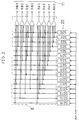
- redundancy encoder 8 The organization of the redundancy encoder 8 is explained by reference to Figure 2. Note that the redundancy encoder 8l is organized in basically the same manner that the redundancy encoder 8r is organized. As show in the figure, the output of 16 elements SD0 to SD15 of the redundancy-use decision circuit 20 receiving ADDRESS SIGNALS A0 to An are translated into REDUNDANCY DECODE SIGNAL 11 comprised of 4 ⁇ 4 MATRIX SIGNALS RA0 to RA3, RB0 to RB3.
- the decode signal selection circuit 9l is supplied with PREDECODE SIGNAL 10l from the row predecoder 5l, and with REDUNDANCY DECODE SIGNAL 11l from the redundancy encoder 8l.
- the decode signal selection circuit 9r is supplied with PREDECODE SIGNAL 10r from the row predecoder 5r, and with REDUNDANCY DECODE SIGNAL 11r from the redundancy encoder 8r.
- these PREDECODE SIGNALS 10l and 10r fed from the row predecoders 5l and 5r, are supplied to the row decoders of one of the block groups SA1 and SA2 that contains the primary memory cell whose address corresponds to the input address, while on the other hand, the outputs of the redundancy encoders 8l and 8r, that is, REDUNDANCY DECODE SIGNALS 11l and 11r are fed to the row decoders belonging to the other block group that contains no primary memory cell whose address corresponds to the input address.
- ADDRESS SIGNAL Ak if ADDRESS SIGNAL Ak is at a "0", the decode signal selection circuit 9l supplies the row decoders 4a and 4b with PREDECODE SIGNAL 10l and the decode signal selection circuit 9r supplies the row decoders 4c and 4d with REDUNDANCY DECODE SIGNAL 11r.
- ADDRESS SIGNAL Ak is at a "1”
- the decode signal selection circuit 9l supplies the row decoders 4a and 4b with REDUNDANCY DECODE SIGNAL 11l and the decode signal selection circuit 9r supplies the row decoders 4c and 4d with PREDECODE SIGNAL 10r.
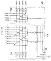
- the row predecoder 5 is made up of three predecoders A, B and C. These predecoders are each provided with four decode lines.
- the decode lines of the predecoder A are combined with the decode lines receiving REDUNDANCY DECODE SIGNAL 11l (MATRIX SIGNALS RA0 to RA3), at each OR gate so that SIGNALS WP0 to WP3 that select primary word lines are sent out.
- the decode lines of the predecoder B are combined with the decode lines receiving REDUNDANCY DECODE SIGNAL 11r (MATRIX SIGNALS RB0 to RB3), at each OR gate so that FIRST GATE VOLTAGE APPLICATION SIGNALS XPA0 to XPA3 are sent out.
- REDUNDANCY DECODE SIGNAL 11r MATRIX SIGNALS RB0 to RB3
- SECOND GATE VOLTAGE APPLICATION SIGNALS XPB0 to XPB3 are sent out.
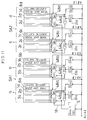
- the row decoder 4 contains a decode circuit 41 in which transistors used to drive the word lines of the primary memory cell array and transistors used to drive the word lines of the spare memory cell array are both arranged in a matrix manner, a word line drive signal generating circuit 21, comprised of elements WD0 to WD3 that send out DRIVE SIGNALS to the decode circuit 41, AND gates 193, and a gate voltage switching circuit 42 that switches, between a "1" and a "0", respective gate voltages of each one of the transistors of the decode circuit 41.
- the word lines of the primary memory cell array and the word lines of the spare memory cell array are connected to the word line drive signal generating circuit 21, through shared decode lines.
- decode signal lines WP0 to WP3 are each supplied with REDUNDANCY DECODE SIGNAL, and at the time when the primary word line is being selected, the WP0 to WP3 are each supplied with PREDECODE SIGNAL.
- a primary word line WLa0 of the memory cell block a contains a defective memory cell, and that the WLa0 is replaced by a spare word line SWc0 of the memory cell block c.
- An address corresponding to the primary word line WLa0 is pre-stored in the element SDr0 of the redundancy-use decision circuit 20r.
- ADDRESS SIGNAL (A0 to Ak) corresponding to the primary word line WLa0 is first fed to the row predecoders 5l and 5r as well as to the redundancy-use decision circuits 20l and 20r.
- the row predecoder 5l and the decision circuit 20r will operate if ADDRESS SIGNAL Ak is at a "0".
- the addresses of the defective memory cells, which are stored in the elements SDr0 to SDrn of the decision circuit 20, are individually compared with this ADDRESS SIGNAL. If the address of ADDRESS SIGNAL input corresponds to the word line WLa0 of the defective memory cell, the element SDr0 of the decision circuit 20 sends out REDUNDANCY SELECTION SIGNAL SWD0.
- the redundancy encoder 8r sends out SIGNALS RA0 and RB0 as REDUNDANCY DECODE SIGNAL.
- the input of the predecoders A to C of the row predecoder 5r becomes a "0".
- REDUNDANCY DECODE SIGNAL 11r only SIGNALS RA0 and RB0 are supplied at a "1".
- PREDECODE SIGNAL WP0 and FIRST GATE VOLTAGE APPLICATION SIGNAL XPA0 become a "1".
- the row decoder 4r shown in Figure 4, a voltage is applied to the element WD0 of the word line drive signal generating circuit 21, and through the AND gates only the spare word lines become a "1", as a whole. From among the spare word lines, a spare word line SWa, which corresponds to the element WD0, is selected.
- the input of the predecoders A to C of the row predecoder 5l becomes a "1". Then the predecoder A sends out, according to the address of the WL0, the predecode signal WP0, the predecoder B sends out FIRST GATE VOLTAGE APPLICATION SIGNAL XAP0, and the predecoder C sends out SECOND GATE VOLTAGE APPLICATION SIGNAL XPB0.
- the input of the word line drive signal generating circuit 21 becomes a "1" and the output of the leftmost AND gate becomes a "1".
- the primary word line WLa0 is selected.
- the element SDr0 of the redundancy-use decision circuit 20 sends out REDUNDANCY-USE SIGNAL (i.e., PRIMARY MEMORY STOP SIGNAL 18l)
- no primary memory cells will be accessed since the primary word line drive signal generating circuit 21 is not operating now.
- the spare word line SWc0 is selected if the primary word line WLa0 contains a defective memory cell. In this way, the word line WLa0 where a defective memory cell is existent is replaced by the spare word line SWc0 to correct the defective memory cell.
- this embodiment makes it possible to replace a primary word line, through which a defective memory cell is accessed, with a spare word line in one of memory cell blocks, whereby the defective word line corrective efficiency becomes increasingly improved, which is shown in Figure 5, comprised of Figure 5a (showing prior art) and Figure 5b (present invention).
- Figure 5a shown prior art
- Figure 5b present invention
- the number of spare word lines is four.
- the WLa0 it is possible for the WLa0 to be replaced by the SWc0, and for the WLa1 by the SWc1. Even if a plurality of defective memory cells are found in one memory cell block in a memory chip, such a memory chip is immune from being defective. The corrective efficiency can be improved, accordingly.
- primary word lines and corresponding spare word lines are provided in different memory cell blocks, so that even if the simultaneous selection of a primary word line and a spare word line takes place, this will not destroy read data. Therefore, the spare word line and the primary word line can be activated, regardless of mutual timing. A high-speed word line activation can be accomplished, accordingly.
- the decode signal selection circuits 9l and 9r are used to feed REDUNDANCY DECODE SIGNAL for selecting the spare word lines SWb0 to SWbn, SWc0 to SWcn to a signal line shared with PREDECODE SIGNAL for selecting the primary word lines WLb1 to WLbm, WLc1 to WLcm.
- the word line drive signal generating circuit 21 is shared. This therefore eliminates needs for the separate provision of primary decode lines and redundancy decode lines, and for the separate provision of a primary word line drive signal generating circuit and a redundancy word line drive signal generating circuit.
- the area of the memory chip can be reduced, in other words, a larger scale integration of semiconductor memory devices can be achieved.
- the redundancy-use decision circuits 20l and 20r, the row predecoder 5l and 5r, and the decode signal selection circuits 9l and 9r are provided. This allows the row decoders 4a to 4d of the memory cell blocks a to d to operate efficiently, and a word line corresponding to the address of ADDRESS SIGNAL can be driven without increasing the memory chip area.
- the invention can be expected to roughly have a double improvement in yield over the conventional redundant system.
- the present invention can be expected to have a five-fold improvement in yield as compared with the conventional redundant system.
- the conventional redundancy system in order to obtain the same yield as the present redundancy system, requires a chip area approximately 5 mm2 greater than that required by the present redundancy system, and as to a 1-gigabit DRAM, the conventional redundant system requires a chip area about 15 mm2 greater than that required by the present redundancy system.
- redundancy encoders 8l and 8r can reduce the number of signal lines for redundancy decode signals. For example, as shown in Figure 2, only eight redundancy decode lines, used to connect MATRIX SIGNALS RA0 to RA3, RB0 to RB3 to 16 REDUNDANCY-USE SIGNALS, are required.
- the first embodiment has been described taking a DRAM with four memory cell blocks as an example, which is not to be considered restrictive. DRAMs, of other types, with a different number of memory cell blocks may be available.
- the decode signal selection circuit 9 is used to feed REDUNDANCY DECODE SIGNAL for selecting a great number of spare word lines to a signal line shared with PREDECODE SIGNAL to share a word line drive signal generating circuit. This effectively produces a chip area reducing effect.
- two of the four memory cell blocks located inside contain spare word lines.
- the variation in memory cell processing is more likely to appear at the outside of a chip than the inside. If a memory cell block with a shorter bit line length including only primary word lines is arranged outside, and a memory cell block with a longer bit line length including spare word line is arranged inside (for instance, arranged around the center of a memory cell array), this realizes a semiconductor memory device that has a long data hold time and a tougher noise-resistance.
- PRIMARY MEMORY STOP SIGNAL 18 brings the operation of the row decoder 4 to a halt. Therefore, no currents are required for selecting and activating the primary word line WL, resulting in achieving less power consumption. Further, since it is unnecessary to get the primary word line WL activated after redundancy-use decision is completed and PRIMARY MEMORY STOP SIGNAL 18 is established, there are no possibilities of a drop in operation speed.
- the defective memory cell is replaced by a spare memory cell in the other memory cell array.
- a defective primary memory cell may be replaced by a spare memory cell in the same memory cell array, and when all spare memory cells are used up a further defective memory cell may be replaced by a spare memory cell in a different memory cell array.
- Figure 6 shows the organization of a semiconductor memory device in accordance with this embodiment.
- the memory cell blocks a to d have the primary memory cell arrays 3a to 3d respectively, and further have the spare memory cell arrays 2a to 2d respectively.
- the row predecoder 5, the redundancy-use decision circuit 20, comprised of the elements SD0 to SDn, the redundancy encoder 8, and a memory cell block selection switching circuit 29 are provided.
- the element SD0 of the redundancy-use decision circuit 20 corresponds to the spare word line SWLa0 of the primary memory cell array 2a, and that an address, corresponding to a primary word line containing a defective memory cell, is stored in advance.
- the row predecoder 5 sends out PREDECODE SIGNAL 10 to select such a primary word line together with PRIMARY BLOCK SELECTION SIGNAL 30.
- the block selection switching circuit 29 Upon receiving PRIMARY BLOCK SELECTION SIGNAL 30, the block selection switching circuit 29 sends out BLOCK SELECTION SIGNAL 32. In this way, the primary word line is selected according to the input address.
- the redundancy-use decision circuit 20 sends out no REDUNDANCY-USE SIGNALS, since the stored address of the defective memory cell disagrees with the input address.
- ADDRESS SIGNAL corresponds to the address of a defective memory cell stored in the element SD0 of the decision circuit 20
- the SD0 sends out REDUNDANCY-USE SIGNAL, and REDUNDANCY DECODE SIGNAL 11 to select the spare word line SWLa0 and REDUNDANCY BLOCK SELECTION SIGNAL 31 are supplied from the redundancy encoder 8.
- PRIMARY MEMORY STOP SIGNAL 18 is fed to the row decoders 4a to 4d so that the primary word lines stop operating.
- the block selection switching circuit 29 translates BLOCK SELECTION SIGNAL 32 from PRIMARY BLOCK SELECTION SIGNAL 30 into REDUNDANCY BLOCK SELECTION SIGNAL 31. Therefore, no primary word lines are subject to selection, the spare word line SWLa0 is selected, and the sense amplifier and the column decoder of the memory cell block a become activated by REDUNDANCY DECODE SIGNAL 11.
- BLOCK SELECTION SIGNAL 32 is switched between PRIMARY BLOCK SELECTION SIGNAL 30 and REDUNDANCY BLOCK SELECTION SIGNAL 31 by the output of the redundancy-use decision circuit 20.
- This makes it possible to replace a primary word line of any memory cell block with a spare word line of any memory cell block. For instance, a defective memory cell is replaced by a spare memory cell in the same memory cell block, and when all spare memory cell are used up a further defective memory cell will be replace by a spare memory cell in a different memory cell block. This results in increasingly improving the spare memory cell availability.
- Figure 7 shows the organization of a semiconductor memory device according to this embodiment.
- This semiconductor memory device includes the memory cell blocks a to d, and the sense amplifiers 1a to 1e, wherein the adjoining memory cell blocks a and b share the sense amplifier 1b, the adjoining memory cell blocks b and c share the sense amplifier 1c, and the adjoining memory cell blocks c and d share the sense amplifier 1d.
- the memory cell block a (b, c, d) has the primary memory cell array 3a (3b, 3c, 3d).
- the leftmost and rightmost memory cell blocks a and d have the spare memory cell arrays 2a and 2d respectively.
- the leftmost memory cell block a has the row decoder 4a that connects the primary memory cell array 3a to the spare memory cell array 2a with a shared decode line.
- the rightmost memory cell block d has the row decoder 4d in which the primary memory cell array 3d and the spare memory cell array 2d are interconnected by a shared decode line.
- the central memory cell blocks b and c have the row decoders 4b and 4c respectively which decode the primary memory cell arrays 3b and 3c respectively.
- Block selection switch arrays 12al to 12dr Intervened between each one of the sense amplifiers 1a to 1e and each one of the memory cell arrays of the memory cell blocks a to d are block selection switch arrays 12al to 12dr. If a primary word line, contained in the primary memory cell array 3b, is selected, selection switches of the block selection switch arrays 12al and 12br are turned on, and switches of the block selection switch arrays 12ar and 12cl are turned off. At the same time, selection switches of the block selection switch arrays 12dl and 12dr, of the primary memory cell array 3d containing a spare word line corresponding to the selected memory cell block, are turned on, and switches of the block selection switch array 12cr are turned off. Other arrangements are the same as the first embodiment (see Figure 1).
- this embodiment can achieve the same remedy efficiency as the first embodiment. Additionally, the pitch of the sense amplifiers 1a to 1e can be reduced, and the number of sense amplifiers can be decreased. This results in a higher density of semiconductor memory devices per chip.
- both the spare memory cell array 2 and the primary memory cell array 3 are arranged in a single memory cell block, wherein the spare memory cell array 2 and the primary memory cell array 3 are connected by a shared decode line in the row decoder 4.
- the row decoder 4 contains the decode circuit 41 in which transistors used to drive the word lines of the primary memory cell array and transistors used to drive the word lines of the spare memory cell array are arranged in a matrix manner, the word line drive signal generating circuit 21, comprised of the elements WD0 to WD3 that send out DRIVE SIGNALS to the decode circuit 41, the AND gates, and the gate voltage switching circuit 42 that switches the respective gate voltages of each one of the primary word line drive transistors of the decode circuit 41, between a "1" and a "0".
- the word line of the primary memory cell array and the word line of the spare memory cell array are connected to the word line drive signal generating circuit 21, through a shared decode line.
- the row predecoder 5 to send out PRECODE SIGNAL 10 upon receiving ADDRESS SIGNAL, a decode signal switching circuit 19, and the redundancy-use decision circuit 20 comprised of the elements SD0 to SD3 are arranged.
- the decode signal switching circuit 19 is supplied with the outputs of the elements SD0 to SD3, and is made up of a stop signal output section 191, comprised of OR elements to send out PRIMARY MEMORY STOP SIGNAL 18 depending upon the operation of the elements SD0 to SD3 of the redundancy-use decision circuit 20, an inverter 192 to invert STOP SIGNAL 18 from the stop signal output section 191, an AND gate 193, comprised of four AND elements that are supplied with the output of the inverter 192 and with PREDECODE SIGNAL 10 fed from the row predecoder 5, and an OR gate 194, comprised of four OR elements that are supplied with the outputs of the elements SD0 to SD3 respectively.
- the output sides of the OR elements of the OR gate 194 are connected through the predecode lines WP0 to WP3 to the elements WD0 to WD3 of the word line drive signal generating circuit 21. Further, the output side of the stop signal output section 191 is connected directly to the gates of the spare word line drive transistors of the decode circuit 41 of the row decoder 4, and is also connected to the gates of the primary word line drive transistors, not directly but through inverters of the gate voltage switching circuit 42.
- the operation of the semiconductor memory device described above is explained.
- the addresses of primary word lines containing defective memory cells are pre-stored in the elements SD0 to SD3 of the redundancy-use decision circuit 20.
- the row predecoder 5 sends out PREDECODE SIGNAL 10 corresponding to the primary word line thus selected. Since the elements SD0 to SD3 do not send out signals at all if the input address disagrees with the stored address in these elements, the stop signal output section 191 sends out no PRIMARY MEMORY STOP SIGNAL 18. Therefore, the output of the inverter 192 becomes a "1". In the AND gate 193, only the AND elements that are supplied with PREDECODE SIGNAL 10 become a "1". The predecode lines WP0 to WP3 are supplied with PREDECODE SIGNAL 10 corresponding to the primary word line at the input address.
- the elements WD0 to WD3 of the word line drive signal generating circuit 21 send out WORD LINE DRIVE SIGNAL.
- the gate voltages of the spare word line drive transistors each come to a "0" state.
- no spare word lines are selected.
- the output of the AND gate 193 connected to a memory cell array at which the primary memory cell corresponding to PREDECODE SIGNAL 10 is placed, becomes a "1". Accordingly, the primary word line, which corresponds to ADDRESS SIGNAL input, is selected.
- the AND gate 193 will not send out PREDECODE SIGNAL 10 but REDUNDANCY-USE SIGNAL, received from the element SD0 of the redundancy-use decision circuit 20, to the predecode line WP0. Because of PRIMARY MEMORY STOP SIGNAL 18 output from the stop signal output section 191, the gate voltages of the transistors connected to the word lines of the spare memory cell array 2 become a "1". This results in selecting the spare word line SWL0.
- the spare memory cell array 2 and the primary memory cell 3 are connected together with a shared decode line. This eliminates a need to provide a dedicated drive signal generating circuit for the spare word lines. The increase of the area of the memory chip due to the arrangement of spare memory cells can be avoided.
- the number of elements of the redundancy-use decision circuit 20 and the number of decode lines of the word line drive signal generating circuit 21 are set even, so that the elements WD0 to WD3 Of the circuit 21 can directly be selected by REDUNDANCY-USE SIGNALS from the elements SD0 to SD3 of the circuit 20. This advantageously simplifies the configuration for decoding a spare memory cell corresponding to the address of a defective memory cell.
- This invention is applicable to a DRAM (Dynamic Random Access Memory) and an SRAM (Static Random Access Memory).
Landscapes
- For Increasing The Reliability Of Semiconductor Memories (AREA)
- Dram (AREA)
- Techniques For Improving Reliability Of Storages (AREA)
Applications Claiming Priority (3)
| Application Number | Priority Date | Filing Date | Title |
|---|---|---|---|
| JP22298/92 | 1992-02-07 | ||
| JP2229892 | 1992-02-07 | ||
| JP2229892 | 1992-02-07 |
Publications (3)
| Publication Number | Publication Date |
|---|---|
| EP0554901A2 true EP0554901A2 (de) | 1993-08-11 |
| EP0554901A3 EP0554901A3 (de) | 1998-02-11 |
| EP0554901B1 EP0554901B1 (de) | 2000-05-17 |
Family
ID=12078840
Family Applications (1)
| Application Number | Title | Priority Date | Filing Date |
|---|---|---|---|
| EP93101850A Expired - Lifetime EP0554901B1 (de) | 1992-02-07 | 1993-02-05 | Halbleiterspeicheranordnung mit Ersatzspeicherzellen |
Country Status (5)
| Country | Link |
|---|---|
| US (1) | US5475648A (de) |
| EP (1) | EP0554901B1 (de) |
| JP (1) | JP3040625B2 (de) |
| KR (1) | KR960004741B1 (de) |
| DE (1) | DE69328639T2 (de) |
Cited By (3)
| Publication number | Priority date | Publication date | Assignee | Title |
|---|---|---|---|---|
| EP0660237A3 (de) * | 1993-12-22 | 1997-02-19 | Hitachi Ltd | Halbleiterspeichergerät mit einem Ersatzspeicherzellfeld. |
| EP0890902A3 (de) * | 1997-07-10 | 1999-09-22 | Siemens Aktiengesellschaft | Redundanzschaltung für Halbleiterspeicher |
| WO2003043023A1 (de) * | 2001-11-12 | 2003-05-22 | Martin Rieger | Verfahren zur rekonfiguration eines speichers |
Families Citing this family (42)
| Publication number | Priority date | Publication date | Assignee | Title |
|---|---|---|---|---|
| JPH07282597A (ja) * | 1994-04-12 | 1995-10-27 | Mitsubishi Electric Corp | 半導体記憶装置 |
| KR0152168B1 (ko) * | 1994-04-15 | 1998-10-01 | 모리시다 요이치 | 반도체 기억장치 |
| US5901105A (en) * | 1995-04-05 | 1999-05-04 | Ong; Adrian E | Dynamic random access memory having decoding circuitry for partial memory blocks |
| DE59510285D1 (de) * | 1995-08-09 | 2002-08-22 | Infineon Technologies Ag | Integrierter Halbleiterspeicher mit Redundanzspeicherzellen |
| JP3557019B2 (ja) * | 1995-11-17 | 2004-08-25 | 株式会社東芝 | 半導体記憶装置 |
| US5671185A (en) * | 1996-03-12 | 1997-09-23 | United Microelectronics Corporation | Apparatus for replacing defective cells in a memory device |
| JP3220009B2 (ja) * | 1996-05-30 | 2001-10-22 | 日本電気株式会社 | 半導体記憶装置 |
| US5699307A (en) * | 1996-06-28 | 1997-12-16 | Intel Corporation | Method and apparatus for providing redundant memory in an integrated circuit utilizing a subarray shuffle replacement scheme |
| US5781717A (en) * | 1996-09-19 | 1998-07-14 | I-Cube, Inc. | Dynamic spare column replacement memory system |
| US5996106A (en) | 1997-02-04 | 1999-11-30 | Micron Technology, Inc. | Multi bank test mode for memory devices |
| US5841710A (en) * | 1997-02-14 | 1998-11-24 | Micron Electronics, Inc. | Dynamic address remapping decoder |
| JP3476646B2 (ja) * | 1997-03-07 | 2003-12-10 | シャープ株式会社 | 半導体記憶装置 |
| US5831913A (en) * | 1997-03-31 | 1998-11-03 | International Business Machines Corporation | Method of making a memory fault-tolerant using a variable size redundancy replacement configuration |
| US5831914A (en) * | 1997-03-31 | 1998-11-03 | International Business Machines Corporation | Variable size redundancy replacement architecture to make a memory fault-tolerant |
| US5913928A (en) * | 1997-05-09 | 1999-06-22 | Micron Technology, Inc. | Data compression test mode independent of redundancy |
| US5978931A (en) * | 1997-07-16 | 1999-11-02 | International Business Machines Corporation | Variable domain redundancy replacement configuration for a memory device |
| US5881003A (en) * | 1997-07-16 | 1999-03-09 | International Business Machines Corporation | Method of making a memory device fault tolerant using a variable domain redundancy replacement configuration |
| JP3507674B2 (ja) * | 1997-10-30 | 2004-03-15 | 株式会社東芝 | 半導体記憶装置 |
| US5970000A (en) * | 1998-02-02 | 1999-10-19 | International Business Machines Corporation | Repairable semiconductor integrated circuit memory by selective assignment of groups of redundancy elements to domains |
| US6081463A (en) * | 1998-02-25 | 2000-06-27 | Micron Technology, Inc. | Semiconductor memory remapping |
| US6314527B1 (en) | 1998-03-05 | 2001-11-06 | Micron Technology, Inc. | Recovery of useful areas of partially defective synchronous memory components |
| US6332183B1 (en) | 1998-03-05 | 2001-12-18 | Micron Technology, Inc. | Method for recovery of useful areas of partially defective synchronous memory components |
| TW582041B (en) * | 1998-04-17 | 2004-04-01 | Siemens Ag | Memory-arrangement with redundant memory-cells and method to access on the redundant memory-cells |
| US6381707B1 (en) | 1998-04-28 | 2002-04-30 | Micron Technology, Inc. | System for decoding addresses for a defective memory array |
| US6381708B1 (en) | 1998-04-28 | 2002-04-30 | Micron Technology, Inc. | Method for decoding addresses for a defective memory array |
| JP2000011681A (ja) | 1998-06-22 | 2000-01-14 | Mitsubishi Electric Corp | 同期型半導体記憶装置 |
| US5978291A (en) * | 1998-09-30 | 1999-11-02 | International Business Machines Corporation | Sub-block redundancy replacement for a giga-bit scale DRAM |
| JP2000149564A (ja) | 1998-10-30 | 2000-05-30 | Mitsubishi Electric Corp | 半導体記憶装置 |
| US6018483A (en) * | 1998-12-10 | 2000-01-25 | Siemens Aktiengesellschaft | Distributed block redundancy for memory devices |
| US6496876B1 (en) | 1998-12-21 | 2002-12-17 | Micron Technology, Inc. | System and method for storing a tag to identify a functional storage location in a memory device |
| JP2000243086A (ja) | 1998-12-24 | 2000-09-08 | Mitsubishi Electric Corp | 半導体記憶装置 |
| JP3964584B2 (ja) * | 1999-11-26 | 2007-08-22 | 東芝マイクロエレクトロニクス株式会社 | 半導体記憶装置 |
| US6578157B1 (en) | 2000-03-06 | 2003-06-10 | Micron Technology, Inc. | Method and apparatus for recovery of useful areas of partially defective direct rambus rimm components |
| US7269765B1 (en) | 2000-04-13 | 2007-09-11 | Micron Technology, Inc. | Method and apparatus for storing failing part locations in a module |
| JP4679036B2 (ja) * | 2002-09-12 | 2011-04-27 | ルネサスエレクトロニクス株式会社 | 記憶装置 |
| CN1823392A (zh) * | 2003-07-15 | 2006-08-23 | 尔必达存储器株式会社 | 半导体存储器件 |
| DE10335708B4 (de) * | 2003-08-05 | 2009-02-26 | Qimonda Ag | Hub-Baustein zum Anschließen von einem oder mehreren Speicherbausteinen |
| US7134057B1 (en) | 2004-02-13 | 2006-11-07 | Sun Microsystems, Inc. | Off-pitch column redundancy using dynamic shifters |
| KR100557712B1 (ko) * | 2004-11-10 | 2006-03-07 | 삼성전자주식회사 | 반도체 메모리의 리페어 방법 및 장치 |
| JP2007172832A (ja) * | 2007-03-20 | 2007-07-05 | Renesas Technology Corp | 半導体記憶装置及び半導体記憶装置の欠陥救済方法 |
| JP2011159345A (ja) * | 2010-01-29 | 2011-08-18 | Elpida Memory Inc | 半導体記憶装置 |
| KR20170055222A (ko) | 2015-11-11 | 2017-05-19 | 삼성전자주식회사 | 리페어 단위 변경 기능을 가지는 메모리 장치 및 메모리 시스템 |
Family Cites Families (19)
| Publication number | Priority date | Publication date | Assignee | Title |
|---|---|---|---|---|
| US4346459A (en) * | 1980-06-30 | 1982-08-24 | Inmos Corporation | Redundancy scheme for an MOS memory |
| JPH0670880B2 (ja) * | 1983-01-21 | 1994-09-07 | 株式会社日立マイコンシステム | 半導体記憶装置 |
| JPS62125598A (ja) * | 1985-11-27 | 1987-06-06 | Hitachi Ltd | 欠陥救済回路 |
| JPS62293598A (ja) * | 1986-06-12 | 1987-12-21 | Toshiba Corp | 半導体記憶装置 |
| JP2587973B2 (ja) * | 1987-07-13 | 1997-03-05 | 日本電信電話株式会社 | 冗長構成半導体メモリ |
| JP2590897B2 (ja) * | 1987-07-20 | 1997-03-12 | 日本電気株式会社 | 半導体メモリ |
| JPS6437797A (en) * | 1987-08-03 | 1989-02-08 | Oki Electric Ind Co Ltd | Eprom device |
| JP2776835B2 (ja) * | 1988-07-08 | 1998-07-16 | 株式会社日立製作所 | 欠陥救済用の冗長回路を有する半導体メモリ |
| JPH02113490A (ja) * | 1988-10-21 | 1990-04-25 | Hitachi Ltd | 半導体記憶装置 |
| KR910005601B1 (ko) * | 1989-05-24 | 1991-07-31 | 삼성전자주식회사 | 리던던트 블럭을 가지는 반도체 메모리장치 |
| US5058070A (en) * | 1990-02-12 | 1991-10-15 | Motorola, Inc. | High speed memory with row redundancy |
| US5126973A (en) * | 1990-02-14 | 1992-06-30 | Texas Instruments Incorporated | Redundancy scheme for eliminating defects in a memory device |
| US5270976A (en) * | 1990-06-19 | 1993-12-14 | Texas Instruments Incorporated | Laser link decoder for DRAM redundancy scheme |
| JP3019869B2 (ja) * | 1990-10-16 | 2000-03-13 | 富士通株式会社 | 半導体メモリ |
| JP2629463B2 (ja) * | 1991-01-25 | 1997-07-09 | 日本電気株式会社 | 半導体記憶回路 |
| US5255227A (en) * | 1991-02-06 | 1993-10-19 | Hewlett-Packard Company | Switched row/column memory redundancy |
| JP2730375B2 (ja) * | 1992-01-31 | 1998-03-25 | 日本電気株式会社 | 半導体メモリ |
| US5257229A (en) * | 1992-01-31 | 1993-10-26 | Sgs-Thomson Microelectronics, Inc. | Column redundancy architecture for a read/write memory |
| US5295101A (en) * | 1992-01-31 | 1994-03-15 | Texas Instruments Incorporated | Array block level redundancy with steering logic |
-
1993
- 1993-01-26 JP JP05010916A patent/JP3040625B2/ja not_active Expired - Lifetime
- 1993-02-04 US US08/013,382 patent/US5475648A/en not_active Expired - Lifetime
- 1993-02-05 EP EP93101850A patent/EP0554901B1/de not_active Expired - Lifetime
- 1993-02-05 DE DE69328639T patent/DE69328639T2/de not_active Expired - Lifetime
- 1993-02-06 KR KR1019930001613A patent/KR960004741B1/ko not_active Expired - Lifetime
Cited By (4)
| Publication number | Priority date | Publication date | Assignee | Title |
|---|---|---|---|---|
| EP0660237A3 (de) * | 1993-12-22 | 1997-02-19 | Hitachi Ltd | Halbleiterspeichergerät mit einem Ersatzspeicherzellfeld. |
| EP0890902A3 (de) * | 1997-07-10 | 1999-09-22 | Siemens Aktiengesellschaft | Redundanzschaltung für Halbleiterspeicher |
| US6188617B1 (en) | 1997-07-10 | 2001-02-13 | Infineon Technologies Ag | Reundancy circuit for semiconductor memories |
| WO2003043023A1 (de) * | 2001-11-12 | 2003-05-22 | Martin Rieger | Verfahren zur rekonfiguration eines speichers |
Also Published As
| Publication number | Publication date |
|---|---|
| US5475648A (en) | 1995-12-12 |
| KR930018593A (ko) | 1993-09-22 |
| DE69328639T2 (de) | 2000-08-31 |
| EP0554901B1 (de) | 2000-05-17 |
| DE69328639D1 (de) | 2000-06-21 |
| KR960004741B1 (ko) | 1996-04-12 |
| JP3040625B2 (ja) | 2000-05-15 |
| EP0554901A3 (de) | 1998-02-11 |
| JPH05282894A (ja) | 1993-10-29 |
Similar Documents
| Publication | Publication Date | Title |
|---|---|---|
| US5475648A (en) | Redundancy semiconductor memory device which utilizes spare memory cells from a plurality of different memory blocks, and utilizes the same decode lines for both the primary and spare memory cells | |
| US5126973A (en) | Redundancy scheme for eliminating defects in a memory device | |
| KR100392557B1 (ko) | 반도체장치,컴퓨터시스템 및 액세스방법 | |
| US5060197A (en) | Static random access memory with redundancy | |
| US5617364A (en) | Semiconductor memory device | |
| US5208782A (en) | Semiconductor integrated circuit device having a plurality of memory blocks and a lead on chip (LOC) arrangement | |
| US6735104B2 (en) | Memory device with row and column decoder circuits arranged in a checkerboard pattern under a plurality of memory arrays | |
| US6094382A (en) | Integrated circuit memory devices with improved layout of fuse boxes and buses | |
| EP0142127B1 (de) | Redundante Schaltung für ein Halbleiterspeichergerät | |
| US6055196A (en) | Semiconductor device with increased replacement efficiency by redundant memory cell arrays | |
| KR100529706B1 (ko) | 반도체 기억장치 | |
| US6490210B2 (en) | Semiconductor memory integrated circuit employing a redundant circuit system for compensating for defectiveness | |
| US4554646A (en) | Semiconductor memory device | |
| US3715735A (en) | Segmentized memory module and method of making same | |
| US6351413B1 (en) | Nonvolatile memory device, in particular a flash-EEPROM | |
| US5787043A (en) | Semiconductor memory device having a redundancy capability | |
| US5970002A (en) | Semiconductor memory device having redundancy function | |
| US6208569B1 (en) | Method of and apparatus for sharing redundancy circuits between memory arrays within a semiconductor memory device | |
| KR0140350B1 (ko) | 반도체 기억 장치 | |
| US6954398B2 (en) | Semiconductor memory device including subword drivers | |
| KR19990023677A (ko) | 용장 회로를 구비한 반도체 기억 장치 | |
| KR960001859B1 (ko) | 반도체 메모리장치의 디코딩회로 및 그 방법 | |
| US6185146B1 (en) | Semiconductor memory device and method for producing the same | |
| KR100285099B1 (ko) | 반도체기억장치의결함구제회로 | |
| US6473872B1 (en) | Address decoding system and method for failure toleration in a memory bank |
Legal Events
| Date | Code | Title | Description |
|---|---|---|---|
| PUAI | Public reference made under article 153(3) epc to a published international application that has entered the european phase |
Free format text: ORIGINAL CODE: 0009012 |
|
| AK | Designated contracting states |
Kind code of ref document: A2 Designated state(s): DE FR GB |
|
| PUAL | Search report despatched |
Free format text: ORIGINAL CODE: 0009013 |
|
| AK | Designated contracting states |
Kind code of ref document: A3 Designated state(s): DE FR GB |
|
| 17P | Request for examination filed |
Effective date: 19980526 |
|
| 17Q | First examination report despatched |
Effective date: 19980925 |
|
| GRAG | Despatch of communication of intention to grant |
Free format text: ORIGINAL CODE: EPIDOS AGRA |
|
| RTI1 | Title (correction) |
Free format text: SEMICONDUCTOR MEMORY DEVICE WITH SPARE MEMORY CELLS |
|
| GRAG | Despatch of communication of intention to grant |
Free format text: ORIGINAL CODE: EPIDOS AGRA |
|
| GRAH | Despatch of communication of intention to grant a patent |
Free format text: ORIGINAL CODE: EPIDOS IGRA |
|
| GRAH | Despatch of communication of intention to grant a patent |
Free format text: ORIGINAL CODE: EPIDOS IGRA |
|
| GRAA | (expected) grant |
Free format text: ORIGINAL CODE: 0009210 |
|
| AK | Designated contracting states |
Kind code of ref document: B1 Designated state(s): DE FR GB |
|
| REF | Corresponds to: |
Ref document number: 69328639 Country of ref document: DE Date of ref document: 20000621 |
|
| ET | Fr: translation filed | ||
| PLBE | No opposition filed within time limit |
Free format text: ORIGINAL CODE: 0009261 |
|
| STAA | Information on the status of an ep patent application or granted ep patent |
Free format text: STATUS: NO OPPOSITION FILED WITHIN TIME LIMIT |
|
| 26N | No opposition filed | ||
| REG | Reference to a national code |
Ref country code: GB Ref legal event code: IF02 |
|
| PGFP | Annual fee paid to national office [announced via postgrant information from national office to epo] |
Ref country code: FR Payment date: 20120221 Year of fee payment: 20 |
|
| PGFP | Annual fee paid to national office [announced via postgrant information from national office to epo] |
Ref country code: DE Payment date: 20120131 Year of fee payment: 20 |
|
| PGFP | Annual fee paid to national office [announced via postgrant information from national office to epo] |
Ref country code: GB Payment date: 20120201 Year of fee payment: 20 |
|
| REG | Reference to a national code |
Ref country code: DE Ref legal event code: R071 Ref document number: 69328639 Country of ref document: DE |
|
| REG | Reference to a national code |
Ref country code: GB Ref legal event code: PE20 Expiry date: 20130204 |
|
| PG25 | Lapsed in a contracting state [announced via postgrant information from national office to epo] |
Ref country code: GB Free format text: LAPSE BECAUSE OF EXPIRATION OF PROTECTION Effective date: 20130204 Ref country code: DE Free format text: LAPSE BECAUSE OF EXPIRATION OF PROTECTION Effective date: 20130206 |