EP0555832B1 - Méthode et appareil de modulation et méthode et appareil de démodulation - Google Patents
Méthode et appareil de modulation et méthode et appareil de démodulation Download PDFInfo
- Publication number
- EP0555832B1 EP0555832B1 EP93102075A EP93102075A EP0555832B1 EP 0555832 B1 EP0555832 B1 EP 0555832B1 EP 93102075 A EP93102075 A EP 93102075A EP 93102075 A EP93102075 A EP 93102075A EP 0555832 B1 EP0555832 B1 EP 0555832B1
- Authority
- EP
- European Patent Office
- Prior art keywords
- data
- rule
- code
- modulating
- accordance
- Prior art date
- Legal status (The legal status is an assumption and is not a legal conclusion. Google has not performed a legal analysis and makes no representation as to the accuracy of the status listed.)
- Expired - Lifetime
Links
Images



Classifications
-
- G—PHYSICS
- G11—INFORMATION STORAGE
- G11B—INFORMATION STORAGE BASED ON RELATIVE MOVEMENT BETWEEN RECORD CARRIER AND TRANSDUCER
- G11B20/00—Signal processing not specific to the method of recording or reproducing; Circuits therefor
- G11B20/10—Digital recording or reproducing
- G11B20/14—Digital recording or reproducing using self-clocking codes
- G11B20/1403—Digital recording or reproducing using self-clocking codes characterised by the use of two levels
- G11B20/1423—Code representation depending on subsequent bits, e.g. delay modulation, double density code, Miller code
- G11B20/1426—Code representation depending on subsequent bits, e.g. delay modulation, double density code, Miller code conversion to or from block codes or representations thereof
-
- H—ELECTRICITY
- H03—ELECTRONIC CIRCUITRY
- H03M—CODING; DECODING; CODE CONVERSION IN GENERAL
- H03M5/00—Conversion of the form of the representation of individual digits
- H03M5/02—Conversion to or from representation by pulses
- H03M5/04—Conversion to or from representation by pulses the pulses having two levels
- H03M5/14—Code representation, e.g. transition, for a given bit cell depending on the information in one or more adjacent bit cells, e.g. delay modulation code, double density code
- H03M5/145—Conversion to or from block codes or representations thereof
Definitions
- This invention relates to a data modulating method and apparatus and a data demodulating method and apparatus suitable for use for digitally recording data onto a record medium, and more particularly to a data modulating method and apparatus and a data demodulating method and apparatus wherein a modulated code in the form of a variable length code is used and record data in units of m bits are converted into a channel code in units of n bits.
- a signal In a magnetic recording system, generally a signal has a differentiation frequency characteristic and suffers from deterioration in a high frequency band. This arises from a loss at a head gap, a loss by a space between a head and a record medium, a loss originating in thickness of a record medium, a low frequency band loss at a rotary transformer and so forth. Further, noise such as crosstalk noise from an adjacent track, noise from a record medium and overwrite noise could make a cause of a random error. In order to record and reproduce data accurately irrespective of such losses and noise, digital information should be recorded onto a record medium after it is modulated so that it may be compatible with a recording system, which allows a greater amount of information to be recorded stably. To this end, channel coding of data is performed in accordance with a predetermined rule.
- the block coding involves dividing a data sequence into blocks of m x i bits and converting each data word into a channel code of n x i channel bits in accordance with a suitable coding rule.
- i 1
- the channel code is a fixed length code, but when i is greater than 1 and the binding length r is greater than 1, the channel code is a variable length code.
- the block code is also called (d, k;m, n;r) code.
- d is a minimum run number of 0 while k is a maximum run number of 0.
- the block coding is disclosed in Japanese Patent Laid-Open Application No. Heisei 01-221919, laid open on September 5, 1989, under the title of "Variable Length Code Converting Method".
- the run numbers of 0 at the beginning and last ends of a code word are restricted and a decisively decodable code word is selected. Consequently, a code having a minimum magnetization reversal distance (Tmin) which is 1.33 times that of a conventional (2, 7) RLL code and is twice that of the MFM.
- the run number of "0" of a binary code word train of continuous code words after conversion is restricted equal to or greater than 5 but equal to or smaller than 16 (d, k).
- variable length code to be used as a code word
- the requirements for such variable length code to be used as a code word include three requirements that the (d, k) restriction is satisfied within one code word, that the (d, k) restriction is satisfied when code words are connected to each other, and that a boundary of a code word can be discriminated correctly and can be decoded decisively, and an additional requirement that code words are allotted preferentially from that one which includes a greatest number of "1s" so that the average magnetization reversal distance may be minimized.
- variable length code disclosed in the prior art documents is disadvantageous in that, when compared with the variable length code employed in the present invention, the detecting window width Tw is narrower and the detecting efficiency upon decoding is lower.
- binary data are outputted successively in synchronism with a clock signal to terminals for parallel outputs of a serial/parallel register of 10 bits.
- a coder receives, at input terminals thereof, the data from the output terminals of the serial/parallel register, generates a 5-bit conversion code in accordance with a coding algorithm, and outputs it to a 5-bit output terminal.
- the 5-bit conversion code is inputted to a 5-bit serial/parallel resistor, from which a conversion code train is outputted to an output terminal of it.
- the coding method does not involve a variable length code but involves a fixed length code, and employs a code resembling the variable length code employed in the present invention.
- the algorithm of the generating method of the code is complicated, and accordingly, also the hardware configuration is complicated.
- a further block coding technique is disclosed in "Proposal of (3, 19;4, 9;3) Code", Collection of Theses of Spring National Conference of Electronic Information Communication Society, 1989, which describes a (3, 19;4, 9;3) code as a concrete example of a (3, k) variable length code.
- the code is superior in minimum magnetization reversal distance (Tmin) to the (2, 7) RLL code or the 2/3 code and is superior in Tmin x Tw (minimum magnetization reversal distance x detecting window width) to the (2, 7) RLL code.
- a fixed length code sometimes employs a dummy code in order to adjust the code length, and has a subject in that data cannot be recorded in a high density.
- a variable length code does not use a dummy code, and accordingly, higher density recording is allowed.
- a variable length code has a subject in that a dc component cannot be controlled.
- variable length channel codes in which a sequence of j consecutive data words (blocks) of m bits is mapped by a conversion table into channel code words of j x n bits, where 1 ⁇ j ⁇ r. These codes allow a high recording density.
- the sequence of encoded binary digits consists of a plurality of binary digit blocks, each of which is formed with a predetermined number of the encoded binary digits obtained from the binary data and redundant codes, each of which is inserted between each successive two of the binary digit blocks and can produce the recording signal forming a rectangular pulse train with a waveform which has a long minimum run length and does not contain a Dc-component or containes a reduced Dc-component when it is NRZI-modulated.
- a coding apparatus to which the present invention is applied.
- the coding apparatus is generally constructed such that recording data are supplied to read only memories (ROMs) 1 to 3 so that they may be coded in accordance with conversion tables 1 to 3 stored in the ROMs 1 to 3, respectively.
- Codes outputted from the ROMs 1 and 2 are supplied to a multiplexer (MUX) 6.
- MUX multiplexer
- a further code outputted from the ROM 3 is supplied to the multiplexer 6 by way of another multiplexer (MUX) 5.
- a dc management circuit 4 calculates a dc component of the inputted recording data and controls the multiplexer 5 in accordance with a result of the calculation.
- the multiplexer 6 selects one of codes supplied thereto from the ROMS 1 and 2 and the multiplexer 5 and outputs the selected code to the multiplexer 7. Also a synchronizing signal (SYNC) is supplied from a circuit not shown to the multiplexer 7. The multiplexer 7 selects a code supplied thereto from the multiplexer 6 or the synchronizing signal and outputs it as modulated data to a circuit not shown.
- a timing management circuit 8 monitors inputted recording data and controls the multiplexers 6 and 7 at a predetermined timing.
- the table 1 shown in Fig. 2 is stored in the ROM 1.
- the table 1 serves as a conversion table for converting input recording data into a (1, 7;2, 3;4) code.
- each recording data of 2, 4, 6 or 8 bits shown on the left side in Fig. 2 is converted into a channel code of 3, 6, 9 or 12 bits shown on the right side in Fig. 2 in accordance with the table 1.
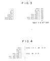
- Fig. 3 shows the table 2 stored in the ROM 2.
- Each recording data of 2, 4 or 6 bits on the left side in Fig. 3 is converted into a channel code of 3, 6 or 9 bits shown on the right side in Fig. 3 in accordance with the table 3.
- a code according to the table 3 which will be hereinafter described is not added, one 0 of one bit is added to each channel code.
- the table 1 shown in Fig. 2 converts recording data at a portion other than a boundary portion of a block as a unit of processing of recording data
- the table 2 shown in Fig. 3 converts recording data at the boundary portion of the block.
- the 2-bit data of the former half is either 01 or 00.
- the boundary is reached at the fourth bit in the former half of recording data of 6 bits, the data at the boundary is either 0001 or 0000.
- the boundary is reached at the sixth bit in the former half of recording data of 8 bits, the data at the boundary is either 000001 or 000000.
- recording data at the boundary presents a total of eight values shown on the left side in Fig. 3.
- the eight different data are converted into corresponding channel codes indicated on the respective right sides of them.
- the table 3 shown in Fig. 4 is stored in the ROM 3.
- the values indicated on the left side in Fig. 4 correspond to the values indicated on the right side in the table 2 of Fig. 3.
- the code of 000 or 010 is added. Which one of 000 or 010 is to be added is determined so that a dc component may be minimized. It is to be noted that, in this instance, the value 000 may be replaced by 101.
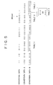
- the multiplexer 6 is changed over to the ROM 2 side. Consequently, data 101001 indicated as conversion data B in Fig. 5 are obtained as the conversion data obtained by conversion of the recording data 0000 in accordance with the table 2 and are outputted as modulated data by way of the multiplexers 6 and 7. Subsequently, the dc management circuit 4 calculates a digital sum variation (DSV) corresponding to the recording data till then and causes the multiplexer 5 to select either 010 or 000 from the ROM 3 in accordance with a result of the calculation so that the selected data 010 or 000 may be outputted as modulated data by way of the multiplexers 6 and 7.
- DSV digital sum variation
- the remaining data 0111 of the recording data is converted as first data of the next block into the code of 001000 as the conversion code A in accordance with the rule of the table 1 of the ROM 1. Succeeding recording data are thereafter coded in a similar manner.
- the values of the data A 1 to A 3 are determined in the following manner.
- the value (000 (non-reverse) or 010 (reverse)) is determined taking the value a1 of the digital sum variation till A 1 and the value f 2 of the digital sum variation of the code C 2 into consideration.
- the reverse value (010) is selected, but if they have different signs (one of them is positive and the other is negative), the non-reverse value (000 or 101) is selected.
- the values a 2 and f 3 have a same sign, the value A 2 is set to 010, but if they have different signs, the value A 2 is set to 000 or 101.
- values of the digital sum variation of the value a 2 are calculated applying all of the values stored as the value A 1 in the table 3 (the digital sum variation of the value A 1 is represented by t 1 ), and one of the thus calculated values which exhibits the smallest value among them is adopted as the value A 1 .
- the value a 2 is calculated applying 000 as the value A 1
- the value a 2 is calculated applying 010. Further, the thus calculated two values are compared with each other, and one of them which presents a smaller value is selected as the value a 2 .
- the value a 3 is calculated applying 000 as the value A 2 , and then the value a 3 is calculated applying 010. Then, the thus calculated two values are compared with each other, and one of them which presents a smaller value is selected as the value A 2 .
- the hardware configuration is complicated comparing with another configuration in which a fixed non-reverse condition is adopted, but the value of the digital sum variation can be minimized.
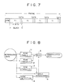
- Fig. 7 illustrates a signal format of a code obtained in this manner.
- one frame is constituted from four blocks, and a synchronizing signal is added to the top of the frame.
- Each of the blocks is constituted from a code T 1 obtained by conversion in accordance with the table 1, another code T 2 obtained by conversion in accordance with the table 2, and a further code T 3 obtained by conversion in accordance with the table 3.
- the codes T 1 and T 2 are codes of original data and the code T 3 is a code of control bits. Accordingly, if the codes T 1 and T 2 have a total of X bits and the code T 3 has Y bits, then the redundancy in the present format is given by Y/(X + Y).
- Fig. 8 shows an example of configuration of a decoding apparatus which demodulates data obtained by modulation by the apparatus shown in Fig. 1.
- the decoding apparatus shown is generally constructed such that a reverse converting circuit for tables 1 and 2 (a circuit for converting codes on the right side into code on the left side of Figs. 2 and 3) is constituted from ROMs 11, 12 and 13, in which the tables 1, 2, 3 which are identical with the tables 1, 2 and 3 in the ROMs 1, 2 and 3 of the modulating apparatus of Fig. 1, respectively, are stored, respectively.
- a synchronizing signal detecting circuit 14 detects a synchronizing signal from reproduced data and supplies such detection signal to a timing management circuit 16.
- the timing management circuit 16 monitors the input reproduced data and an output of the synchronizing signal detecting circuit 14 and controls a multiplexer circuit 15 at a predetermined timing.
- the timing management circuit 16 controls the multiplexer 15 so that the output of the ROM 11 may be selected.
- the timing management circuit 16 controls the multiplexer 15 so that the output of the ROM 12 may be selected.
- the timing management circuit 16 controls the multiplexer 15 so that the reproduced data may not be outputted. Demodulated data are obtained from the multiplexer 15 in this manner.
- tables 1 to 3 are used in combination in the coding and decoding apparatus described above, alternatively the tables 1 and 2 or the tables 1 and 3 may be used in combination.
Landscapes
- Engineering & Computer Science (AREA)
- Signal Processing (AREA)
- Theoretical Computer Science (AREA)
- Signal Processing For Digital Recording And Reproducing (AREA)
- Compression, Expansion, Code Conversion, And Decoders (AREA)
Claims (8)
- Procédé de modulation de données destiné à moduler des données d'enregistrement en un code de canal à longueur variable en convertissant des codes données de m . r bits en codes de canal de n . r bits, n étant supérieur à m, r définissant la longueur variable des codes de canal, et la longueur ainsi que la règle de conversion étant déterminées par une table de conversion,caractérisé par les étapes consistant à:diviser les données d'enregistrement en blocs,moduler les données d'enregistrement à l'intérieur d'une partie d'un bloc autre qu'une partie de limite des blocs en des premiers codes de canal conformément à une première règle, et moduler les données restantes au niveau de la limite en un second mot de canal conformément à une seconde règle différente de la première règle,dans lequel un code de commande destiné à minimiser une composante en courant continu est ajouté au second mot de canal conformément à une troisième règle.
- Procédé de modulation de données selon la revendication 1, dans lequel la troisième règle définit l'addition du code de commande sur la base d'une valeur de variation de somme numérique (a1) à la fin d'un bloc prédéterminé (c1) et la valeur de variation de somme numérique (f2) d'un bloc suivant (c2).
- Procédé de modulation de données selon la revendication 2, dans lequel un code parmi une pluralité de codes de commande préparés à l'avance est ajouté de façon à minimiser la valeur de variation de somme numérique jusqu'au bloc suivant qui suit le bloc prédéterminé.
- Procédé de démodulation de données destiné à démoduler un code de canal qui peut être obtenu par le procédé de la revendication 1, comprenant les étapes consistant à:démoduler des codes de canal à l'intérieur d'une partie autre qu'une partie de limite de chacun des blocs conformément à une première règle, et démoduler le code de canal restant au niveau de la partie de limite du bloc conformément à une seconde règle différente de la première règle, dans lequelun code de commande ajouté lors de la modulation pour pouvoir minimiser une composante en courant continu est éliminé du code modulé.
- Dispositif de modulation de données destiné à moduler des données d'enregistrement en un code de canal à longueur variable en convertissant des codes de données de m . r bits en codes de canal de n . r bits, n étant supérieur à m, r définissant la longueur variable des codes de canal, et la longueur ainsi que la règle de conversion étant déterminées par une table de conversion,caractérisé parun premier moyen de mémorisation (1) destiné à mémoriser une première table de conversion utilisée pour moduler des données d'enregistrement à l'intérieur d'une partie autre qu'une partie de limite des blocs en un code de canal conformément à une première règle,un second moyen de mémorisation (2) destiné à mémoriser une seconde table de conversion utilisée pour moduler les données restantes au niveau de la partie de limite de chaque bloc en un code de canal conformément à une seconde règle différente de la première règle,un moyen de multiplexeur (6) destiné à multiplexer des sorties desdits premier (1) et second (2) moyens de modulation,un moyen de gestion du cadencement (8) destiné à commander le moyen de multiplexage en réponse aux données d'enregistrement reçues, etun moyen de pilotage de la composante continue (3, 4, 5) destiné à ajouter un code de commande en vue de minimiser une composante de courant continu conformément à une troisième règle, à un code de canal obtenu par une modulation conforme à la seconde règle.
- Dispositif de modulation de données selon la revendication 5, dans lequel la troisième règle définit une addition du code de commande sur la base d'une valeur de variation de somme numérique à la fin d'un bloc prédéterminé et la valeur de variation de somme numérique d'un bloc suivant.
- Dispositif de modulation de données selon la revendication 6, dans lequel ledit moyen de pilotage de la composante continue (3, 4, 5) ajoute celui, parmi la pluralité de codes de commande préparés à l'avance, qui minimise la valeur de variation de la somme numérique jusqu'au bloc suivant qui suit le bloc prédéterminé.
- Dispositif de démodulation de données destiné à démoduler un code de canal qui peut être obtenu grâce au procédé selon la revendication 1 ou le dispositif selon la revendication 5, comprenantun premier moyen de mémorisation (11) destiné à mémoriser une première table de conversion afin de démoduler des codes de canal à l'intérieur d'une partie autre qu'une partie de limite de chacun des blocs conformément à une première règle,un second moyen de mémorisation (12) destiné à mémoriser une seconde table de conversion afin de démoduler la partie restante du code modulé au niveau de la partie de limite de chaque bloc conformément à une seconde règle différente de la première règle,un moyen de multiplexage (15) destiné à multiplexer des sorties desdits premier (11) et second (12) moyens de démodulation,un moyen de gestion du cadencement (16) destiné à commander le moyen de multiplexage en réponse aux données modulées,ledit moyen de gestion (13, 14, 16) éliminant des données modulées un code de commande qui est ajouté lors de la modulation afin de pouvoir minimiser une composante en courant continu.
Applications Claiming Priority (2)
| Application Number | Priority Date | Filing Date | Title |
|---|---|---|---|
| JP59707/92 | 1992-02-14 | ||
| JP05970792A JP3334810B2 (ja) | 1992-02-14 | 1992-02-14 | 符号化方法、再生方法、および、再生装置 |
Publications (3)
| Publication Number | Publication Date |
|---|---|
| EP0555832A2 EP0555832A2 (fr) | 1993-08-18 |
| EP0555832A3 EP0555832A3 (en) | 1995-05-24 |
| EP0555832B1 true EP0555832B1 (fr) | 1998-10-28 |
Family
ID=13120961
Family Applications (1)
| Application Number | Title | Priority Date | Filing Date |
|---|---|---|---|
| EP93102075A Expired - Lifetime EP0555832B1 (fr) | 1992-02-14 | 1993-02-10 | Méthode et appareil de modulation et méthode et appareil de démodulation |
Country Status (4)
| Country | Link |
|---|---|
| US (1) | US5355133A (fr) |
| EP (1) | EP0555832B1 (fr) |
| JP (1) | JP3334810B2 (fr) |
| DE (1) | DE69321746T2 (fr) |
Cited By (5)
| Publication number | Priority date | Publication date | Assignee | Title |
|---|---|---|---|---|
| AU672666B2 (en) * | 1993-03-22 | 1996-10-10 | Sony Corporation | Modulating method, demodulating method, modulating apparatus, and demodulating apparatus |
| US5638064A (en) * | 1994-07-08 | 1997-06-10 | Victor Company Of Japan, Ltd. | Digital modulating/demodulating method and apparatus using same |
| US6313764B1 (en) | 1997-09-19 | 2001-11-06 | Sony Corporation | Demodulating device, demodulating method and transmission medium |
| US6359930B1 (en) | 1997-12-12 | 2002-03-19 | Sony Corporation | Modulation device and method and distribution medium |
| WO2002003188A3 (fr) * | 2000-06-30 | 2003-03-13 | Seagate Technology Llc | Configuration d'interface canal/unite de commande dans un lecteur de disque |
Families Citing this family (15)
| Publication number | Priority date | Publication date | Assignee | Title |
|---|---|---|---|---|
| US5510785A (en) * | 1993-03-19 | 1996-04-23 | Sony Corporation | Method of coding a digital signal, method of generating a coding table, coding apparatus and coding method |
| JP3541439B2 (ja) * | 1994-07-08 | 2004-07-14 | ソニー株式会社 | 信号変調方法及び装置、並びに信号復調装置及び方法 |
| WO1996019044A1 (fr) * | 1994-12-12 | 1996-06-20 | Sony Corporation | Procede de codage de donnees et procede de decodage de donnees |
| KR100231379B1 (ko) * | 1995-04-12 | 1999-11-15 | 니시무로 타이조 | 코드 변환/복호 장치 및 방법 |
| US5608397A (en) * | 1995-08-15 | 1997-03-04 | Lucent Technologies Inc. | Method and apparatus for generating DC-free sequences |
| US5825309A (en) * | 1995-08-21 | 1998-10-20 | Olympus Optical Co., Ltd, | Data modulating method and modulating and demodulating apparatuses |
| US5999570A (en) * | 1995-11-21 | 1999-12-07 | Sony Corporation | Transmission apparatus, sending apparatus, and receiving apparatus, and transmission method |
| EP0827310A3 (fr) * | 1996-08-30 | 2001-01-24 | Sony Corporation | Transmission infra-rouge de signaux audio numériques |
| US6091347A (en) * | 1997-05-23 | 2000-07-18 | Sony Corporation | Device and method for modulation and transmission medium |
| JP3870573B2 (ja) * | 1998-08-24 | 2007-01-17 | ソニー株式会社 | 変調装置および方法、記録媒体、並びに復調装置および方法 |
| JP2000068835A (ja) * | 1998-08-25 | 2000-03-03 | Sony Corp | デジタル−アナログ変換装置 |
| JP3551359B2 (ja) * | 1999-05-25 | 2004-08-04 | 日本ビクター株式会社 | 変調装置、復調装置 |
| JP2004502264A (ja) * | 2000-06-27 | 2004-01-22 | シーゲイト テクノロジー エルエルシー | 連結された誤り訂正コードを有する磁気記録チャンネル内で不等保護により符号化する方法と装置 |
| JP3967691B2 (ja) * | 2003-03-31 | 2007-08-29 | 株式会社東芝 | 情報記憶媒体と情報再生装置と情報記録再生装置 |
| US8508391B1 (en) * | 2011-01-19 | 2013-08-13 | Marvell International Ltd | Code word formatter of shortened non-binary linear error correction code |
Family Cites Families (5)
| Publication number | Priority date | Publication date | Assignee | Title |
|---|---|---|---|---|
| JPS57132461A (en) * | 1981-02-09 | 1982-08-16 | Sony Corp | Converter for binary data code |
| DE3682412D1 (de) * | 1985-02-25 | 1991-12-19 | Matsushita Electric Industrial Co Ltd | Digitales datenaufzeichnungs- und -wiedergabeverfahren. |
| NL8603164A (nl) * | 1986-12-12 | 1988-07-01 | Optical Storage Int | Werkwijze voor het overdragen van n-bit informatiewoorden, informatieoverdrachtsysteem voor het uitvoeren van de werkwijze, alsmede een kodeerinrichting en dekodeerinrichting voor toepassing in het informatieoverdrachtsysteem. |
| JPH0362621A (ja) * | 1989-07-31 | 1991-03-18 | Ricoh Co Ltd | データ変調方式 |
| US5122875A (en) * | 1991-02-27 | 1992-06-16 | General Electric Company | An HDTV compression system |
-
1992
- 1992-02-14 JP JP05970792A patent/JP3334810B2/ja not_active Expired - Lifetime
-
1993
- 1993-02-09 US US08/015,477 patent/US5355133A/en not_active Expired - Lifetime
- 1993-02-10 EP EP93102075A patent/EP0555832B1/fr not_active Expired - Lifetime
- 1993-02-10 DE DE69321746T patent/DE69321746T2/de not_active Expired - Lifetime
Non-Patent Citations (1)
| Title |
|---|
| THOSIA HORIGUCHI: "A Modulation Code Construction Method in Digital Recording", NEC RESEARCH AND DEVELOPMENT, vol. 1977-01, no. 4, pages 34 - 40- * |
Cited By (7)
| Publication number | Priority date | Publication date | Assignee | Title |
|---|---|---|---|---|
| AU672666B2 (en) * | 1993-03-22 | 1996-10-10 | Sony Corporation | Modulating method, demodulating method, modulating apparatus, and demodulating apparatus |
| US5638064A (en) * | 1994-07-08 | 1997-06-10 | Victor Company Of Japan, Ltd. | Digital modulating/demodulating method and apparatus using same |
| US6313764B1 (en) | 1997-09-19 | 2001-11-06 | Sony Corporation | Demodulating device, demodulating method and transmission medium |
| US6359930B1 (en) | 1997-12-12 | 2002-03-19 | Sony Corporation | Modulation device and method and distribution medium |
| KR100740357B1 (ko) * | 2000-06-29 | 2007-07-16 | 시게이트 테크놀로지 엘엘씨 | 디스크 드라이브에서 채널-대-제어기 인터페이스의 구성 |
| WO2002003188A3 (fr) * | 2000-06-30 | 2003-03-13 | Seagate Technology Llc | Configuration d'interface canal/unite de commande dans un lecteur de disque |
| US6594096B2 (en) | 2000-06-30 | 2003-07-15 | Seagate Technology Llc | Configuration of channel-to-controller interface in a disc drive |
Also Published As
| Publication number | Publication date |
|---|---|
| JPH05225708A (ja) | 1993-09-03 |
| EP0555832A2 (fr) | 1993-08-18 |
| EP0555832A3 (en) | 1995-05-24 |
| US5355133A (en) | 1994-10-11 |
| DE69321746T2 (de) | 1999-03-18 |
| JP3334810B2 (ja) | 2002-10-15 |
| DE69321746D1 (de) | 1998-12-03 |
Similar Documents
| Publication | Publication Date | Title |
|---|---|---|
| US5355133A (en) | Data modulating method and apparatus and data demodulating method and apparatus | |
| EP0560339B1 (fr) | Procédé et appareil de modulation et démodulation | |
| EP1083687B1 (fr) | Procede et dispositif de modulation et demodulation de donnees a l'aide d'un code a longueur variable | |
| US5537112A (en) | Method and apparatus for implementing run length limited codes in partial response channels | |
| EP0162558B1 (fr) | Méthode et appareil pour la génération d'un code à longueur de course limitée | |
| EP0597443A1 (fr) | Méthode de modulation, dispositif de modulation et dispositif de démodulation | |
| US5537422A (en) | Synchronization signal detector, synchronization signal detecting method and demodulator | |
| US6664905B1 (en) | Device for encoding n-bit source words into corresponding m-bit channel words and decoding m-bit channel words into corresponding n-bit source words | |
| EP0744838A1 (fr) | Procede de codage de donnees et procede de decodage de donnees | |
| WO1999033183A1 (fr) | DISPOSITIF PERMET DE CODER/DECODER DES MOTS SOURCE DE n BITS EN DES MOTS CANAL DE m BITS CORRESPONDANTS ET INVERSEMENT | |
| US4988999A (en) | Digital modulation method | |
| US7592931B2 (en) | Method and apparatus for coding information, method and apparatus for decoding coded information, method of fabricating a recording medium, the recording medium and modulated signal | |
| JPH07118657B2 (ja) | 2進デ−タ符号化及び復号化方式 | |
| US6771195B2 (en) | Encoding/decoding n-bit source words into corresponding m-bit channel words, and vice versa, such that the conversion is parity inverting | |
| JP2003536315A (ja) | バイナリのソース信号のデータビットのストリームをバイナリのチャネル信号のデータビットのストリームに符号化するデバイス、メモリ手段、情報を記録するデバイス、記録担体、符号化するデバイス、および再生するデバイス | |
| JPH08235785A (ja) | 記録信号変調装置、記録信号復調装置、記録信号変調方法および記録信号復調方法 | |
| KR100271550B1 (ko) | 변조 방법 및 복조 방법과 변조 장치 및 복조 장치 | |
| US7167524B2 (en) | Method of inserting sync data in modulated data and recording medium containing the sync data | |
| KR100945183B1 (ko) | 정보어의 신호로의 변환 시스템 | |
| KR950003636B1 (ko) | 디지탈 변/복조 부호 룩업 테이블 | |
| JPH02119434A (ja) | 符合化回路及び復合化回路 | |
| JPH04302865A (ja) | 符号化方法及び装置 | |
| KR20000031542A (ko) | 자기 기록 인코더 시스템 및 그 방법 | |
| HK1035450B (en) | Encoding/decoding n-bit source words into corresponding m-bit channel words, and vice versa, such that the conversion is parity inverting | |
| JPH04266222A (ja) | レート2/5(2、18、2)符号を使用する2進データの符号化および復号の方法及び装置 |
Legal Events
| Date | Code | Title | Description |
|---|---|---|---|
| PUAI | Public reference made under article 153(3) epc to a published international application that has entered the european phase |
Free format text: ORIGINAL CODE: 0009012 |
|
| AK | Designated contracting states |
Kind code of ref document: A2 Designated state(s): DE FR GB |
|
| PUAL | Search report despatched |
Free format text: ORIGINAL CODE: 0009013 |
|
| AK | Designated contracting states |
Kind code of ref document: A3 Designated state(s): DE FR GB |
|
| 17P | Request for examination filed |
Effective date: 19951024 |
|
| 17Q | First examination report despatched |
Effective date: 19970207 |
|
| GRAG | Despatch of communication of intention to grant |
Free format text: ORIGINAL CODE: EPIDOS AGRA |
|
| GRAG | Despatch of communication of intention to grant |
Free format text: ORIGINAL CODE: EPIDOS AGRA |
|
| GRAH | Despatch of communication of intention to grant a patent |
Free format text: ORIGINAL CODE: EPIDOS IGRA |
|
| GRAH | Despatch of communication of intention to grant a patent |
Free format text: ORIGINAL CODE: EPIDOS IGRA |
|
| GRAA | (expected) grant |
Free format text: ORIGINAL CODE: 0009210 |
|
| AK | Designated contracting states |
Kind code of ref document: B1 Designated state(s): DE FR GB |
|
| REF | Corresponds to: |
Ref document number: 69321746 Country of ref document: DE Date of ref document: 19981203 |
|
| ET | Fr: translation filed | ||
| PLBE | No opposition filed within time limit |
Free format text: ORIGINAL CODE: 0009261 |
|
| STAA | Information on the status of an ep patent application or granted ep patent |
Free format text: STATUS: NO OPPOSITION FILED WITHIN TIME LIMIT |
|
| 26N | No opposition filed | ||
| REG | Reference to a national code |
Ref country code: GB Ref legal event code: IF02 |
|
| PGFP | Annual fee paid to national office [announced via postgrant information from national office to epo] |
Ref country code: FR Payment date: 20120227 Year of fee payment: 20 |
|
| PGFP | Annual fee paid to national office [announced via postgrant information from national office to epo] |
Ref country code: DE Payment date: 20120221 Year of fee payment: 20 |
|
| PGFP | Annual fee paid to national office [announced via postgrant information from national office to epo] |
Ref country code: GB Payment date: 20120221 Year of fee payment: 20 |
|
| REG | Reference to a national code |
Ref country code: DE Ref legal event code: R071 Ref document number: 69321746 Country of ref document: DE |
|
| REG | Reference to a national code |
Ref country code: GB Ref legal event code: PE20 Expiry date: 20130209 |
|
| PG25 | Lapsed in a contracting state [announced via postgrant information from national office to epo] |
Ref country code: DE Free format text: LAPSE BECAUSE OF EXPIRATION OF PROTECTION Effective date: 20130212 Ref country code: GB Free format text: LAPSE BECAUSE OF EXPIRATION OF PROTECTION Effective date: 20130209 |