EP0558291A2 - Wiederkonfigurierbarer Schaltspeicher - Google Patents
Wiederkonfigurierbarer Schaltspeicher Download PDFInfo
- Publication number
- EP0558291A2 EP0558291A2 EP93301358A EP93301358A EP0558291A2 EP 0558291 A2 EP0558291 A2 EP 0558291A2 EP 93301358 A EP93301358 A EP 93301358A EP 93301358 A EP93301358 A EP 93301358A EP 0558291 A2 EP0558291 A2 EP 0558291A2
- Authority
- EP
- European Patent Office
- Prior art keywords
- switching
- switch
- bit
- bits
- time
- Prior art date
- Legal status (The legal status is an assumption and is not a legal conclusion. Google has not performed a legal analysis and makes no representation as to the accuracy of the status listed.)
- Withdrawn
Links
Images


Classifications
-
- H—ELECTRICITY
- H04—ELECTRIC COMMUNICATION TECHNIQUE
- H04Q—SELECTING
- H04Q11/00—Selecting arrangements for multiplex systems
- H04Q11/04—Selecting arrangements for multiplex systems for time-division multiplexing
- H04Q11/06—Time-space-time switching
-
- H—ELECTRICITY
- H04—ELECTRIC COMMUNICATION TECHNIQUE
- H04Q—SELECTING
- H04Q11/00—Selecting arrangements for multiplex systems
- H04Q11/04—Selecting arrangements for multiplex systems for time-division multiplexing
- H04Q11/0428—Integrated services digital network, i.e. systems for transmission of different types of digitised signals, e.g. speech, data, telecentral, television signals
- H04Q11/0478—Provisions for broadband connections
-
- H—ELECTRICITY
- H04—ELECTRIC COMMUNICATION TECHNIQUE
- H04J—MULTIPLEX COMMUNICATION
- H04J2203/00—Aspects of optical multiplex systems other than those covered by H04J14/05 and H04J14/07
- H04J2203/0001—Provisions for broadband connections in integrated services digital network using frames of the Optical Transport Network [OTN] or using synchronous transfer mode [STM], e.g. SONET, SDH
- H04J2203/0003—Switching fabrics, e.g. transport network, control network
- H04J2203/0005—Switching elements
-
- H—ELECTRICITY
- H04—ELECTRIC COMMUNICATION TECHNIQUE
- H04J—MULTIPLEX COMMUNICATION
- H04J2203/00—Aspects of optical multiplex systems other than those covered by H04J14/05 and H04J14/07
- H04J2203/0001—Provisions for broadband connections in integrated services digital network using frames of the Optical Transport Network [OTN] or using synchronous transfer mode [STM], e.g. SONET, SDH
- H04J2203/0003—Switching fabrics, e.g. transport network, control network
- H04J2203/0012—Switching modules and their interconnections
Definitions
- the technique described is applicable to time switches and space switches.
- the time switching function will be the one described in more detail.
- the 64 kbit/s frame structure has timeslots of 8 bits.
- the Frame repetition rate is 125 microseconds.
- a time switching device which has to operate on a fixed number of input and output ports of a fixed data rate, may be required to perform both 64 kbit/s switching and Column switching. When it is operating as a Column switch it is not using the memory efficiently.
- bit spreading it is known that in order to limit the amount of bandwidth carried by one time switching device, it is possible to have several switches in parallel where each device only handles one or some of the bits of a time slot. This technique is referred to as bit spreading.
- This technique also results in a larger number of channels being handled by the device and consequently a higher number of speech store accesses. This in turn can result in multiple copies of the speech stores because of the limited access times of the storage devices used.
- Bit spreading makes the building of very large switches easier, but requires much more storage to do it.
- the 64 kbit/s function internally is a 10 bit timeslot. This is split into two 5 bit half timeslots for the full size switch.
- the Column function is also based on 10 bit timeslots, which are carried as individual bits for the full size switch.
- the full size Column switch has ten switch arrays each carrying one bit.
- a half size Column switch has five switch arrays each carrying two bits.
- a fifth size Column switch has two switch arrays each carrying five bits, which is the same arrangement as the full size 64 kbit/s switch.
- a tenth size Column switch has one switch array each carrying 10 bits, which is the same arrangement as the half size 64 kbit/s switch.
- This switching device is reconfigurable so that it can work in either one bit or 5 bit mode. This results in common high capacity 64 kbit/s and Column switching functions realised from a common time switching device.
- Switches are often made up of a combination of space switching and time switching devices. Space switching devices can also have their control stores reconfigured in the same manner.
- Synchronous Transfer Mode (STM) switching unit wherein the granularity of the switch may be varied.
- a good telecommunications switch needs more than just sound switching theory. It needs to meet its functional requirements and it also needs to be a soundly engineered product.
- a switch has to be able to transfer input circuits to output circuits, a multipurpose switch has to be able to handle more than one type of circuit.
- the amount of memory used is not just a function of interface bandwidth capacity and the circuit capacity. It is also dependent on the basic switch architecture as well as being dependent on the cycle time of the Memory and whether bit spreading is used.
- switches of the same interface bandwidth capacity can have very different amounts of internal cabling.
- the CLOS fanout interconnect is implemented using a backplane rather than cables then, the total internal cables may be halved.
- the growth mechanisms can also have dramatic effects on the amount of cabling, if they are not well though out.
- variable bit spreading method offers very convenient growth characteristics.
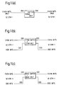
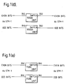
- Switch Units For a range of switches, from 32 STM-1 interfaces of 155.52 Mbit/s, up to 320 STM-1 interfaces, 4 configurations can be used.
- 1 Switch Unit for 32 STM-1 interfaces 2 Switch Units for 64 STM-1 interfaces 5 Switch Units for 160 STM-1 interfaces 10 Switch Units for 320 STM-1 interfaces
- Figure 1 gives some examples 1(a) 32 STM-1s 1 Switch Unit 155520 channels of 32 kbit/s 1(b) 32 STM-1s 1 Switch Unit 77760 channels of 64 kbit/s 1(c) 32 STM-1s 1 Switch Unit 8640 columns for VC switching 1(d) 64 STM-1s 2 Switch Units 155520 channels of 64 kbit/s 1(e) 64 STM-1s 2 Switch Units 17280 columns for VC switching 1(f) 128 STM-1s 5 Switch Units 43200 columns for VC switching 1(g) 320 STM-1s 10 Switch Units 86400 columns for VC switching Bit Spreading units are
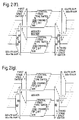
- the same switch unit is used for all the above 7 arrangements. It has to operate in 6 different modes to achieve the required switching granularity. The same mode is used for both the 1(a) and 1(d) arrangement.
- Figure 2(a) to 2(g) gives the 6 arrangements, of the Space-Time-Spacing switching structure that are used. It receives 64 cables of 116.64 Mbit/s carrying the odd or even bits of an STM-1, or individual bit numbers of 5 different STM-1s. Consequently a single switching unit can handle the equivalent of 32 STM-1s.
- All the switching IC inputs and outputs run at a data rate of 19.44 Mbit/s, while the connections through the backplane are at 116.64 Mbit/s.
- the time switch elements and time multiplexed space switch elements can operate with; 486 channels of 5 bits over a switching frame of 125 ⁇ s or 45 channels of 5 bits over a switching frame of 13.9 ⁇ s or 270 channels of 1 bit over a switching frame of 13.9 ⁇ s 13.9 is is one ninth of 125 ⁇ s and corresponds to an SDH row, as described earlier.
- time switching element Because the time switching element has 8 inputs and 8 outputs it handles 8 times these numbers of channels namely, 3888, 432 and 2160 channels for the above 3 arrangements.
- the space switch elements supply the CLOS fanout and are either; 40 x 80 and 80 x 40 or dual 20 x 40 and 40 x 20
- arrangements 2(c), 2(e), 2(f) and 2(g) do not offer 64 kbit/s switching. Therefore path set ups are performed with a granularity of a column and a switching frame of a row. Whereas for arrangements 2(b) and 2(d), path set ups are performed with a granularity of 64 kbit/s. Arrangements 2(b) and 2(d) can perform VC switching, so 64 kbit/s and VC switching can be performed on the same switch, up to a maximum of 64 STM-1 or equivalent interfaces.
- Arrangement 2(a) uses the same configuration of the switching unit as 2(d), but with only one of the switching units.
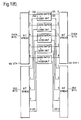
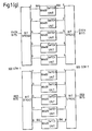
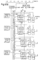
- a Switching Unit contains a 3 stage Space-Time-Space function. There are 8 Outer Space Switching cards. Each Outer Space Switch card carries one first stage space switching element and one third stage space switching element. There are also 8 Central Time Switching cards. Each Central Time Switching card carries 10 second stage time switching elements.
- Bit spreading occurs on these small VC switches as byte wide data is naturally bit spread.
- a switching element is a functionnal part of the switching architecture, there is no necessity that a switching element is a single integrated circuit.
- the architecture is such that the switching elements can be built from Application Specific Integrated Circuits (ASICs) which are of a reasonable size, without large numbers of outputs, without high speed I/Os, without large packages, and without high power dissipation.
- ASICs Application Specific Integrated Circuits
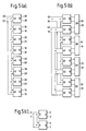
- the time-multiplexed space switch ASIC has 40 input switching inputs and 10 outputs. 8 such ASICs can be configured as a 40 x 80 space switch element as shown in Figure 5(a). 8 such ASICs can also be configured as an 80 x 40 space switch element, as shown in Figure 5(b).
- the time switch ASIC has 8 switching inputs and 4 switching outputs. 2 of these ASICs are required to make an 8 x 8 time switching element, as shown in Figure 5(c).
- the Space Switching ASIC has a 40 to 1 multiplexer and a Control Store. There is also a single serial control interface function.
- Each Location of the control store contains 6 bits. 6 bits is sufficient to define which of the 40 inputs is required with some spare values to define what to output when no input is selected. This is essential for idle and diagnostic patterns.
- control store needs 486 locations. Therefore the total control store RAM of the 40 x 10 Space Switching ASIC requires 29160 bits.
- the ASIC contains; Control Store RAMs, Serial In/parallel Out Registers, a Barrel Shifter, Speech (traffic) Store RAMs and one serial control interface function.
- Figure 6(a) shows the general arrangement of the switching ASIC for 5 bit switching and Figure 6(b) for 1 bit switching.
- a control store is also needed for each output of the Time Switching ASIC and each needs 486 locations. Because there are a maximum of 3888 channels entering the ASIC, at least 12 bits are needed to select an input channel. 13 bits are provided to supply enough spare values to define what to output when no input is selected.
- the 4 control store RAMs therefore need to each be 486 x 13, giving a total of 25272 bits.
- control store does not contain an absolute address of a speech store location. When a speech store access is to be made, the control store is still read. However, it indicates how many memory write cycles have occurred since the require input data was written into the speech store. As the last location written to the speech store is known, the required speech store address can be computed.
- the depth of the speech store only needs to correspond to the maximum duration for which any data needs to reside in the speech store.
- the Speech Store memory requirement when considering the 64 kbit/s switching needs, has to be able to handle 4096 channels of 5 bits.
- 4096 channels is 512 x 8, as opposed to 486 x 8 which is 3888.
- the Memory therefore has to be organised so that the 8 writes can be performed in parallel during one clock cycle, leaving the other 4 clocks for the 4 random read accesses.
- the actual arrangement chosen is 8 RAM blocks of 128 by 20, with a 32:1 selector implemented in two major stages.
- the multiplexors used also contain further circuitry for injecting idle and test patterns under direction from the control store, although the connections for these are not shown in the Figures.
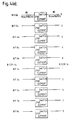
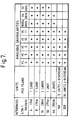
- the table shown in Figure 7 lists possible growth states. It also defines the minimum granularity that can be handled by each growth state and indicates the quantity of switching hardware per security plane.
- the example is for a single stage time switch.
- Switch Format 2 carries 9 times the bandwidth of Switch Format 1.
- the number of inputs is the same (I) (Also equal to the number of inputs).
- the number of input channels is the same (C) (Also equal to the number of output channels).
- the data rate per input is the same (C x 9 bits per Frame).
- the size of the control store is the same:- Locations, one per output channel, (I x C) Bits per location is n (where 2 to the power n is greater than I x C)
- the size of the speech/traffic store control - Minimum number of Locations; one per input channel (I x C) Bits per location; Switch Format 1 9 bits Switch Format 2 1 bit Read Access Rate; Switch Format 1 every 9 bits Switch Format 2 every bit
- Switch Formats 1 and 2 The organisation of the memory is different for Switch Formats 1 and 2 but provided it is constructed of several suitable blocks it can be used for either Switch function. When the number of Inputs (I) also equals 9 then it becomes quite straight forward with the addition of suitable multiplexors.
Landscapes
- Engineering & Computer Science (AREA)
- Computer Networks & Wireless Communication (AREA)
- Use Of Switch Circuits For Exchanges And Methods Of Control Of Multiplex Exchanges (AREA)
- Time-Division Multiplex Systems (AREA)
Applications Claiming Priority (2)
| Application Number | Priority Date | Filing Date | Title |
|---|---|---|---|
| GB929204100A GB9204100D0 (en) | 1992-02-26 | 1992-02-26 | Reconfigurable switch memory |
| GB9204100 | 1992-02-26 |
Publications (2)
| Publication Number | Publication Date |
|---|---|
| EP0558291A2 true EP0558291A2 (de) | 1993-09-01 |
| EP0558291A3 EP0558291A3 (en) | 1995-02-15 |
Family
ID=10711083
Family Applications (1)
| Application Number | Title | Priority Date | Filing Date |
|---|---|---|---|
| EP93301358A Withdrawn EP0558291A3 (en) | 1992-02-26 | 1993-02-24 | Reconfigurable switch memory |
Country Status (4)
| Country | Link |
|---|---|
| US (1) | US5504739A (de) |
| EP (1) | EP0558291A3 (de) |
| JP (1) | JPH0646469A (de) |
| GB (2) | GB9204100D0 (de) |
Cited By (4)
| Publication number | Priority date | Publication date | Assignee | Title |
|---|---|---|---|---|
| DE19961132C1 (de) * | 1999-12-17 | 2001-06-28 | Siemens Ag | Zeit- /Raumkoppelbaustein mit Mehrfachfunktionalität |
| US6366579B1 (en) | 1997-08-28 | 2002-04-02 | Telefonaktiebolaget Lm Ericsson (Publ) | Modular time-space switch |
| EP1087637A3 (de) * | 1999-09-27 | 2003-01-02 | Nortel Networks Limited | Kompakter Schalter mit hoher Kapazität |
| CN100361103C (zh) * | 2005-06-22 | 2008-01-09 | 钰创科技股份有限公司 | 液晶电视系统的可模块化配置的内存系统 |
Families Citing this family (7)
| Publication number | Priority date | Publication date | Assignee | Title |
|---|---|---|---|---|
| GB9405993D0 (en) * | 1994-03-25 | 1994-05-11 | Plessey Telecomm | Multipurpose synchronous switch architecture |
| US6459788B1 (en) * | 1999-04-27 | 2002-10-01 | Sprint Communications Company L.P. | Call center resource processor |
| KR100332410B1 (ko) * | 1999-09-28 | 2002-04-13 | 서평원 | 유사 클로즈 네트워크에서의 가상컨테이너 신호들의 복합경로 탐색방법 |
| US7184662B2 (en) * | 2001-10-10 | 2007-02-27 | Bay Microsysems, Inc. | Switching network |
| JP5307900B2 (ja) | 2008-11-17 | 2013-10-02 | べシックス・バスキュラー・インコーポレイテッド | 組織トポグラフィの知識によらないエネルギーの選択的な蓄積 |
| US8369321B2 (en) * | 2010-04-01 | 2013-02-05 | Juniper Networks, Inc. | Apparatus and methods related to the packaging and cabling infrastructure of a distributed switch fabric |
| CN102014060B (zh) * | 2010-11-25 | 2012-12-19 | 华为技术有限公司 | 时间透传转码ttt传送的报文发送和获取的方法以及发送和接收设备 |
Family Cites Families (6)
| Publication number | Priority date | Publication date | Assignee | Title |
|---|---|---|---|---|
| FR2127392A5 (de) * | 1971-03-05 | 1972-10-13 | Constr Telephoniques | |
| GB1573807A (en) * | 1978-04-03 | 1980-08-28 | Gen Electric Co Ltd | Digital telecommunication exchange |
| US4704716A (en) * | 1985-12-31 | 1987-11-03 | American Telephone And Telegraph Company, At&T Bell Laboratories | Method and apparatus for establishing a wideband communication facility through a communication network having narrow bandwidth channels |
| US4998242A (en) * | 1988-12-09 | 1991-03-05 | Transwitch Corp. | Virtual tributary cross connect switch and switch network utilizing the same |
| US4965787A (en) * | 1989-02-09 | 1990-10-23 | Data General Corporation | Methods and apparatus for multiplexing sub-rate channels in a digital data communication system |
| GB9105922D0 (en) * | 1991-03-20 | 1991-05-08 | Plessey Telecomm | Time switch speech store module |
-
1992
- 1992-02-26 GB GB929204100A patent/GB9204100D0/en active Pending
-
1993
- 1993-02-24 EP EP93301358A patent/EP0558291A3/en not_active Withdrawn
- 1993-02-24 GB GB9303711A patent/GB2264612B/en not_active Expired - Fee Related
- 1993-02-26 JP JP5062619A patent/JPH0646469A/ja active Pending
-
1994
- 1994-09-20 US US08/309,562 patent/US5504739A/en not_active Expired - Fee Related
Cited By (6)
| Publication number | Priority date | Publication date | Assignee | Title |
|---|---|---|---|---|
| US6366579B1 (en) | 1997-08-28 | 2002-04-02 | Telefonaktiebolaget Lm Ericsson (Publ) | Modular time-space switch |
| EP1087637A3 (de) * | 1999-09-27 | 2003-01-02 | Nortel Networks Limited | Kompakter Schalter mit hoher Kapazität |
| US6704307B1 (en) | 1999-09-27 | 2004-03-09 | Nortel Networks Limited | Compact high-capacity switch |
| DE19961132C1 (de) * | 1999-12-17 | 2001-06-28 | Siemens Ag | Zeit- /Raumkoppelbaustein mit Mehrfachfunktionalität |
| US6885663B2 (en) | 1999-12-17 | 2005-04-26 | Siemens Aktiengesellschaft | Time/space switching component with multiple functionality |
| CN100361103C (zh) * | 2005-06-22 | 2008-01-09 | 钰创科技股份有限公司 | 液晶电视系统的可模块化配置的内存系统 |
Also Published As
| Publication number | Publication date |
|---|---|
| US5504739A (en) | 1996-04-02 |
| GB2264612B (en) | 1996-01-17 |
| GB9204100D0 (en) | 1992-04-08 |
| JPH0646469A (ja) | 1994-02-18 |
| GB9303711D0 (en) | 1993-04-14 |
| GB2264612A (en) | 1993-09-01 |
| EP0558291A3 (en) | 1995-02-15 |
Similar Documents
| Publication | Publication Date | Title |
|---|---|---|
| US4725835A (en) | Time multiplexed bus matrix switching system | |
| US5430687A (en) | Programmable logic device including a parallel input device for loading memory cells | |
| JP2931189B2 (ja) | 交換接続の設立方法及び装置 | |
| US5504739A (en) | Reconfigurable switch memory | |
| JP2928070B2 (ja) | 接続交換装置及びその制御方法 | |
| JP2931188B2 (ja) | データレート切り換え用交換素子及び切り換え方法 | |
| US5809032A (en) | Time division multiplexed synchronous state machine having state memory | |
| CA2445001C (en) | Architectures for a single-stage grooming switch | |
| JP2944868B2 (ja) | 交換配置及び交換方法 | |
| EP0506134B1 (de) | ATM-Zellenmultiplexeinrichtung zur Reduzierung der Zugriffsgeschwindigkeit für einen FIFO-Speicher | |
| US6584121B1 (en) | Switch architecture for digital multiplexed signals | |
| US4686670A (en) | Method of switching time slots in a TDM-signal and arrangement for performing the method | |
| CA2049478C (en) | Atm switch circuit configuration system | |
| US5177742A (en) | Demultiplexer for a serial and isochronous multiplex signal | |
| KR0144326B1 (ko) | 12*12 에스티에스-1 스위치 | |
| US20050071594A1 (en) | Memory partitioning | |
| EP0256297A2 (de) | Bit-Koppelpunktschalter | |
| US7315540B2 (en) | Random access memory based space time switch architecture | |
| US5822316A (en) | ATM switch address generating circuit | |
| EP1585272B1 (de) | Schaltmatrix für ein Telekommunikationsnetzwerkelement | |
| US6948030B1 (en) | FIFO memory system and method | |
| KR100378588B1 (ko) | 대용량화가 가능한 다중 경로 비동기 전송 모드 스위치 및 셀구조 | |
| BR9811378B1 (pt) | estrutura de comutação modular para dados de comutação de circuito, e, comutador de comunicação modular para comutar o circuito de dados. | |
| EP1565032B1 (de) | Niedrige Redundanzdatenramarchitektur für monolithische Zeit-/Raumvermittlungsschalter | |
| US7978736B2 (en) | Efficient provisioning of a VT/TU cross-connect |
Legal Events
| Date | Code | Title | Description |
|---|---|---|---|
| PUAI | Public reference made under article 153(3) epc to a published international application that has entered the european phase |
Free format text: ORIGINAL CODE: 0009012 |
|
| AK | Designated contracting states |
Kind code of ref document: A2 Designated state(s): DE ES FR IT SE |
|
| PUAL | Search report despatched |
Free format text: ORIGINAL CODE: 0009013 |
|
| AK | Designated contracting states |
Kind code of ref document: A3 Designated state(s): DE ES FR IT SE |
|
| 17P | Request for examination filed |
Effective date: 19950502 |
|
| RAP1 | Party data changed (applicant data changed or rights of an application transferred) |
Owner name: MARCONI COMMUNICATIONS LIMITED |
|
| 17Q | First examination report despatched |
Effective date: 20000214 |
|
| STAA | Information on the status of an ep patent application or granted ep patent |
Free format text: STATUS: THE APPLICATION IS DEEMED TO BE WITHDRAWN |
|
| 18D | Application deemed to be withdrawn |
Effective date: 20000627 |