EP0559996B1 - Circuit de commande, en particulier pour demi-ponts à MOS de puissance - Google Patents
Circuit de commande, en particulier pour demi-ponts à MOS de puissance Download PDFInfo
- Publication number
- EP0559996B1 EP0559996B1 EP92830119A EP92830119A EP0559996B1 EP 0559996 B1 EP0559996 B1 EP 0559996B1 EP 92830119 A EP92830119 A EP 92830119A EP 92830119 A EP92830119 A EP 92830119A EP 0559996 B1 EP0559996 B1 EP 0559996B1
- Authority
- EP
- European Patent Office
- Prior art keywords
- circuit
- output
- voltage
- reference potential
- fact
- Prior art date
- Legal status (The legal status is an assumption and is not a legal conclusion. Google has not performed a legal analysis and makes no representation as to the accuracy of the status listed.)
- Expired - Lifetime
Links
Images

Classifications
-
- H—ELECTRICITY
- H03—ELECTRONIC CIRCUITRY
- H03K—PULSE TECHNIQUE
- H03K17/00—Electronic switching or gating, i.e. not by contact-making and –breaking
- H03K17/06—Modifications for ensuring a fully conducting state
- H03K17/063—Modifications for ensuring a fully conducting state in field-effect transistor switches
-
- H—ELECTRICITY
- H03—ELECTRONIC CIRCUITRY
- H03K—PULSE TECHNIQUE
- H03K17/00—Electronic switching or gating, i.e. not by contact-making and –breaking
- H03K17/51—Electronic switching or gating, i.e. not by contact-making and –breaking characterised by the components used
- H03K17/56—Electronic switching or gating, i.e. not by contact-making and –breaking characterised by the components used by the use, as active elements, of semiconductor devices
- H03K17/687—Electronic switching or gating, i.e. not by contact-making and –breaking characterised by the components used by the use, as active elements, of semiconductor devices the devices being field-effect transistors
- H03K17/6871—Electronic switching or gating, i.e. not by contact-making and –breaking characterised by the components used by the use, as active elements, of semiconductor devices the devices being field-effect transistors the output circuit comprising more than one controlled field-effect transistor
-
- H—ELECTRICITY
- H03—ELECTRONIC CIRCUITRY
- H03K—PULSE TECHNIQUE
- H03K17/00—Electronic switching or gating, i.e. not by contact-making and –breaking
- H03K17/51—Electronic switching or gating, i.e. not by contact-making and –breaking characterised by the components used
- H03K17/56—Electronic switching or gating, i.e. not by contact-making and –breaking characterised by the components used by the use, as active elements, of semiconductor devices
- H03K17/687—Electronic switching or gating, i.e. not by contact-making and –breaking characterised by the components used by the use, as active elements, of semiconductor devices the devices being field-effect transistors
- H03K17/6877—Electronic switching or gating, i.e. not by contact-making and –breaking characterised by the components used by the use, as active elements, of semiconductor devices the devices being field-effect transistors the control circuit comprising active elements different from those used in the output circuit
Definitions
- the present invention relates to a drive circuit, particularly for power MOS half-bridges.
- Power MOS half-bridges comprise a pair of power MOS transistors, usually N-channel type, push-pull connected as shown by way of example in Fig.1, which shows a half-bridge 1 comprising two MOS (typically VDMOS-Vertical Double Diffused MOS) transistors M 1 and M 2 .
- Transistor M 1 top transistor presents its drain terminal connected to supply voltage V S , and its source terminal connected to the drain terminal of transistor M 2 (bottom transistor), the source terminal of which is grounded.
- the gate terminals of transistors M 1 and M 2 are connected respectively to top and bottom drivers T and B in turn connected to a synchronizing input signal IN, for producing drive signals whereby one of transistors M 1 , M 2 is turned off when the other is on.
- the output of half-bridge 1 thus presents a signal V OUT , the amplitude of which switches between R DSon2 ⁇ I (where R DSon2 is the equivalent resistance between the drain and source of transistor M 2 when saturated, and I the output current) and V S - R DSOn1 ⁇ I (where R DSON1 is the equivalent resistance between the drain and source of transistor M 1 when saturated).
- V GS gate-source voltage
- Such a high voltage is usually achieved without difficulty as regards transistor M 2 , which permits the use of a reference voltage obtainable from the supply voltage.
- the situation is more complex, however, in the case of transistor M 1 , which requires a drive voltage of 10V + V OUT , i.e. 10V + V S - R DSon1 ⁇ I, which is higher than the supply voltage.
- a highly effective solution to the problem is to use a charge-pump or voltage doubling circuit, which gives a voltage higher than the supply voltage, and provides for driving one or more half-bridges.
- a simplified diagram of such a circuit, indicated by 2 is shown in Fig.2.
- Charge-pump circuit 2 substantially comprises an oscillator 3; two condensers 4 and 5; and two diodes 6 and 7.
- Oscillator 3 is connected to a reference voltage V REF and ground, so that its output 8 switches continually between V REF and 0V.
- condenser 4 charges to V S via diode 6; whereas, in the second half-cycle, when output 8 equals V REF , condenser 4 (whose terminal 9, not connected to oscillator 3, switches to voltage V REF + V S in relation to ground) transfers the charge to condenser 5.
- diode 6 disconnects condensers 4 and 5 from supply V S , while, in the first half-cycle, in which condenser 4 restores the charge transferred to condenser 5, diode 7 disconnects condenser 5 from condenser 4 and the supply voltage.
- Charge-pump circuit 2 therefore provides a drive voltage ensuring a sufficient voltage drop V GS in transistor M 1 to effectively saturate it.
- Reference voltage V REF is usually produced using circuit 10 in Fig.3, which presents a minimum voltage difference D V between supply and reference voltages V S and V REF .
- Circuit 10 comprises a bipolar NPN transistor 11; a resistor 12 connected between the base and collector of transistor 11; and two diodes 13, 14, of which diode 13 is a Zener, connected in series between the base of transistor 11 and ground.
- the emitter of transistor 11 is connected to supply voltage V S , and the base defines the output of circuit 10.
- Fig.3 circuit is impractical, as in the case of automotive applications, which require that the MOS half-bridge, operating normally with a supply voltage V S of 6V, should also be capable of operating with a minimum supply voltage V Smin of 5.4V, i.e. that the drive circuit of top transistor M 1 supply an output voltage V CP of at least roughly 9.3V.
- VDMOS transistors must be driven in such a manner as to present a voltage drop V GS of at least 4V. This is obtained easily, in the case of transistor M 2 , even with a minimum supply voltage V Smin . The same does not apply, however, to transistor M 1 , which, with a minimum supply voltage V Smin of 5.4V, requires that V OUT ⁇ 5.3V and, therefore, V CP ⁇ 9.3V.
- V REF reference voltage
- PNP transistor 15 presents an emitter connected to supply voltage V S , and a collector defining the output of the circuit.
- a resistor 16 is connected parallel to the base-emitter junction of transistor 15; a current source 17 is connected between the base of transistor 15 and ground; and a Zener diode 18 is also connected between the output and ground.
- MOS half-bridge drive circuit particularly for power MOS half-bridges, as claimed in Claim 1.
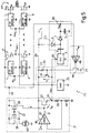
- Drive circuit 20 in Fig.5 substantially comprises a linear voltage regulator 21; a firing circuit 22; a charge-pump circuit 23; a comparator stage 24; a load 25; a first group of bottom drivers B; and a second group of top drivers T.
- Linear voltage regulator 21 (defining a voltage source) comprises an operational amplifier 30, the output 31 of which is connected to the gate terminal of a preferably VDMOS transistor 32, the drain terminal of which is connected to supply line 29 (reference potential line on which voltage V S is present), and the source terminal of which is grounded via two series connected feedback resistors 33, 34.
- the mid point between the source terminal of transistor 32 and resistor 33 defines output 35 of regulator 21 at which reference voltage V REF is present; while the mid point between feedback resistors 33, 34 is connected to the inverting terminal of operational amplifier 30.
- the non-inverting terminal of amplifier 30 receives a precise, temperature-stable voltage V bg produced, for example, by a so-called band-gap circuit.
- Operational amplifier 30 also presents a supply input 36 connected to supply line 29.
- Regulator 21 also comprises a current mirror circuit 37 comprising two P-channel MOS transistors 38, 39.
- the gate and drain terminals of transistor 38 are shortcircuited and connected to a current source 40; while the drain terminal of transistor 39 is connected to output 31 of operational amplifier 30.
- the source terminals of both transistors 38, 39 are connected to output 42 of charge-pump circuit 23 over line 43.
- Firing circuit 22 comprises a bipolar NPN transistor 44 with its collector connected directly to supply line 29, the base connected to supply line 29 via a resistor 45, and the emitter connected to output 35 of regulator 21 and to input 46 of oscillator 3 of charge-pump circuit 23.
- circuit 23 (which forms a voltage elevating circuit) also comprises a condenser 4 having one terminal connected to the output of oscillator 3, and the other terminal connected to the cathode of diode 6, the anode of which is connected to supply line 29.
- the cathode of diode 6 is also connected to the anode of diode 7, the cathode of which defines output 42 to which drive voltage V CP is supplied.
- Condenser 5 is located between output 42 and ground.
- Comparator stage 24 (defining switch means for turning off firing circuit 22) in turn comprises a comparator 48, the non-inverting input of which is connected to output 42 of charge-pump circuit 23, and the inverting input of which receives reference voltage V TR .
- the output of comparator 48 is connected to the gate terminal of a MOS transistor 49, the source terminal of which is grounded, and the drain terminal of which is connected to the base of transistor 44 of firing circuit 22.
- Load 25 and bottom drivers B are connected to output 35 of regulator 21, while top drivers T are connected to output 42 of charge-pump circuit 23.
- Bottom drivers B for driving respective bottom transistors M 2.1 -M 2.N of half-bridges 1.1-1.N by switching them according to the operating frequency of the half-bridges, receive respective synchronizing input signals IN.1-IN.N, which are also supplied to respective top drivers T for driving top transistors M 1.1 -M 1.N of the same half-bridges 1.1-1.N in the same way as, but in phase opposition to drivers B, and with a higher voltage, as already described.
- Top and bottom drivers T and B are also grounded, while the respective half-bridges 1.1-1.N present outputs OUT1-OUTN.
- the Fig.5 drive circuit operates as follows.
- V CP is supplied to current mirror circuit 37, which therefore drives transistor 32 by bringing its gate terminal up to voltage V CP .
- V S and V REF Prior to reaching the normal operating condition, the reduction in the difference between V S and V REF is also accompanied by a reduction in the voltage drop at the base-emitter junction of transistor 44 of firing circuit 22, until transistor 44 eventually goes off.
- top and bottom drivers T and B function correctly, by virtue of the gate-source junction being supplied with a voltage V GS of at least 4V.
- Firing circuit 22 is also turned off by comparator stage 24, especially in the presence of a high supply voltage V S (which may be as high as 60V), and, in particular, when the output voltage V CP of charge-pump circuit 23 is such as to ensure the system is turned on, and prior to output voltage V REF of regulator 21 reaching the normal operating value.
- V S which may be as high as 60V
- V CP exceeds voltage V TR at the inverting input of comparator 48
- the output of comparator 48 switches from low to high, thus turning on transistor 49, and the voltage at the drain terminal of transistor 49 becomes low, thus inversely biasing the base-emitter junction of transistor 44.
- a further advantage of actively turning off firing circuit 22 (by connecting the base terminal of transistor 44 to a voltage close to 0 V) is that it enables transistor 44 to withstand breakdown voltage BV CBO .
- the circuit according to the present invention also provides for generating an optimum reference voltage, e.g. of 10 V, as required for driving MOS half-bridges in the best possible manner.
- the circuit is also straightforward in design, and easily implementable, for example, as an integrated circuit.
- firing circuit 22 may be insufficient for supplying the current required, it may be replaced by circuit 22' as shown in Fig.6.
- circuit 22' features two transistors: a PNP transistor 53 with its emitter terminal connected to supply line 29, its base terminal connected to one terminal of resistor 45 and to the drain terminal of transistor 49 of comparator stage 24, and its collector terminal connected to the base terminal of a second NPN transistor 54, the collector terminal of which is connected to supply line 29, and the emitter terminal to output 35 of regulator 21. Finally, a current source 55, supplying current I 1 , is provided between the base terminal of transistor 53 and ground.
Landscapes
- Dc-Dc Converters (AREA)
- Control Of Electrical Variables (AREA)
- Power Conversion In General (AREA)
- Amplifiers (AREA)
- Electronic Switches (AREA)
Claims (14)
- Circuit d'attaque (20) pour demi-ponts MOS (1), en particulier pour des demi-ponts MOS de puissance, comprenant une première ligne de potentiel de référence (29) présentant un premier potentiel de référence (VS); un circuit générateur de tension (21) comportant une entrée (36) connectée à ladite première ligne de potentiel de référence (29) et une sortie (35) délivrant un deuxième potentiel de référence (VREF); et un circuit élévateur de tension (23) présentant une première et une seconde entrée (46) connectées respectivement à ladite première ligne de potentiel de référence (29) et à ladite sortie (35) dudit circuit générateur de tension (21); ledit circuit élévateur de tension (23) présentant aussi une sortie (42) délivrant, sous des conditions de fonctionnement normal, un potentiel d'attaque (VCP) supérieur audit premier potentiel de référence (VS) et augmentant avec ledit deuxième potentiel de référence (VREF); caractérisé en ce que ledit circuit générateur de tension (21) présente une autre entrée connectée à ladite sortie (42) dudit circuit élévateur de tension (23), et comprend un moyen de contre-réaction positive (37, 43) connecté à ladite autre entrée afin d'augmenter, en présence d'un premier potentiel de référence faible, ledit deuxième potentiel de référence (VREF) à une valeur maximum de fonctionnement normal simultanément à une augmentation dudit potentiel d'attaque (VCP).
- Circuit selon la revendication 1, caractérisé en ce que ledit circuit générateur de tension (21) comprend un régulateur de tension (30 à 34) présentant une entrée connectée à ladite sortie (42) dudit circuit élévateur de tension (23) par l'intermédiaire dudit moyen de contre-réaction positive.
- Circuit selon la revendication 2, caractérisé en ce que ledit régulateur de tension (30 à 34) comprend un moyen formant transistor de sortie (32) présentant une borne de commande connectée par l'intermédiaire dudit moyen de contre-réaction positive à ladite sortie (42) dudit circuit élévateur de tension (23), et une borne de sortie définissant ladite sortie (35) dudit circuit générateur de tension (21).
- Circuit selon la revendication 3, caractérisé en ce que ledit moyen formant transistor de sortie comprend un transistor MOS (32) présentant une borne de grille connectée par l'intermédiaire dudit moyen de contre-réaction à ladite sortie (42) dudit circuit élévateur de tension (23), une borne de source définissant ladite borne de sortie (35), et une borne de drain connectée à ladite première ligne de potentiel de référence (29).
- Circuit selon la revendication 3 ou 4, caractérisé en ce que ledit régulateur de tension (30 à 34) comprend un amplificateur opérationnel (30) présentant une entrée positive connectée à un troisième potentiel de référence (Vbg), une entrée négative connectée à ladite borne de sortie (35) dudit circuit générateur de tension par l'intermédiaire d'un circuit de contre-réaction résistif (33, 34) connecté aussi à une quatrième ligne de potentiel de référence (masse), et une sortie (31) connectée à ladite borne de commande dudit moyen formant transistor de sortie (32).
- Circuit selon l'une quelconque des revendications 2 à 5 précédentes, caractérisé en ce qu'un circuit miroir de courant (37) est prévu pour ledit moyen de contre-réaction positive, entre ladite sortie (35) dudit circuit générateur de tension (21) et ladite sortie (42) dudit circuit élévateur de tension (23).
- Circuit selon l'une quelconque des revendications 1 à 6 précédentes, caractérisé en ce qu'il comprend un circuit de déclenchement (22; 22') entre ladite première ligne de potentiel de référence (29) et ladite seconde entrée (46) dudit circuit élévateur de tension (23).
- Circuit selon la revendication 7, caractérisé en ce que ledit circuit de déclenchement (22; 22') comprend un moyen formant transistor (44; 53, 54) présentant une première borne connectée à ladite première ligne de potentiel de référence (29), une deuxième borne de commande connectée à ladite première ligne de potentiel de référence par l'intermédiaire d'un moyen résistif (45), et une troisième borne connectée à ladite seconde entrée (46) dudit circuit élévateur de tension (23).
- Circuit selon la revendication 8, caractérisé en ce que ledit moyen formant transistor comprend un transistor bipolaire (44).
- Circuit selon la revendication 8, caractérisé en ce que ledit moyen formant transistor comprend deux transistors bipolaires connectés en cascade (53, 54).
- Circuit selon l'une quelconque des revendications 7 à 9 précédentes, caractérisé en ce qu'il comprend un moyen de commutation (24) connecté à une borne de commande dudit circuit de déclenchement (22; 22'), afin de désactiver ledit circuit de déclenchement avant que ledit circuit d'attaque (20) n'atteigne des conditions de fonctionnement normal.
- Circuit selon la revendication 11, caractérisé en ce que ledit moyen de commutation comprend un étage comparateur (24) présentant une première entrée connectée à ladite sortie (42) dudit circuit élévateur de tension (23), une deuxième entrée connectée à un potentiel de seuil (VTR) et une sortie connectée à ladite borne de commande dudit circuit de déclenchement (22; 22').
- Circuit selon l'une quelconque des revendications précédentes, caractérisé en ce que ledit circuit élévateur de tension (23) comprend un circuit à pompage de charge.
- Circuit selon la revendication 13, caractérisé en ce que ledit circuit à pompage de charge (23) comprend un étage oscillateur (3) présentant une entrée (46) connectée à ladite sortie (35) dudit circuit générateur de tension (21), et une sortie connectée à une première borne d'un premier condensateur (4) présentant une seconde borne connectée à ladite première ligne de potentiel de référence (29) par l'intermédiaire d'une première diode (6) et à ladite sortie (42) dudit circuit élévateur de tension (23) par l'intermédiaire d'une seconde diode (7); un second condensateur (5) étant prévu entre ladite sortie (42) dudit circuit élévateur de tension (23) et une quatrième ligne de potentiel de référence (masse).
Priority Applications (5)
| Application Number | Priority Date | Filing Date | Title |
|---|---|---|---|
| EP92830119A EP0559996B1 (fr) | 1992-03-12 | 1992-03-12 | Circuit de commande, en particulier pour demi-ponts à MOS de puissance |
| DE69222144T DE69222144T2 (de) | 1992-03-12 | 1992-03-12 | Treiber, insbesondere für Leistungs-MOS-Halbbrücken |
| US08/029,691 US5376832A (en) | 1992-03-12 | 1993-03-11 | MOS half-bridge drive circuit, particularly for power MOS half-bridges |
| JP5052482A JPH0698529A (ja) | 1992-03-12 | 1993-03-12 | Mos半ブリッジの駆動回路 |
| US08/318,350 US5541540A (en) | 1992-03-12 | 1994-10-05 | MOS half-bridge drive circuit, particularly for power MOS half-bridges |
Applications Claiming Priority (1)
| Application Number | Priority Date | Filing Date | Title |
|---|---|---|---|
| EP92830119A EP0559996B1 (fr) | 1992-03-12 | 1992-03-12 | Circuit de commande, en particulier pour demi-ponts à MOS de puissance |
Publications (2)
| Publication Number | Publication Date |
|---|---|
| EP0559996A1 EP0559996A1 (fr) | 1993-09-15 |
| EP0559996B1 true EP0559996B1 (fr) | 1997-09-10 |
Family
ID=8212079
Family Applications (1)
| Application Number | Title | Priority Date | Filing Date |
|---|---|---|---|
| EP92830119A Expired - Lifetime EP0559996B1 (fr) | 1992-03-12 | 1992-03-12 | Circuit de commande, en particulier pour demi-ponts à MOS de puissance |
Country Status (4)
| Country | Link |
|---|---|
| US (2) | US5376832A (fr) |
| EP (1) | EP0559996B1 (fr) |
| JP (1) | JPH0698529A (fr) |
| DE (1) | DE69222144T2 (fr) |
Families Citing this family (20)
| Publication number | Priority date | Publication date | Assignee | Title |
|---|---|---|---|---|
| US6407594B1 (en) | 1993-04-09 | 2002-06-18 | Sgs-Thomson Microelectronics S.R.L. | Zero bias current driver control circuit |
| EP0675584B1 (fr) * | 1994-03-29 | 1999-01-13 | STMicroelectronics S.r.l. | Etage de sortie de puissance avec absorption de courant limitée pendant la phase de haute impédance |
| JPH0897706A (ja) * | 1994-09-26 | 1996-04-12 | Nec Corp | 出力バッファ回路 |
| GB9423046D0 (en) * | 1994-11-15 | 1995-01-04 | Sgs Thomson Microelectronics | A voltage reference circuit |
| US5796276A (en) * | 1994-12-30 | 1998-08-18 | Sgs-Thomson Microelectronics, Inc. | High-side-driver gate drive circuit |
| US5740109A (en) * | 1996-08-23 | 1998-04-14 | Motorola, Inc. | Non-linear charge pump |
| DE69841763D1 (de) * | 1997-10-28 | 2010-08-26 | Nxp Bv | Halbleiterbauelement mit einem halbbrücken-schaltkreis |
| US6477079B2 (en) | 1999-05-18 | 2002-11-05 | Kabushiki Kaisha Toshiba | Voltage generator for semiconductor device |
| US6140805A (en) * | 1999-05-18 | 2000-10-31 | Kabushiki Kaisha Toshiba | Source follower NMOS voltage regulator with PMOS switching element |
| GB2404507B (en) * | 2003-07-31 | 2006-06-21 | Zetex Plc | A high side switching circuit |
| JP4820544B2 (ja) * | 2004-10-27 | 2011-11-24 | 株式会社エヌエフ回路設計ブロック | リニア動作の電力増幅回路および電力増幅器 |
| DE202006005725U1 (de) * | 2006-04-07 | 2007-08-16 | Wyremba, Hans-Peter | Treiberanordnung für ein Gate zumindest eines Transistors |
| CN101135718B (zh) * | 2007-09-10 | 2010-06-02 | 中兴通讯股份有限公司 | 一种驱动器电路 |
| US8222927B2 (en) * | 2009-04-09 | 2012-07-17 | Mediatek Inc. | Reference buffer circuit |
| JP2012060550A (ja) * | 2010-09-13 | 2012-03-22 | Mitsubishi Electric Corp | 電力増幅器 |
| CN103516340B (zh) * | 2012-06-29 | 2017-01-25 | 快捷半导体(苏州)有限公司 | 一种最大电压选择电路、方法及子选择电路 |
| TWI495246B (zh) * | 2012-10-24 | 2015-08-01 | Nat Univ Tsing Hua | 諧振直流轉換器 |
| EP3193436B1 (fr) * | 2016-01-15 | 2019-10-30 | Nxp B.V. | Circuit de pompe de charge pour controler un interrupteur de connexion de charge |
| US11942929B2 (en) * | 2022-07-26 | 2024-03-26 | Psemi Corporation | Integrated PCM driver |
| DE102023101916B4 (de) | 2023-01-26 | 2024-10-10 | Tdk-Micronas Gmbh | Halbleiterchip mit einer integrierten Schaltung |
Family Cites Families (6)
| Publication number | Priority date | Publication date | Assignee | Title |
|---|---|---|---|---|
| US4906056A (en) * | 1987-04-14 | 1990-03-06 | Mitsubishi Denki Kabushiki Kaisha | High speed booster circuit |
| US4896297A (en) * | 1987-10-23 | 1990-01-23 | Mitsubishi Denki Kabushiki Kaisha | Circuit for generating a boosted signal for a word line |
| IT1227430B (it) * | 1988-07-22 | 1991-04-11 | Sgs Thomson Microelectronics | Circuito a pompa di carica a induttanza e capacita' per il pilotaggio di ponti a transistori mos di potenza. |
| US5267201A (en) * | 1990-04-06 | 1993-11-30 | Mosaid, Inc. | High voltage boosted word line supply charge pump regulator for DRAM |
| US5268871A (en) * | 1991-10-03 | 1993-12-07 | International Business Machines Corporation | Power supply tracking regulator for a memory array |
| US5258662A (en) * | 1992-04-06 | 1993-11-02 | Linear Technology Corp. | Micropower gate charge pump for power MOSFETS |
-
1992
- 1992-03-12 EP EP92830119A patent/EP0559996B1/fr not_active Expired - Lifetime
- 1992-03-12 DE DE69222144T patent/DE69222144T2/de not_active Expired - Fee Related
-
1993
- 1993-03-11 US US08/029,691 patent/US5376832A/en not_active Expired - Lifetime
- 1993-03-12 JP JP5052482A patent/JPH0698529A/ja active Pending
-
1994
- 1994-10-05 US US08/318,350 patent/US5541540A/en not_active Expired - Lifetime
Also Published As
| Publication number | Publication date |
|---|---|
| US5541540A (en) | 1996-07-30 |
| US5376832A (en) | 1994-12-27 |
| EP0559996A1 (fr) | 1993-09-15 |
| JPH0698529A (ja) | 1994-04-08 |
| DE69222144T2 (de) | 1998-02-05 |
| DE69222144D1 (de) | 1997-10-16 |
Similar Documents
| Publication | Publication Date | Title |
|---|---|---|
| EP0559996A1 (fr) | Circuit de commande pour circuits en demi-pont, en particulier pour demi-ponts à MOS de puissance | |
| US5138200A (en) | Device for generating a reference voltage for a switching circuit including a capacitive bootstrap circuit | |
| EP0079937B1 (fr) | Regulateur et commutateur de courant a semiconducteur | |
| US7692474B2 (en) | Control circuit for a high-side semiconductor switch for switching a supply voltage | |
| US5404053A (en) | Circuit for controlling the maximum current in a MOS power transistor used for driving a load connected to earth | |
| US12015349B2 (en) | Switching circuit, DC/DC converter, and control circuit thereof | |
| US5952740A (en) | Load drive device | |
| JP4050325B2 (ja) | 電流及び電圧検出回路 | |
| WO1985005742A1 (fr) | Circuit d'attaque sans transformateur pour transistors a effet de champ | |
| US4590395A (en) | FET-bipolar drive circuit | |
| US6747502B2 (en) | Level shift circuit including a resistor configured to drive a high-withstand-voltage element | |
| KR20220071883A (ko) | 게이트 드라이버를 위한 부트스트랩 회로 | |
| US4877982A (en) | MOSFET turn-on/off circuit | |
| JP2020150770A (ja) | ハイサイドドライバ、スイッチング回路、モータドライバ | |
| EP0788232A2 (fr) | Alimentation miniaturisée en courant de commutation comprenant un entraînement de porte à niveau programmé | |
| US5381044A (en) | Bootstrap circuit for driving a power MOS transistor | |
| US4599555A (en) | Solid state DC power control system | |
| JP3608472B2 (ja) | 出力回路 | |
| JP2016136805A (ja) | 半導体スイッチング素子の駆動回路 | |
| US5825163A (en) | DC-to-DC converter with low supply voltage | |
| US6812740B2 (en) | Low-voltage drive circuit and method for the same | |
| USRE35745E (en) | Device for generating a reference voltage for a switching circuit including a capacitive bootstrap circuit | |
| JPH09325825A (ja) | 電圧平滑化回路 | |
| EP0533354A1 (fr) | Circuit d'attaque | |
| JPH1189226A (ja) | 高圧電源回路 |
Legal Events
| Date | Code | Title | Description |
|---|---|---|---|
| PUAI | Public reference made under article 153(3) epc to a published international application that has entered the european phase |
Free format text: ORIGINAL CODE: 0009012 |
|
| 17P | Request for examination filed |
Effective date: 19930329 |
|
| AK | Designated contracting states |
Kind code of ref document: A1 Designated state(s): DE FR GB IT SE |
|
| 17Q | First examination report despatched |
Effective date: 19960111 |
|
| GRAG | Despatch of communication of intention to grant |
Free format text: ORIGINAL CODE: EPIDOS AGRA |
|
| GRAH | Despatch of communication of intention to grant a patent |
Free format text: ORIGINAL CODE: EPIDOS IGRA |
|
| GRAH | Despatch of communication of intention to grant a patent |
Free format text: ORIGINAL CODE: EPIDOS IGRA |
|
| GRAA | (expected) grant |
Free format text: ORIGINAL CODE: 0009210 |
|
| AK | Designated contracting states |
Kind code of ref document: B1 Designated state(s): DE FR GB IT SE |
|
| ITF | It: translation for a ep patent filed | ||
| REF | Corresponds to: |
Ref document number: 69222144 Country of ref document: DE Date of ref document: 19971016 |
|
| ET | Fr: translation filed | ||
| PG25 | Lapsed in a contracting state [announced via postgrant information from national office to epo] |
Ref country code: SE Effective date: 19971210 |
|
| PLBE | No opposition filed within time limit |
Free format text: ORIGINAL CODE: 0009261 |
|
| RAP4 | Party data changed (patent owner data changed or rights of a patent transferred) |
Owner name: STMICROELECTRONICS S.R.L. |
|
| 26N | No opposition filed | ||
| REG | Reference to a national code |
Ref country code: GB Ref legal event code: IF02 |
|
| PGFP | Annual fee paid to national office [announced via postgrant information from national office to epo] |
Ref country code: DE Payment date: 20020327 Year of fee payment: 11 |
|
| PG25 | Lapsed in a contracting state [announced via postgrant information from national office to epo] |
Ref country code: DE Free format text: LAPSE BECAUSE OF NON-PAYMENT OF DUE FEES Effective date: 20031001 |
|
| PGFP | Annual fee paid to national office [announced via postgrant information from national office to epo] |
Ref country code: FR Payment date: 20040309 Year of fee payment: 13 |
|
| PGFP | Annual fee paid to national office [announced via postgrant information from national office to epo] |
Ref country code: GB Payment date: 20040310 Year of fee payment: 13 |
|
| PG25 | Lapsed in a contracting state [announced via postgrant information from national office to epo] |
Ref country code: IT Free format text: LAPSE BECAUSE OF NON-PAYMENT OF DUE FEES;WARNING: LAPSES OF ITALIAN PATENTS WITH EFFECTIVE DATE BEFORE 2007 MAY HAVE OCCURRED AT ANY TIME BEFORE 2007. THE CORRECT EFFECTIVE DATE MAY BE DIFFERENT FROM THE ONE RECORDED. Effective date: 20050312 Ref country code: GB Free format text: LAPSE BECAUSE OF NON-PAYMENT OF DUE FEES Effective date: 20050312 |
|
| GBPC | Gb: european patent ceased through non-payment of renewal fee |
Effective date: 20050312 |
|
| PG25 | Lapsed in a contracting state [announced via postgrant information from national office to epo] |
Ref country code: FR Free format text: LAPSE BECAUSE OF NON-PAYMENT OF DUE FEES Effective date: 20051130 |
|
| REG | Reference to a national code |
Ref country code: FR Ref legal event code: ST Effective date: 20051130 |