EP0560502B1 - Dispositif de circuits électroniques et procédé de fabrication - Google Patents
Dispositif de circuits électroniques et procédé de fabrication Download PDFInfo
- Publication number
- EP0560502B1 EP0560502B1 EP93301216A EP93301216A EP0560502B1 EP 0560502 B1 EP0560502 B1 EP 0560502B1 EP 93301216 A EP93301216 A EP 93301216A EP 93301216 A EP93301216 A EP 93301216A EP 0560502 B1 EP0560502 B1 EP 0560502B1
- Authority
- EP
- European Patent Office
- Prior art keywords
- terminals
- frame body
- circuit
- terminal
- annular insulating
- Prior art date
- Legal status (The legal status is an assumption and is not a legal conclusion. Google has not performed a legal analysis and makes no representation as to the accuracy of the status listed.)
- Expired - Lifetime
Links
Images








Classifications
-
- H—ELECTRICITY
- H05—ELECTRIC TECHNIQUES NOT OTHERWISE PROVIDED FOR
- H05K—PRINTED CIRCUITS; CASINGS OR CONSTRUCTIONAL DETAILS OF ELECTRIC APPARATUS; MANUFACTURE OF ASSEMBLAGES OF ELECTRICAL COMPONENTS
- H05K1/00—Printed circuits
- H05K1/02—Details
- H05K1/14—Structural association of two or more printed circuits
- H05K1/144—Stacked arrangements of planar printed circuit boards
-
- H—ELECTRICITY
- H05—ELECTRIC TECHNIQUES NOT OTHERWISE PROVIDED FOR
- H05K—PRINTED CIRCUITS; CASINGS OR CONSTRUCTIONAL DETAILS OF ELECTRIC APPARATUS; MANUFACTURE OF ASSEMBLAGES OF ELECTRICAL COMPONENTS
- H05K1/00—Printed circuits
- H05K1/02—Details
- H05K1/0201—Thermal arrangements, e.g. for cooling, heating or preventing overheating
- H05K1/0203—Cooling of mounted components
-
- H—ELECTRICITY
- H05—ELECTRIC TECHNIQUES NOT OTHERWISE PROVIDED FOR
- H05K—PRINTED CIRCUITS; CASINGS OR CONSTRUCTIONAL DETAILS OF ELECTRIC APPARATUS; MANUFACTURE OF ASSEMBLAGES OF ELECTRICAL COMPONENTS
- H05K7/00—Constructional details common to different types of electric apparatus
- H05K7/02—Arrangements of circuit components or wiring on supporting structure
- H05K7/023—Stackable modules
-
- H—ELECTRICITY
- H10—SEMICONDUCTOR DEVICES; ELECTRIC SOLID-STATE DEVICES NOT OTHERWISE PROVIDED FOR
- H10W—GENERIC PACKAGES, INTERCONNECTIONS, CONNECTORS OR OTHER CONSTRUCTIONAL DETAILS OF DEVICES COVERED BY CLASS H10
- H10W90/00—Package configurations
-
- H—ELECTRICITY
- H10—SEMICONDUCTOR DEVICES; ELECTRIC SOLID-STATE DEVICES NOT OTHERWISE PROVIDED FOR
- H10W—GENERIC PACKAGES, INTERCONNECTIONS, CONNECTORS OR OTHER CONSTRUCTIONAL DETAILS OF DEVICES COVERED BY CLASS H10
- H10W70/00—Package substrates; Interposers; Redistribution layers [RDL]
- H10W70/60—Insulating or insulated package substrates; Interposers; Redistribution layers
-
- H—ELECTRICITY
- H10—SEMICONDUCTOR DEVICES; ELECTRIC SOLID-STATE DEVICES NOT OTHERWISE PROVIDED FOR
- H10W—GENERIC PACKAGES, INTERCONNECTIONS, CONNECTORS OR OTHER CONSTRUCTIONAL DETAILS OF DEVICES COVERED BY CLASS H10
- H10W90/00—Package configurations
- H10W90/20—Configurations of stacked chips
- H10W90/288—Configurations of stacked chips characterised by arrangements for thermal management of the stacked chips
-
- Y—GENERAL TAGGING OF NEW TECHNOLOGICAL DEVELOPMENTS; GENERAL TAGGING OF CROSS-SECTIONAL TECHNOLOGIES SPANNING OVER SEVERAL SECTIONS OF THE IPC; TECHNICAL SUBJECTS COVERED BY FORMER USPC CROSS-REFERENCE ART COLLECTIONS [XRACs] AND DIGESTS
- Y10—TECHNICAL SUBJECTS COVERED BY FORMER USPC
- Y10T—TECHNICAL SUBJECTS COVERED BY FORMER US CLASSIFICATION
- Y10T29/00—Metal working
- Y10T29/49—Method of mechanical manufacture
- Y10T29/49002—Electrical device making
- Y10T29/49117—Conductor or circuit manufacturing
- Y10T29/49204—Contact or terminal manufacturing
- Y10T29/49208—Contact or terminal manufacturing by assembling plural parts
- Y10T29/4922—Contact or terminal manufacturing by assembling plural parts with molding of insulation
Definitions
- the present invention relates to an electronic circuit device and a manufacturing method thereof, in which circuit device semiconductor elements, resistors, capacities or condensers and the like are packaged on an insulating substrate such as a ceramic substrate or the like.
- connection between the plurality of substrates is effected by lead pins. Since, however, in order to secure insulation between the substrates, the substrates are arranged with spaces left therebetween, and are connected to each other by a plurality of lead pins. The plurality of lead pins must be connected to each other while the lead pins are accurately positioned with respect to the substrates. An assembling operation has extremely been troublesome. Moreover, in a case of this structure, connection by means of the lead pins is difficult for the substrates of a fine pitch in which spacings between the lead pins are reduced. Thus, there is a problem that such structure cannot be used in the substrates of the fine pitch.
- GB 2 196 178 discloses a semiconductor chip carrier system in which a substrate comprising packaged circuitry and connecting wiring patterns is supported in a housing. A plurality of terminals are connected to the substrate and extend through the side walls of the housing to allow external connection. The portion of the terminals connected to the substrate are disposed away from side walls and are resiliently movable.
- IBM Technical Disclosure Bulletin, vol.28, no. 12, May 1986 NY, US, pages 5174-5175 'stackable 'j' leaded chip carrier' discloses a stackable chip carrier but discloses no details concerning the connection between the carrier terminals and an inserted substrate.
- the invention is directed to solving or alleviating one or more of the problems associated with the prior art.
- an electronic circuit device as claimed in Claim 1.
- connection between the circuit substrates packaged in high density is effected through the terminal section.
- the terminal section is constructed such that the plurality of terminals are accurately arranged on the frame body. Accordingly, it is possible to easily connect the circuit substrates packaged in high density.
- Fig. 1 to Figs. 3A and 3B show an electronic circuit device according to a first embodiment of the invention.
- Fig. 4 shows a circuit module portion of the electronic circuit device.
- the reference numerals 1 and 2 denote circuit modules, respectively, each having a square plate configuration forming a predetermined electronic circuit. In the present embodiment, two circuit modules 1 and 2 are used.
- the circuit module 1 comprises a terminal section 5 having a square, annular frame body 3 formed of an insulating material such as synthetic resin or the like and a plurality of terminals 4 provided on the respective frame body portions to extend outwardly of the respective frame body portions and along the side and underside surfaces of the frame body 3 in a C-shaped configuration, and an insulating circuit substrate 7 having wiring patterns each adapted for connection with the respective terminals 4 of the terminal section 5 as by soldering and comprising a member of ceramic and the like, to one surface of which are packaged surface packaging parts 6 such as flip-chip type semiconductors, resistors, capacitors and the like.
- the reference numeral 7a denotes a connecting land portion to which the terminals 4 are soldered, and which is arranged on a peripheral edge portion of the circuit substrate 7 in agreement with the arrangement of the terminals 4.
- the circuit module 2 comprises a terminal section 9 having a frame body 3 and a plurality of terminals 8 provided on the respective frame body portions to extend outwardly of the respective frame body portions and along the side and underside surfaces of the frame body 3 in a L-shaped configuration to assume a gull-wing shape, and an insulating circuit substrate 7 mounting thereon a circuit identical to or different from that of the circuit substrate 7 of the circuit module 1.
- each of the terminals 8 of the terminal section 9 has a forward end thereof which is so arranged as to be flush with a lower surface of a corresponding one of the frame body 3.
- the circuit substrates 7 are connected respectively to the terminal sections 5 and 9 such that the side where the parts are surface packaged is directed inwardly of the terminal sections 5 and 9.
- the terminal sections 5 and 9 have respective thicknesses thereof such that the surface packaging parts 6 of the circuit substrates 7 do not extend beyond the terminal sections 5 and 9, respectively.
- these circuit modules 1 and 2 are aligned with each other such that the terminals 4 and 8 of the respective terminal sections 5 and 9 are in registration with each other, and the circuit module 1 is overlapped on the circuit module 2.
- the terminals 4 and 8 of the respective circuit modules 1 and 2 are electrically and mechanically connected to each other at abutment portions by soldering or the like.
- the reference numeral 10 denotes connecting areas where the terminals 4 are connected respectively to the terminals 8; and 11, connecting areas where the terminals 4 and 8 are connected respectively to the connecting land portions 7a of the wiring patterns of the respective circuit substrates 7.
- a roof 12 in the form of a square plate made of metal or non-metal is provided at an uppermost portion of the circuit modules 1 and 2 piled up each other in this manner, to effect electromagnetic shielding between the circuit modules 1 and 2.
- the roof 12 has an area thereof which is substantially the same as those of the circuit modules 1 and 2, and is provided, at four corners thereof, with fixing bores 13 for fixing the roof 12 onto the frame body 3 of the circuit module 1 by caulking. That is, the corner portions of each of the frame bodies 3 of the circuit modules 1 and 2 are provided with projections 14, respectively.
- the fixing bores 13 in the roof 12 are fitted over the projections 14, respectively.
- the projections 14 are pressed as shown in Fig. 7 so that the roof 12 is caulked to the projections 14 of the frame body 3, whereby the roof 12 is fixedly mounted on the frame body 3.
- the reference numeral 14a denotes a caulked portion which is provided by pressing of the projection 14.
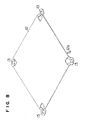
- a shield connecting terminal 12a in the form of an L-shaped configuration as shown in Fig. 8 is provided integrally, and is connected to an earth portion of the circuit module 1, mounting of the roof 12 for electromagnetic shield is easily effected.
- terminal sections 5 and 9 of the respective circuit modules 1 and 2 will next be described in detail.
- the terminal section 5 and the terminal section 9 are only different in terminals 4 and 8 from each other, but are the same as each other in other arrangements. Accordingly, in the following description, only the terminal section 5 will be described with reference to Figs. 9 to 19A and 19B.
- the frame body 3 of the terminal section 5 is provided at an outer edge portion of each of the four frame side portions with a plurality of projecting portions 15 which are spaced apart a predetermined spacing from each other.
- the terminals 4 are extended out from between the projecting portions 15.
- corner portions of the frame body 3 are provided respectively with planar portions 16 which are lower than the projecting portions 15 and the projections 14.
- the frame body 3 is provided, at its underside with four bores 17 reaching respectively the terminals 4, along the sides of the frame body as illustrated in Fig. 11.
- each of the terminals 4 of the terminal section 5 is so bent that a forward end portion thereof extends beyond the frame body 3.
- Each of the terminals 4 has a rearward end portion thereof which is embedded in the frame body 3 as shown in Fig. 14, and projects from the inner peripheral surface of the frame body 3.
- the terminal 4 has an intermediate portion thereof which is so provided as to be planar along an upper surface of the frame body 3 as shown in Figs. 13 to 15, and which is so arranged as to slightly project from the upper surface of the frame body 3.
- the reference numeral 18 denotes a projecting portion projecting from the inner peripheral surface of the frame body 3 for the terminals 4, while the reference numeral 19 denotes a planar portion which is provided at the intermediate portion of a corresponding one of the terminals 4.
- each of the terminals 4 has a boundary portion thereof contiguous to a rearward end portion embedded within the frame body 3 and covered with a resin portion 20.
- each of the terminals 4 of the terminal section 5 is connected to the circuit substrate 7 at the planar portion 19 which projects from the upper surface of the frame body 3 as shown in Fig. 13.
- the outer edges of each of the sides of the circuit substrate 7 abut against the projecting portions 15 of the frame body 3 to attain positioning of the substrate 7 in the frame body 3, whereby it is made possible to position the circuit substrate 7 with respect to the frame body 3, making it possible to accurately and easily effect connection between the terminal section 5 and the circuit substrate 7.
- some out of the plurality of projecting portions 15 may be provided at surfaces thereof, against which the circuit substrate 7 is to abut, with small projections 15a which serve as positioning of the circuit substrate 7. With the arrangement, positioning accuracy can further be improved as compared with a case where positioning is effected by the projecting portions 15.
- a tapering portion 15b is provided on each of the projecting portions 15 to be gradually thinned in an upward direction, so that it is possible to cause the terminals 4 and 8 of the respective terminal sections 5 and 9 to be accurately in coincidence with each other, and electrical and mechanical connection such as soldering or the like at the abutting portions between the terminals 4 and 8 can reliably be effected.
- the frame body 3 of the terminal section 5 is provided at its corners with the projections 14.
- the circuit modules 1 and 2 are piled up each other in a multilayer, the circuit modules can easily be positioned and supported by the projections 14.
- the planar portion 19 of the terminal 4 are partly embedded in the projecting portion 15 as shown in Fig. 17.
- the planar portion 19 of the terminal 4 is fixed by an embedded portion thereof 19a, and accuracy of flatness is secured for the planar portion 19.
- the opposite sides of the planar portion 19 of the terminal 4 are embedded in the projecting portion 15.
- only one side of the planar portion 19 may be embedded in the projecting portion 15 as shown in Fig. 18.
- the terminals 4 are integrally embedded by insert-molding upon molding of the frame body 3.
- the reference numeral 21 denotes terminal frames.
- the opposite ends of each of the plurality of terminals 4 are joined respectively to a pair of connecting portions 21a and 21b. That is, as shown in Fig. 19A, molding of the frame body 3 is effected under such a condition that the four terminal frames 21 are positioned with the connecting portions 21a of the respective terminal frames 21 projecting from the inner peripheral surface of the frame body 3.
- each of the terminals 4 projects from the inner peripheral surface of the frame body 3.
- the use of the terminal frames 21 can accurately effect fixing of the terminals 4 upon insert-molding. Furthermore, bores 17 are provided in the rear surface of the frame body 3, whereby the terminals 4 are held upon insert-molding to enable adequately securing aligning accuracy of the terminals 4.
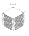
- Fig. 20 shows a second embodiment of the invention.
- nine circuit modules of the first type described above 1 and a single circuit module of the second type described above 2 form an electronic circuit device of ten-layered construction.
- the circuit modules 1 and 2 are the same as those in the above-described first embodiment.
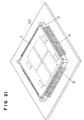
- Fig.21 shows a third embodiment of the invention.
- an electronic circuit device is constituted only by a single circuit module of the second type described above 2.
- the reference numeral 22 denotes a printed wiring board.
- the electronic circuit device according to the embodiment is packaged onto the printed wiring board 22 by soldering or the like, and connection to other electronic circuits is effected.
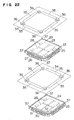
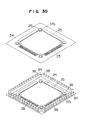
- Fig. 22 to Figs. 24A and 24B show an electronic circuit device according to a fourth embodiment of the invention
- Fig. 25 shows a circuit modules of the electronic circuit device.
- the reference numerals 23 and 24 denote respective circuit modules each in the form of a square plate configuration for forming a predetermined electronic circuit.
- two circuit modules 23 and 24 are used.
- the circuit module 23 comprises a terminal section 27 having a square, annular frame body 25 formed of an insulating material such as synthetic resin and the like and a plurality of terminals 26 provided on the respective frame body portions to extend outwardly of the respective frame body portions and along the side and underside surfaces of the frame body 25 in a C-shaped configuration, and an insulating circuit substrate 29 having wiring patterns each adapted for connection with the respective terminals 26 of the terminal section 27 as by soldering and comprising a member of ceramic and the like, to one surface of which are packaged surface packaging parts 28 such as flip-chip type semiconductors, resistors, capacitors.and the like.
- the reference numeral 29a denotes a connecting land portion to which the terminals 26 are soldered, and which is arranged on a peripheral edge portion of the circuit substrate 29 in agreement with the arrangement of the terminals 26.
- the circuit module 24 comprises, similarly to the circuit module 23, a terminal section 31 having a frame body 25 and a plurality of terminals 30 provided on the respective frame body portions to extend outwardly of the respective frame body portions and along the side and underside surfaces of the frame body 25 in a L-shaped configuration to assume a gull-wing shape, and an insulating circuit substrate 29 mounting thereon a circuit identical to or different from that of the circuit substrate 29 of the circuit module 23.
- the circuit substrates 29 are connected to the terminal sections 27 and 31 such that the side where the parts are surface packaged is directed inwardly of the terminal sections 27 and 31. Further, the terminal sections 27 and 31 have respective thicknesses thereof such that the surface packaging parts 28 of the circuit substrate 29 do not extend beyond the terminal sections 27 and 31.
- the circuit modules 23 and 24 are positioned such that the terminals 26 and 30 of the respective terminal sections 27 and 31 are in registration with each other, and are piled up each other such that the circuit module 23 is overlapped on the circuit module 24.
- the terminals 26 and 30 of the respective circuit modules 23 and 24 are electrically and mechanically connected to each other at abutment portions by soldering or the like.
- the reference numeral 32 denotes a connecting areas where the terminals 26 are connected respectively to the terminals 30; and 33, connecting areas where the terminals 26 and 30 are connected respectively to connecting land portions 29a of the wiring patterns of the circuit substrates 29.
- Heat-radiating plates 34 in the form of a square plate configuration made of metal are arranged respectively at the tops of the respective circuit modules 23 and 24 piled up each other in this manner through silicon grease or the like, to thereby effect heat radiation of the circuit modules 23 and 24.
- the heat-radiating plates 34 are larger in area than the circuit modules 23 and 24, respectively.
- Windows 35 are provided in the heat-radiating plates 34 to correspond to upper portions of the terminal sections 27 and 31 so as to provide image-recognition of the terminals 26 and 30 when the electronic circuit device is packaged.
- fixing bores 36 are formed in corner portions of the heat-radiating plates 34, for fixing the heat radiating plates 34 respectively to the frame bodies 25 of the circuit modules 23 and 24 by caulking.
- projections 37 are provided respectively at the corner portions of the frame bodies 25 of the respective circuit modules 23 and 24.
- the fixing bores 36 in the heat radiating plate 34 are fitted respectively over the projections 37.
- the projections 37 are pressed to caulk the heat-radiating plates 34 respectively to the projections 37 of the frame bodies 25.
- the heat-radiating plates 34 are fixed respectively to the frame bodies 25.
- the reference numeral 37a denote caulked portions which are provided respectively by pressing of the projections 37.
- projections 34a are provided respectively on the heat-radiating plates 34 as shown in Fig.
- heat-radiating plates 34 and the surface packaging parts 28 are in direct contact with each other through silicon grease or the like, to thereby improve heat-radiation advantages or effects.
- the lowermost heat-radiating plate 34 is held by a peripheral portion 34b, which is folded back in the form of an L-shaped configuration, of a heat-radiating plate 34 disposed on the circuit module 24.
- heat sinks 38 in the form of a comb may be arranged between upper and lower heat-radiating plates 34, to improve heat-radiating advantages. With the arrangement, heat radiation can reliably be effected as compared with the case where the heat-radiating plates 34 and the substrates are in direct contact respectively with each other to radiate heat.
- terminal sections 27 and 31 of the respective circuit modules 23 and 24 will next be described in detail.
- the terminal section 27 and the terminal section 31 are different from each other only in the terminals 26 and 30, and are the same as each other in terms of the remaining constitution.
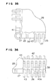
- only the terminal section 27 will be described with reference to Figs. 32 to 36.
- the frame body 25 of the terminal section 27 is provided at outer edge portions of upper portions of four respective frame sections with projecting portions 39 which serve as effecting positional regulation at an outer end.
- a plurality of grooves 40 are provided on the outer side of the projecting portions 39 with predetermined spaces left therebetween outwardly.
- the terminals 26 are taken out through the grooves 40, respectively.
- each of the terminals 26 of the terminal section 27 is bent to have forward ends thereof project outwardly from the frame body 25.
- the respective rearward ends of terminals 26 are embedded in the frame body 25 to project from the inner peripheral surface of the frame body 25.
- intermediate portions of the respective terminals 26 are so provided as to become planar along the upper surface of the frame body 25 as shown in Figs. 33 to 35, and are so arranged as to project slightly from the upper surface of the frame body 25.
- the reference numeral 42 denotes projecting portions of the terminals 26 projecting from the inner peripheral surface of the frame body 25, while 43 denotes planar portions provided respectively at the intermediate portions of the terminals 26.
- boundary portions between the planar portions 43 of the respective terminals 26 and the rearward end portion embedded in the frame body 25 are covered respectively with resin portions 44.
- terminals 26 of the terminal section 27 are connected to the circuit substrate 29 at the planar portions 43 which project from the upper surface of the frame body 25 as shown in Fig. 33.
- the outward side edges of the circuit substrate 29 abut respectively against the projecting portions 39 of the frame body 25 to thereby be positioned, whereby it is possible to position the circuit substrate 29 with respect to the frame body 25 and to accurately and easily effect connection between the terminal sections 27 and the circuit substrate 29.
- four corners of the projecting portions 39 are relieved in a manner not to abut against the substrate whereby interference between the flash of the substrate and the projecting portions are prevented from occurring. Thus, it is possible to effect connection accurately.
- planar portions 43 of the respective terminals 26 are partly embedded in the projecting portions 39 as shown in Fig. 36.
- the planar portions 43 of the respective terminals 26 are fixed by the embedded portions 43a, and accuracy of flatness for planar portions 43 is secured thereby.
- a circuit module comprises a terminal section having a annular insulating frame body and a plurality of terminals provided on the respective frame body portions to extend outwardly therefrom, and an circuit substrate having wiring patterns each adapted for connection with the respective terminals of the terminal section and packaging to one surface thereof surface packaging parts with the surface packaging parts directed toward the inside of the terminal section.
- a plurality of these circuit modules are stacked on one another and are connected to one another by terminals, so that high-density packaging circuit substrates can be readily connected to one another by the terminal sections with accuracy whereby the circuit modules can be readily and accurately arranged in a multi-layered manner to enable realizing high-density packaging.
Landscapes
- Engineering & Computer Science (AREA)
- Microelectronics & Electronic Packaging (AREA)
- Combinations Of Printed Boards (AREA)
- Structure Of Printed Boards (AREA)
Claims (19)
- Dispositif de circuit électronique comprenant :au moins un premier module de circuit (1) comprenant (i) une première section de bornes (5) ayant un premier corps de cadre annulaire isolant (3) et une première pluralité de bornes (4) présentes sur ledit premier corps annulaire isolant (3) pour s'étendre vers l'extérieur à partir dudit corps de cadre annulaire isolant (3) suivant une configuration en forme de C, et (ii) un premier substrat de circuit (7) ayant une première pluralité de dessins de câblage adapté pour être connecté au bornes de la première pluralité de bornes (4), ledit premier substrat de circuit (7) ayant une surface sur laquelle sont montées des premières parties en boíte (6) qui sont connectées aux dites bornes de la première pluralité (4) par l'intermédiaire desdits dessins de câblage de la première pluralité de telle façon que le côté du substrat (7) où les parties (6) sont montées est orienté vers l'intérieur de la section de borne (5) ;un second module de circuit (2) comprenant (i) une seconde section de bornes (9) ayant un second corps de cadre annulaire isolant (3) et une seconde pluralité de bornes (8) présentes sur ledit second corps de cadre annulaire isolant (3) pour s'étendre vers l'extérieur à partir dudit second corps de cadre annulaire isolant (3) suivant une configuration en forme de L, et (ii) un second substrat de circuit (7) ayant une seconde pluralité de dessins de câblage adapté pour être connecté aux bornes de la seconde pluralité (8), ledit second substrat de circuit (7) ayant une surface sur laquelle sont montées les secondes parties en boíte (6) qui sont connectées aux bornes de ladite seconde pluralité (8) par l'intermédiaire des dessins de câblage de ladite seconde pluralité de telle façon que le côté du substrat (7) où les parties (6) sont montées est orienté vers l'intérieur de la section de borne (9) ; caractérisé en ce qu'au moins un premier module de circuit (1) est empilé sur ledit second module de circuit (2) pour obtenir des modules de circuit empilés, ledit second module de circuit (2) étant installé au niveau d'une zone la plus basse desdits modules de circuit empilés, et le premier et le second modules de circuit (1, 2) étant connectés l'un à l'autre par prise directe desdites première et seconde pluralités de bornes (4, 8) ; et en ce que chaque borne (4, 8, 26, 30) desdites première et seconde pluralités de bornes possède une partie (19, 43) prévue le long d'une surface du corps de cadre annulaire isolant respectif (3, 25), laquelle partie possède une zone de connexion (11, 33) destinée à être connectée aux dessins de câblage respectifs.
- Dispositif de circuit électronique selon la revendication 1, dans lequel des plaques de radiation de chaleur (34) destinées à la radiation de chaleur sont prévues pour venir en butée contre les substrats de circuit (7) des modules de circuit respectifs (1, 2).
- Dispositif de circuit électronique selon la revendication 2, dans lequel une borne de connexion destinée à un écran de protection électromagnétique est prévue sur chacune desdites plaques de radiation de chaleur (34).
- Dispositif de circuit électronique selon la revendication 2, dans lequel lesdites plaques de radiation de chaleur sont pourvues de fenêtres (35) qui sont positionnées pour correspondre aux bornes (26, 30) des première et seconde sections de bornes respectives (27, 31).
- Dispositif de circuit électronique selon la revendication 2, dans lequel lesdites plaques de radiation de chaleur (34) sont pourvues d'un bossage ou de bossages (34a) pour faire en sorte que lesdites plaques de radiation de chaleur (34) et lesdites première et seconde parties en boíte (6) soient en contact direct les uns avec les autres.
- Dispositif de circuit électronique selon la revendication 1, dans lequel les bossages (14) sont présents au niveau des coins des corps de cadre respectifs (3) des premier et second modules de circuit respectifs (1, 2), lesquels bossages (14) servent à supporter lesdits modules de circuit empilés (1, 2) de manière à être écartés.
- Dispositif de circuit électronique selon la revendication 1, dans lequel lesdites première et seconde sections de borne (5, 9) sont présentes au niveau des parties supérieures et périphériques des corps de cadre respectifs (3) avec une pluralité de parties en saillie (15) qui servent à effectuer le réglage positionnel des extrémités extérieures des substrats de circuit respectifs (7) et qui sont disposées avec des espacements prédéterminés entre elles, et dans lequel une pluralité de bornes (4, 8) sont sorties à travers et entre les parties en saillie.
- Dispositif de circuit électronique selon la revendication 2, dans lequel ledit corps de cadre annulaire isolant (3) de chacune desdites première et seconde sections de bornes (5, 9) comprend une pluralité de parties en saillie (15) disposées sur les bords extérieurs d'une surface supérieure dudit corps de cadre annulaire isolant (3), et dans lequel chaque borne desdites première et seconde pluralités de bornes (4, 8) est disposée entre deux desdites parties en saillie.
- Dispositif de circuit électronique selon la revendication 7 ou 8, dans lequel les parties en saillie (15) présentes sur lesdites première et seconde sections de borne (5, 9) sont coniques.
- Dispositif de circuit électronique selon la revendication 9, dans lequel les parties en saillie (15) desdites première et seconde sections de bornes (5, 9) destinées à positionner lesdits substrats de circuit (7) sont évidées au niveau des quatre coins de celles-ci (16) pour ne pas être en contact avec lesdits substrats de circuit (7) au niveau des parties évidées.
- Dispositif de circuit électronique selon la revendication 1, dans lequel les bornes (4, 8) sont prévues pour être moulées par insert dans ledit corps de cadre (3) dans les dites première et seconde sections de borne (5, 9).
- Dispositif de circuit électronique selon la revendication 9, dans lequel les bornes (4, 8) desdites première et seconde sections de bornes (5, 9) sont structurées de telle façon que les parties de celles-ci qui sont proches des extrémités arrière sont encastrées dans ledit corps de cadre (3), les extrémités arrière étant en saillie à partir de la surface périphérique intérieure dudit corps de cadre (3), et dans lequel les parties plates à la moitié de la longueur desdites bornes (4, 8) sont disposées au-dessus de la surface supérieure dudit corps de cadre (3) et sont étendues vers la périphérie dudit corps de cadre (3) à travers et entre les dites parties en saillie (15).
- Dispositif de circuit électronique selon la revendication 9, dans lequel les parties des bornes (4, 8) disposées entre lesdites parties en saillie (15) sont partiellement encastrées dans lesdites parties en saillie (15).
- Dispositif de circuit électronique selon la revendication 9, dans lequel des petits bossages (15a) sont présents sur les surfaces desdites parties en saillie (15) dudit corps de cadre (3) avec lesquelles les bords extérieurs desdits substrats de circuit (7) sont en prise.
- Dispositif de circuit électronique selon la revendication 1, dans lequel lesdites première et seconde sections de borne (5, 9) sont structurées de telle façon que des ouvertures (17) sont formées dans les parties de dessous dudit corps de cadre (3) pour conduire vers lesdites bornes.
- Procédé de fabrication d'un circuit électronique comprenant les étapes :de préparation d'au moins un premier module de circuit (1) comprenant (i) une première section de borne (5) ayant un premier corps de cadre annulaire isolant (3) et une première pluralité de bornes (4) présentes sur ledit corps annulaire isolant (3) pour s'étendre vers l'extérieur à partir dudit premier corps de cadre annulaire isolant (3) suivant une configuration en forme de C, et (ii) un premier substrat de circuit (7) ayant une première pluralité de dessins de câblage adapté pour être connecté aux bornes de la première pluralité (4), ledit premier substrat de circuit (7) ayant une surface sur laquelle sont montées des premières parties en boíte (6) qui sont connectées aux dites bornes de la première pluralité (4) par l'intermédiaire des dessins de câblage de ladite première pluralité de telle façon que le côté du substrat (7) où les parties (6) sont montées est orienté vers l'intérieur de la section de bornes (5), chaque borne (4) de ladite première pluralité ayant une partie (19) prévue le long d'une surface du premier corps de cadre annulaire isolant (3), laquelle partie possède une zone de connexion (11) destinée à la connexion aux dessins de câblage de la première pluralité ;de préparation d'un second module de circuit (2) comprenant (i) une seconde section de bornes (9) ayant un second corps de cadre annulaire isolant (3) et une seconde pluralité de bornes (8) présentes sur ledit second corps de cadre annulaire isolant (3) pour s'étendre vers l'extérieur à partir dudit second corps de cadre annulaire isolant (3) suivant une configuration en forme de L, et (ii) un second substrat de circuit (7) ayant une seconde pluralité de dessins de câblage conçu pour être connecté aux bornes de la seconde pluralité (8), ledit second substrat de circuit (7) ayant une surface sur laquelle sont montées des secondes parties en boíte (6) qui sont connectées aux dites bornes de la seconde pluralité (8) par l'intermédiaire des dessins de câblage de ladite seconde pluralité de telle façon que le côté du substrat (7) où les parties (6) sont montées est orienté vers l'intérieur de la section de bornes (9), chaque borne (8) de ladite seconde pluralité ayant une partie (19) prévue le long d'une surface du second corps de cadre annulaire isolant (3), laquelle partie possède une zone de connexion (11) destinée à être connectée aux dessins de câblage de la seconde pluralité ; etd'empilage dudit au moins premier module de circuit (1) sur ledit second module de circuit (2) pour obtenir des modules de circuit empilés, ledit second module de circuit (2) étant disposé au niveau d'une zone la plus basse desdits modules de circuit empilés, et le premier et le second modules de circuit (1, 2) étant connectés l'un à l'autre par prise directe des bornes desdites première et seconde pluralités 4, 8) ; où les étapes de préparation des premier et second modules de circuit comprennent les étapes :de préparation de cadres de borne (21) comprenant les pluralités respectives de bornes (4, 8), chaque cadre de borne comprenant un nombre respectif de bornes de la pluralité respective de bornes, les premières parties de connexion (21a) connectant les premières extrémités dudit nombre respectif de bornes et les secondes parties de connexion (21b) connectant lesdites secondes extrémités dudit nombre respectif de bornes ;de moulage par insert desdits cadres de borne (21) dans les corps de cadre annulaire isolant respectif (3) tandis que les premières parties de connexion (21a) au niveau d'une première extrémité desdits cadres de borne (21) sont en saillie à partir de la surface périphérique intérieure desdits corps de cadre annulaire isolant respectifs ; etde découpage desdites parties de connexion (21a, 21b).
- Dispositif de circuit électronique comprenant :
un module de circuit (1) comprenant (i) une section de bornes (5) ayant un corps de cadre annulaire isolant (3) et une pluralité de bornes (4) présentes sur ledit corps annulaire isolant (3) pour s'étendre vers l'extérieur à partir dudit corps de cadre annulaire isolant (3), et (ii) un substrat de circuit (7) ayant une pluralité de dessins de câblage adapté pour être connecté aux bornes de la pluralité (4), ledit substrat de circuit (7) ayant une surface sur laquelle sont montées des parties en boíte (6) qui sont connectées aux bornes de ladite pluralité (4) par l'intermédiaire des dessins de câblage de ladite pluralité de telle façon que le côté du substrat (7) où les parties sont montées est orienté vers l'intérieur de la section de bornes (5), caractérisé en ce que chacune desdites bornes (4) possède une partie (19) prévue le long d'une surface du corps de cadre annulaire isolant (3), laquelle partie possède une zone de connexion (11) destinée à être connectée aux dessins de câblage. - Dispositif de circuit électronique selon la revendication 1, comprenant un moyen de couverture (12) destiné à obtenir une protection électromagnétique, au-dessus dudit au moins un premier module de circuit (1).
- Procédé de fabrication d'un circuit électronique selon la revendication 16 comprenant l'étape supplémentaire de réalisation d'un moyen de couverture (12) destiné à obtenir une protection électromagnétique au-dessus dudit au moins un premier module de circuit (1).
Applications Claiming Priority (6)
| Application Number | Priority Date | Filing Date | Title |
|---|---|---|---|
| JP5029292 | 1992-03-09 | ||
| JP50292/92 | 1992-03-09 | ||
| JP5029292 | 1992-03-09 | ||
| JP14724592 | 1992-06-08 | ||
| JP14724592 | 1992-06-08 | ||
| JP147245/92 | 1992-06-08 |
Publications (3)
| Publication Number | Publication Date |
|---|---|
| EP0560502A2 EP0560502A2 (fr) | 1993-09-15 |
| EP0560502A3 EP0560502A3 (en) | 1995-09-13 |
| EP0560502B1 true EP0560502B1 (fr) | 2001-08-29 |
Family
ID=26390749
Family Applications (1)
| Application Number | Title | Priority Date | Filing Date |
|---|---|---|---|
| EP93301216A Expired - Lifetime EP0560502B1 (fr) | 1992-03-09 | 1993-02-19 | Dispositif de circuits électroniques et procédé de fabrication |
Country Status (5)
| Country | Link |
|---|---|
| US (1) | US5346402A (fr) |
| EP (1) | EP0560502B1 (fr) |
| KR (1) | KR970004025B1 (fr) |
| DE (1) | DE69330657T2 (fr) |
| TW (1) | TW212261B (fr) |
Families Citing this family (16)
| Publication number | Priority date | Publication date | Assignee | Title |
|---|---|---|---|---|
| JPH07142673A (ja) * | 1993-11-15 | 1995-06-02 | Matsushita Electric Ind Co Ltd | 集積回路装置 |
| US5643000A (en) * | 1994-09-27 | 1997-07-01 | Intel Corporation | Method and apparatus for providing processor field upgradability to a motherboard |
| US5677830A (en) * | 1995-03-02 | 1997-10-14 | Mitel Corporation | Modular, stacking, expandable electronic enclosure system |
| USD416872S (en) * | 1997-11-06 | 1999-11-23 | Zf Microsystems, Inc. | Single component computer |
| US6849480B1 (en) | 1999-05-07 | 2005-02-01 | Seagate Technology Llc | Surface mount IC stacking method and device |
| US6707684B1 (en) * | 2001-04-02 | 2004-03-16 | Advanced Micro Devices, Inc. | Method and apparatus for direct connection between two integrated circuits via a connector |
| GB2379330A (en) * | 2001-08-29 | 2003-03-05 | Motorola Inc | Package for electronic components and method for forming a package for electronic components |
| JP4177571B2 (ja) | 2001-09-20 | 2008-11-05 | 三菱電機株式会社 | 半導体装置 |
| JP4209130B2 (ja) * | 2002-04-09 | 2009-01-14 | 株式会社ザナヴィ・インフォマティクス | 多層モジュール基板 |
| FR2845821B1 (fr) * | 2002-10-11 | 2005-12-02 | Thales Sa | Substrat electronique d'un module electronique a trois dimensions a fort pouvoir de dissipation thermique et module electronique |
| DE102004012979B4 (de) * | 2004-03-16 | 2009-05-20 | Infineon Technologies Ag | Kopplungssubstrat für Halbleiterbauteile, Anordnungen mit dem Kopplungssubstrat, Kopplungssubstratstreifen, Verfahren zur Herstellung dieser Gegenstände und Verfahren zur Herstellung eines Halbleitermoduls |
| US7258552B2 (en) * | 2005-07-05 | 2007-08-21 | Hewlett-Packard Development Company, L.P. | Socket for holding a circuit board module |
| JP4720827B2 (ja) * | 2005-07-11 | 2011-07-13 | パナソニック株式会社 | 基板接続部材および接続構造体 |
| WO2008035442A1 (fr) * | 2006-09-22 | 2008-03-27 | Panasonic Corporation | Dispositif de circuit, procédé de fabrication de dispositif de circuit et élément de connexion |
| CN101190552A (zh) * | 2006-11-29 | 2008-06-04 | 深圳富泰宏精密工业有限公司 | 模具结构 |
| EP2883432A4 (fr) * | 2012-08-10 | 2016-05-11 | Ericsson Telefon Ab L M | Module radio et procédé de fabrication associé |
Family Cites Families (10)
| Publication number | Priority date | Publication date | Assignee | Title |
|---|---|---|---|---|
| GB1207728A (en) * | 1968-11-27 | 1970-10-07 | Standard Telephones Cables Ltd | Housing assembly for an electric circuit |
| US3771109A (en) * | 1972-05-01 | 1973-11-06 | Bunker Ramo | Electrical connector for integrated circuit device |
| USRE32370E (en) * | 1981-02-02 | 1987-03-10 | Amp Incorporated | Low height ADS connector |
| US4433886A (en) * | 1981-12-17 | 1984-02-28 | Elco Corporation | Connector mounting for integrated circuit chip packages |
| US4648666A (en) * | 1985-07-03 | 1987-03-10 | Amp Incorporated | Electrical connector |
| JPS63502866A (ja) * | 1986-03-25 | 1988-10-20 | ダウティ エレクトロニック コンポ−ネンツ リミティド | 電気回路の相互接続システム |
| GB2196178B (en) * | 1986-10-09 | 1990-04-11 | Amp Inc | Semiconductor chip carrier system |
| US4890199A (en) * | 1988-11-04 | 1989-12-26 | Motorola, Inc. | Miniature shield with opposing cantilever spring fingers |
| JPH07105628B2 (ja) * | 1989-11-18 | 1995-11-13 | シャープ株式会社 | 電子部品の実装方法 |
| JPH0423396A (ja) * | 1990-05-14 | 1992-01-27 | Fujitsu Ltd | プリント基板の実装構造 |
-
1992
- 1992-12-16 TW TW081110084A patent/TW212261B/zh active
-
1993
- 1993-02-19 US US08/019,671 patent/US5346402A/en not_active Expired - Fee Related
- 1993-02-19 EP EP93301216A patent/EP0560502B1/fr not_active Expired - Lifetime
- 1993-02-19 DE DE69330657T patent/DE69330657T2/de not_active Expired - Fee Related
- 1993-03-08 KR KR93003417A patent/KR970004025B1/ko not_active Expired - Fee Related
Also Published As
| Publication number | Publication date |
|---|---|
| EP0560502A3 (en) | 1995-09-13 |
| TW212261B (en) | 1993-09-01 |
| US5346402A (en) | 1994-09-13 |
| KR930021040A (ko) | 1993-10-20 |
| KR970004025B1 (en) | 1997-03-24 |
| DE69330657D1 (de) | 2001-10-04 |
| DE69330657T2 (de) | 2002-07-04 |
| EP0560502A2 (fr) | 1993-09-15 |
Similar Documents
| Publication | Publication Date | Title |
|---|---|---|
| US5346402A (en) | Electronic circuit device and manufacturing method thereof | |
| US10249550B2 (en) | Power module with lead component and manufacturing method thereof | |
| JP2724312B2 (ja) | Icチップ・キャリアパッケージ | |
| US5723903A (en) | Thin type semiconductor device, module structure using the device and method of mounting the device on board | |
| US5781415A (en) | Semiconductor package and mounting method | |
| KR20010034154A (ko) | 다수의 기판층과 적어도 하나의 반도체 칩을 가진 반도체소자 및 그의 제조 방법 | |
| US10757845B2 (en) | High-frequency component provided with a shield case | |
| US7217991B1 (en) | Fan-in leadframe semiconductor package | |
| JPH06125021A (ja) | 面実装型ダイオード | |
| US6818974B2 (en) | Semiconductor device | |
| JP2002506289A (ja) | 多数の半導体チップを有する半導体素子 | |
| JPS6348183B2 (fr) | ||
| JP2001196526A (ja) | マルチベアチップ実装体、マルチチップパッケージ、半導体装置、ならびに電子機器 | |
| US20050030723A1 (en) | Fully-molded or lidded circuit module assembly having edge-stiffening interlock features | |
| JP3232723B2 (ja) | 電子回路装置およびその製造方法 | |
| CN210722994U (zh) | 电子元件的封装结构 | |
| JP2524482B2 (ja) | Qfp構造半導体装置 | |
| US20070246809A1 (en) | Package for optical device and method of manufacturing the same | |
| JPH0982826A (ja) | 半導体素子封止用パッケージおよびそれを用いた回路装置の実装構造 | |
| JP2722451B2 (ja) | 半導体装置 | |
| JP3769881B2 (ja) | 電子回路装置 | |
| US12482737B2 (en) | Intelligent power module package structure and hybrid ceramic board | |
| US5677571A (en) | Semiconductor package having reinforced lead pins | |
| TWI913023B (zh) | 半導體封裝模組、導電連接元件及其製造方法 | |
| US20260066174A1 (en) | Power module |
Legal Events
| Date | Code | Title | Description |
|---|---|---|---|
| PUAI | Public reference made under article 153(3) epc to a published international application that has entered the european phase |
Free format text: ORIGINAL CODE: 0009012 |
|
| AK | Designated contracting states |
Kind code of ref document: A2 Designated state(s): DE FR GB |
|
| PUAL | Search report despatched |
Free format text: ORIGINAL CODE: 0009013 |
|
| AK | Designated contracting states |
Kind code of ref document: A3 Designated state(s): DE FR GB |
|
| 17P | Request for examination filed |
Effective date: 19960126 |
|
| 17Q | First examination report despatched |
Effective date: 19981208 |
|
| GRAG | Despatch of communication of intention to grant |
Free format text: ORIGINAL CODE: EPIDOS AGRA |
|
| GRAG | Despatch of communication of intention to grant |
Free format text: ORIGINAL CODE: EPIDOS AGRA |
|
| GRAH | Despatch of communication of intention to grant a patent |
Free format text: ORIGINAL CODE: EPIDOS IGRA |
|
| GRAH | Despatch of communication of intention to grant a patent |
Free format text: ORIGINAL CODE: EPIDOS IGRA |
|
| GRAG | Despatch of communication of intention to grant |
Free format text: ORIGINAL CODE: EPIDOS AGRA |
|
| GRAH | Despatch of communication of intention to grant a patent |
Free format text: ORIGINAL CODE: EPIDOS IGRA |
|
| GRAA | (expected) grant |
Free format text: ORIGINAL CODE: 0009210 |
|
| AK | Designated contracting states |
Kind code of ref document: B1 Designated state(s): DE FR GB |
|
| REF | Corresponds to: |
Ref document number: 69330657 Country of ref document: DE Date of ref document: 20011004 |
|
| ET | Fr: translation filed | ||
| REG | Reference to a national code |
Ref country code: GB Ref legal event code: IF02 |
|
| PLBE | No opposition filed within time limit |
Free format text: ORIGINAL CODE: 0009261 |
|
| STAA | Information on the status of an ep patent application or granted ep patent |
Free format text: STATUS: NO OPPOSITION FILED WITHIN TIME LIMIT |
|
| 26N | No opposition filed | ||
| PGFP | Annual fee paid to national office [announced via postgrant information from national office to epo] |
Ref country code: FR Payment date: 20050208 Year of fee payment: 13 |
|
| PGFP | Annual fee paid to national office [announced via postgrant information from national office to epo] |
Ref country code: GB Payment date: 20050216 Year of fee payment: 13 |
|
| PGFP | Annual fee paid to national office [announced via postgrant information from national office to epo] |
Ref country code: DE Payment date: 20050217 Year of fee payment: 13 |
|
| PG25 | Lapsed in a contracting state [announced via postgrant information from national office to epo] |
Ref country code: GB Free format text: LAPSE BECAUSE OF NON-PAYMENT OF DUE FEES Effective date: 20060219 |
|
| PG25 | Lapsed in a contracting state [announced via postgrant information from national office to epo] |
Ref country code: DE Free format text: LAPSE BECAUSE OF NON-PAYMENT OF DUE FEES Effective date: 20060901 |
|
| GBPC | Gb: european patent ceased through non-payment of renewal fee |
Effective date: 20060219 |
|
| REG | Reference to a national code |
Ref country code: FR Ref legal event code: ST Effective date: 20061031 |
|
| PG25 | Lapsed in a contracting state [announced via postgrant information from national office to epo] |
Ref country code: FR Free format text: LAPSE BECAUSE OF NON-PAYMENT OF DUE FEES Effective date: 20060228 |