EP0560659A1 - Verfahren und Vorrichtung zur optischen Übertragung eines Multiplexsignals mit elektrischen Trägern - Google Patents
Verfahren und Vorrichtung zur optischen Übertragung eines Multiplexsignals mit elektrischen Trägern Download PDFInfo
- Publication number
- EP0560659A1 EP0560659A1 EP93400579A EP93400579A EP0560659A1 EP 0560659 A1 EP0560659 A1 EP 0560659A1 EP 93400579 A EP93400579 A EP 93400579A EP 93400579 A EP93400579 A EP 93400579A EP 0560659 A1 EP0560659 A1 EP 0560659A1
- Authority
- EP
- European Patent Office
- Prior art keywords
- signal
- electrical
- multiplex
- optical
- dissymmetrization
- Prior art date
- Legal status (The legal status is an assumption and is not a legal conclusion. Google has not performed a legal analysis and makes no representation as to the accuracy of the status listed.)
- Granted
Links
- 230000003287 optical effect Effects 0.000 title claims abstract description 61
- 239000000969 carrier Substances 0.000 title claims abstract description 25
- 238000000034 method Methods 0.000 title claims abstract description 22
- 230000005540 biological transmission Effects 0.000 title claims abstract description 15
- 238000001228 spectrum Methods 0.000 claims abstract description 18
- 230000003111 delayed effect Effects 0.000 claims abstract description 6
- 238000001914 filtration Methods 0.000 claims description 22
- 239000013307 optical fiber Substances 0.000 claims description 7
- 238000006243 chemical reaction Methods 0.000 claims description 4
- 238000001514 detection method Methods 0.000 claims description 4
- 239000000835 fiber Substances 0.000 description 7
- 230000035945 sensitivity Effects 0.000 description 6
- 230000003595 spectral effect Effects 0.000 description 6
- 230000003321 amplification Effects 0.000 description 5
- 238000003199 nucleic acid amplification method Methods 0.000 description 5
- 239000003990 capacitor Substances 0.000 description 2
- 238000004519 manufacturing process Methods 0.000 description 2
- 239000004065 semiconductor Substances 0.000 description 2
- 239000000470 constituent Substances 0.000 description 1
- 238000010586 diagram Methods 0.000 description 1
- 238000003780 insertion Methods 0.000 description 1
- 230000037431 insertion Effects 0.000 description 1
- 108091008695 photoreceptors Proteins 0.000 description 1
- 230000000284 resting effect Effects 0.000 description 1
- 230000002123 temporal effect Effects 0.000 description 1
Images


Classifications
-
- H—ELECTRICITY
- H04—ELECTRIC COMMUNICATION TECHNIQUE
- H04B—TRANSMISSION
- H04B10/00—Transmission systems employing electromagnetic waves other than radio-waves, e.g. infrared, visible or ultraviolet light, or employing corpuscular radiation, e.g. quantum communication
- H04B10/25—Arrangements specific to fibre transmission
- H04B10/2507—Arrangements specific to fibre transmission for the reduction or elimination of distortion or dispersion
-
- H—ELECTRICITY
- H04—ELECTRIC COMMUNICATION TECHNIQUE
- H04N—PICTORIAL COMMUNICATION, e.g. TELEVISION
- H04N7/00—Television systems
- H04N7/22—Adaptations for optical transmission
Definitions
- the subject of the present invention is a method of optical transmission, by modulation of the power of the optical carrier, of a multiplex or group of electrical carriers comprising an unoccupied range in the lower part of its frequency spectrum.
- the invention also relates to a device implementing this method.
- This invention finds a particularly interesting application in optical fiber transmission systems of a multiplex of analog or digital carriers, in particular for the transmission and distribution of television channels in MABLR (Residual Sideband Amplitude Modulation).
- MABLR Residual Sideband Amplitude Modulation
- optical technology for the transmission and distribution of video channels in the form of a multiplex of MABLR carriers is beginning to enter an industrial phase. This has been made possible by recent advances in optical sources in terms of linearity and RIN (Relative Intensity Noise). Furthermore, erbium-doped fiber optical amplifiers are very suitable for analog signals because they are very linear as soon as the modulation frequency of the optical signal exceeds a few kilohertz. Installed online or as a transmission amplifier, they make it possible to obtain, thanks to their high gain and high output power, an energy budget sufficient to both establish long ranges and distribute the optical energy to several points. reception by means of optical couplers.
- any means allowing an increase in the energy budget is of interest. Indeed, this increase can be used to increase the range between two line amplifiers as well as the sharing rate of the optical source, which leads to cost savings.
- the present invention aims to increase the energy budget of optical systems carrying a multiplex of electric carriers.
- the electrical signal corresponding to a carrier multiplex has a low amplitude for a large percentage of the time and a large amplitude for a small percentage of the time.
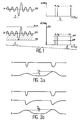
- Such an electrical signal is represented in a simplified manner, for better graphic clarity, by the electrical signal A, symmetrical with respect to its rest point PR, of the appended figure.
- FIG. 1 shows an example of a frequency spectrum A ′ corresponding to the signal A and composed of n carriers, ie P1 to Pn.
- n carriers ie P1 to Pn.
- there is an unoccupied range between the frequency F 0 and the frequency of the first carrier P1.
- Signal B is here represented at the limit of clipping, both in the vicinity of maximum instantaneous power and of zero power, and it is recalled that the clipping of such a signal generates intermodulation distortion . It is noted, by observing the hatched part which represents the optical energy, that the optical modulation rate is low for a large percentage of the time. This is reflected, on the frequency spectrum B ′, represented in FIG.
- the object of the present invention is precisely to remedy this drawback.
- the object of the invention is to allow a reduction in the spectral density of shot noise and therefore an increase in the carrier-to-noise ratio at the output of the optical receiver.
- the invention proposes, for this purpose, a method which consists, from the electrical signal corresponding to a carrier multiplex, to produce an electrical dissymmetrization signal whose frequency spectrum is included in the unoccupied range located in the lower part of the spectrum frequency of said multiplex of electrical carriers, adding this dissymmetry electrical signal to the electrical signal corresponding to said previously delayed multiplex and modulating in power an optical source by the asymmetrical electrical signal thus obtained.
- An advantage of this method is that the spectral density of shot noise is lower. This advantage results in an increase in the carrier-to-noise ratio at the output of the receiver. optical and therefore leads to an improvement in sensitivity.
- said optical source is power-modulated by the asymmetrical electrical signal obtained, relative to its positive and negative half-waves with respect to its rest point, with a modulation polarity which matches minima, respectively maxima, of optical power with half-waves. of low amplitude, respectively of high amplitude, of said asymmetrical electrical signal.
- one mode of obtaining an electrical dissymmetrization signal consists in detecting, on the electrical signal corresponding to the multiplex to be transmitted, the amplitudes lower, respectively higher, at a threshold situated below, respectively above, from its quiescent point, perform bandpass filtering of the signal from the previous detection, in a frequency band included in the unoccupied range of the frequency spectrum of said multiplex and to invert and amplify the signal resulting from the preceding filtering.
- An advantageous variant of the preceding method of obtaining consists in carrying out the same operations and, moreover, in temporarily maintaining the peak values of the signal resulting from the detection prior to filtering.
- the invention also relates to a device for implementing this method. It comprises means for distributing the electrical signal corresponding to the multiplex to be transmitted over two outputs, means for producing an electrical dissymmetrization signal, means for delaying the electrical signal corresponding to said multiplex, means for adding this delayed electrical signal to said electrical signal dissymmetrization and a means of electro-optical conversion that is modular in power.
- the means for producing an electrical dissymmetrization signal comprises a threshold detector receiving an electrical signal corresponding to the multiplex to be transmitted and supplying a bandpass filter connected to the input of an inverting amplifier.
- the means for producing an electrical dissymmetrization signal may further comprise means for temporarily maintaining peak values.
- the electro-optical power conversion means comprises an optical fiber amplifier at the output.
- Optical sources such as a directly modulated laser diode or a continuously operating laser followed by an external modulator deliver instantaneous optical power which is limited to a maximum value.
- a fiber optic amplifier is limited in terms of average optical power and is capable of providing very high instantaneous optical power. It should also be noted that this advantage manifests itself in the same way when the optical fiber amplifier is used as a line amplifier.
- FIG. 2 shows the temporal forms of electrical signals: A, C, D and E, and of optical signals: F and G, as well as the corresponding frequency spectra, respectively: A ', C', D ' , E ', F' and G '.
- the signal A identical to the signal A in FIG. 1, corresponds to the multiplex to be transmitted composed of the carriers P1 to Pn.
- Signal C is produced by detecting the amplitudes of signal A below the threshold S. It is formed of pulses and its spectrum C ', composed of intermodulation products of carriers P1 to Pn, is very wide.
- Signal D is obtained from signal C by filtering, inversion and amplification.
- the filtering used here is a low-pass filtering with a cutoff frequency lower than the frequency of the first carrier P1.
- the components of the spectrum D ′ are very distinct from the carriers P1 to Pn, which makes it possible to add the signal D to the signal A without this disturbing the carriers P1 to Pn.
- the multiplex to be transmitted comprises one or more auxiliary carriers at low frequency
- the previous low-pass filtering should be supplemented by a high-pass filtering with a cut-off frequency greater than the highest frequency of said auxiliary carriers .
- the filtering applied to signal C is then of the bandpass type.
- the filtering applied will be of the bandpass type, the current circuits used with link capacitors which naturally cause high pass filtering.
- the signal D is formed by pulses, but larger, following the low-pass filtering. This filtering also provides a delay that has not been shown in Figure 2 for better readability of this figure.
- the signal D thus obtained is then added to the signal A, the latter being in practice previously delayed to compensate for the delay brought to the signal D by the low-pass filtering, with the aim of producing the signal E which has the characteristic of being asymmetrical relative to its positive and negative amplitudes relative to its PR resting point.
- the spectrum E ' is the sum of the spectra A' and D '.
- Signal E can now be used to power modulate an optical source. Because of its asymmetry, the modulation polarity is not indifferent whereas it was with a symmetrical signal such as signal A. By choosing the appropriate modulation polarity, we obtain the signal F which is to be compared with signal B of FIG. 1. It is noted that the maximum peak-to-peak amplitudes are close. It is also noted that the average optical power PM of the signal F is lower, which is reflected on the spectrum F 'by a lower continuous component CC and, consequently, a spectral density of shot noise noise DB also lower.
- This advantage results in an increase in the carrier-to-noise ratio at the output of the optical receiver and therefore leads to an improvement in sensitivity. It should be noted that this improvement in sensitivity also manifests itself at the input of an optical amplifier installed as a line amplifier.
- a fiber optic amplifier is used at the output of the power-adjustable optical source.
- optical sources such as a directly modulated laser diode or a laser operating continuously followed by an external modulator deliver instantaneous optical power which is limited to a maximum value.
- a fiber optic amplifier is limited in terms of average optical power and is capable of providing very high instantaneous optical power.
- an optical source followed by an optical fiber amplifier is power modulated by the signal E
- a signal G is obtained at the output which is to be compared to the signal B of FIG. 1, these two signals having the same power medium PM optics. It is clear that the signal G has a higher amplitude of modulation, which is reflected on the spectrum G 'by a higher NP level. It should also be noted that this advantage manifests itself in the same way when the optical fiber amplifier is used as a line amplifier.
- the potential improvement of the sensitivity at the input of a optical receiver or an optical line amplifier on the one hand and the increase in the level of the carriers P1 to Pn at the output of an optical fiber amplifier on the other hand are 3dB. This thus provides, for this example, an increase in the transmission energy budget which can reach 6 dB.
- FIGS. 3a and 3b show a variant of the mode of production of an electrical dissymmetrization signal D in relation to FIGS. 3a and 3b.
- this signal is a succession of pulses of unequal amplitudes and widths. The ranges of amplitude and width depend on the composition of the multiplex to be transmitted.
- FIG. 3a shows a particular example of signal C comprising two pulses of equal amplitudes and of unequal widths. After low-pass filtering, these two pulses are widened and their width is fixed by the cut-off frequency of the filter. The surface of these pulses is kept within an amplification coefficient.
- the amplitude of a filtered pulse depends on its width before filtering. This is why there is a difference e 1 on the amplitudes of the two pulses of the signal D, which has a drawback. Indeed, if the gain of the amplification which follows the filtering is adjusted so that the first pulse of the signal D produces an optimal dissymmetrization, the amplitude of the second pulse is too high and vice versa.
- FIG. 3b shows a signal C identical to the signal C of FIG. 3a and a signal H obtained from signal C by producing here an exponential decay of the pulses from their peak with a time constant of high value compared to the average duration of the pulses of signal C.
- This choice results from the fact that in practice this operation can be carried out very simply and in a manner known to those skilled in the art using a semiconductor element, a resistor and a compensator.
- This device comprises a distribution means 1 receiving the electrical signal A corresponding to the multiplex to be transmitted and delivering this signal on two outputs.
- This means can be a passive coupler and in this case the levels at the outputs are lower than the level at the input or an active distributor which can possibly have an insertion gain.
- This device also comprises a means 2 producing an electrical dissymmetrization signal D, a delay means 3 which can for example be a coaxial line, an addition means 4 producing an asymmetrical electrical signal E and which, like the distribution means 1, can be passive or active.
- This device finally comprises a means of electro-optical conversion that can be modulated into power 5 producing an optical signal F if it is limited in terms of instantaneous optical power or G if it is limited in terms of average optical power.
- the optical signals F or G are transmitted for example over a fiber optic line and they arrive on a photoreceptor.
- the latter can be conventional and it then delivers an asymmetrical electrical signal, or it can comprise a notch filter to eliminate the dissymmetrization signal and it then delivers a symmetrical electrical signal.
- FIG. 5a A first embodiment of the means 2 for producing an electrical dissymmetrization signal D is shown in FIG. 5a. It comprises a threshold detector 6 receiving the signal present on one of the outputs of the distribution means 1 and responsible for producing a signal C by detecting the amplitudes below, respectively above, a threshold situated below, respectively above a rest point, a bandpass filter 7 and an inverting amplifier 8.
- FIG. 5b A second embodiment of the means 2 for producing an electrical dissymmetrization signal D is shown in FIG. 5b. It comprises the same elements 6, 7 and 8 as the embodiment of FIG. 5a with, in addition, a means 9 for temporarily maintaining the peak values of the signal C.
- a simple embodiment of this means 9 comprises, in a well known manner, those skilled in the art, a semiconductor element, a resistor and a capacitor.
Landscapes
- Engineering & Computer Science (AREA)
- Signal Processing (AREA)
- Physics & Mathematics (AREA)
- Electromagnetism (AREA)
- Computer Networks & Wireless Communication (AREA)
- Multimedia (AREA)
- Optical Communication System (AREA)
Applications Claiming Priority (2)
| Application Number | Priority Date | Filing Date | Title |
|---|---|---|---|
| FR9202786 | 1992-03-09 | ||
| FR9202786A FR2688365B1 (fr) | 1992-03-09 | 1992-03-09 | Procede de transmission optique d'un multiplex de porteuses electriques et dispositif pour la mise en óoeuvre de ce procede. |
Publications (2)
| Publication Number | Publication Date |
|---|---|
| EP0560659A1 true EP0560659A1 (de) | 1993-09-15 |
| EP0560659B1 EP0560659B1 (de) | 1997-06-11 |
Family
ID=9427494
Family Applications (1)
| Application Number | Title | Priority Date | Filing Date |
|---|---|---|---|
| EP93400579A Expired - Lifetime EP0560659B1 (de) | 1992-03-09 | 1993-03-05 | Verfahren und Vorrichtung zur optischen Übertragung eines Multiplexsignals mit elektrischen Trägern |
Country Status (4)
| Country | Link |
|---|---|
| US (1) | US5448392A (de) |
| EP (1) | EP0560659B1 (de) |
| DE (1) | DE69311409T2 (de) |
| FR (1) | FR2688365B1 (de) |
Cited By (1)
| Publication number | Priority date | Publication date | Assignee | Title |
|---|---|---|---|---|
| EP1089478A3 (de) * | 1999-10-01 | 2007-07-04 | Matsushita Electric Industrial Co., Ltd. | FM-Signal-Umsetzer, optischer FM-Signal-Sender und optischer FM-Signal-Empfänger |
Families Citing this family (4)
| Publication number | Priority date | Publication date | Assignee | Title |
|---|---|---|---|---|
| JPH10135909A (ja) | 1996-10-31 | 1998-05-22 | Sony Corp | 光信号送信装置、光信号受信装置、光信号伝送装置および光信号伝送方法 |
| US6583906B1 (en) | 1999-06-30 | 2003-06-24 | Koninklijke Philips Electronics N.V. | Pre-shaping laser modulation signals to increase modulation index |
| JP5263205B2 (ja) * | 2010-03-19 | 2013-08-14 | 富士通株式会社 | 光変調装置及び光変調方法 |
| JP5482351B2 (ja) * | 2010-03-19 | 2014-05-07 | 富士通株式会社 | 光変調装置及び光変調方法 |
Citations (3)
| Publication number | Priority date | Publication date | Assignee | Title |
|---|---|---|---|---|
| EP0078884A2 (de) * | 1981-10-24 | 1983-05-18 | ANT Nachrichtentechnik GmbH | Entzerrer |
| WO1987004529A1 (en) * | 1986-01-28 | 1987-07-30 | British Telecommunications Public Limited Company | Reducing fluctuations in a radiation beam characteristic |
| WO1991015927A1 (en) * | 1990-04-10 | 1991-10-17 | British Telecommunications Public Limited Company | Signal distribution |
Family Cites Families (5)
| Publication number | Priority date | Publication date | Assignee | Title |
|---|---|---|---|---|
| JPS60173938A (ja) * | 1984-02-20 | 1985-09-07 | Fujitsu Ltd | 光受信器 |
| US4784453A (en) * | 1987-02-02 | 1988-11-15 | Litton Systems, Inc. | Backward-flow ladder architecture and method |
| US5210633A (en) * | 1990-09-12 | 1993-05-11 | General Instrument Corporation | Apparatus and method for linearizing the operation of an external optical modulator |
| JPH04192729A (ja) * | 1990-11-27 | 1992-07-10 | Fujitsu Ltd | 光送信装置 |
| US5327279A (en) * | 1992-07-17 | 1994-07-05 | United Technologies Corporation | Apparatus for linearization of optic modulators using a feed-forward predistortion circuit |
-
1992
- 1992-03-09 FR FR9202786A patent/FR2688365B1/fr not_active Expired - Lifetime
-
1993
- 1993-03-02 US US08/025,116 patent/US5448392A/en not_active Expired - Lifetime
- 1993-03-05 DE DE69311409T patent/DE69311409T2/de not_active Expired - Lifetime
- 1993-03-05 EP EP93400579A patent/EP0560659B1/de not_active Expired - Lifetime
Patent Citations (3)
| Publication number | Priority date | Publication date | Assignee | Title |
|---|---|---|---|---|
| EP0078884A2 (de) * | 1981-10-24 | 1983-05-18 | ANT Nachrichtentechnik GmbH | Entzerrer |
| WO1987004529A1 (en) * | 1986-01-28 | 1987-07-30 | British Telecommunications Public Limited Company | Reducing fluctuations in a radiation beam characteristic |
| WO1991015927A1 (en) * | 1990-04-10 | 1991-10-17 | British Telecommunications Public Limited Company | Signal distribution |
Non-Patent Citations (2)
| Title |
|---|
| IEEE PHOTONICS TECHNOLOGY LETTERS vol. 1, no. 10, 1 October 1989, NEW YORK, NY USA pages 343 - 345 W.I. WAY ET AL. 'Multichannel AM-VSB Television Signal Transmission Using an Erbium-Doped Optical Fiber Power Amplifier' * |
| PATENT ABSTRACTS OF JAPAN vol. 10, no. 11 (E-374)17 January 1986 * |
Cited By (1)
| Publication number | Priority date | Publication date | Assignee | Title |
|---|---|---|---|---|
| EP1089478A3 (de) * | 1999-10-01 | 2007-07-04 | Matsushita Electric Industrial Co., Ltd. | FM-Signal-Umsetzer, optischer FM-Signal-Sender und optischer FM-Signal-Empfänger |
Also Published As
| Publication number | Publication date |
|---|---|
| US5448392A (en) | 1995-09-05 |
| FR2688365A1 (fr) | 1993-09-10 |
| EP0560659B1 (de) | 1997-06-11 |
| FR2688365B1 (fr) | 1994-04-29 |
| DE69311409D1 (de) | 1997-07-17 |
| DE69311409T2 (de) | 1997-12-18 |
Similar Documents
| Publication | Publication Date | Title |
|---|---|---|
| EP0813097B1 (de) | Vorrichtung zur Regeneration digitaler optischer Signale und ihre Verwendung zur Veränderung derartiger Signale | |
| FR2685835A1 (fr) | Systeme de transmission tres longue distance sur fibre optique a compensation des distorsions a la reception. | |
| FR2685834A1 (fr) | Systeme de transmission numerique longue distance sur fibre optique a compensation a l'emission des distorsions. | |
| FR2750552A1 (fr) | Recepteur pour systeme de transmission de signaux numeriques par voie optique | |
| FR2512298A1 (fr) | Systeme et methode de modulation de frequence optique | |
| FR2700895A1 (fr) | Procédé et dispositif de génération d'impulsions optiques. | |
| EP0859268A1 (de) | Wellenlängenwandler für binären optischen signalen | |
| FR2766997A1 (fr) | Procede et appareil de telecommunications laser a utiliser dans un milieu dissipatif | |
| EP0560659B1 (de) | Verfahren und Vorrichtung zur optischen Übertragung eines Multiplexsignals mit elektrischen Trägern | |
| EP0637147B1 (de) | Abstimmungsvorrichtung eines optischen abstimmbaren Filters insbesondere zur Anwendung beim Empfang in einem optischen Übertragungssystem | |
| FR2950164A1 (fr) | Systeme de controle de polarisation tout-optique a faisceau de pompe contra-propagatif | |
| EP0776554B1 (de) | Optischer emissionskopf mit laser und modulator | |
| EP0368755B1 (de) | Gerät zum Nachweisen eines koherenten optischen Signals | |
| WO2001010045A2 (fr) | Differenciateur optique | |
| EP1134859B1 (de) | Optische Verstärkungsvorrichtung | |
| EP0504777A1 (de) | System zur Hilfssignalübertragung mittels einer optischen Verbindung | |
| EP0746070B1 (de) | Verfahren und Vorrichtung zur Kombination optischer Signale | |
| FR2712096A1 (fr) | Amplificateur optique, émetteur optique, récepteur optique, leur procédé de commande et procédé pour transmettre un signal de contrôle. | |
| FR2532802A1 (fr) | Systeme de transmission d'informations comportant un dispositif de regulation des niveaux des informations | |
| EP0901206A1 (de) | Optischer Vorverstärker | |
| EP4213413B1 (de) | Empfangsvorrichtung, system, empfangsverfahren und lichtsignalkommunikationsverfahren | |
| EP0532400A1 (de) | Diskriminator mit einer reduzierten Frequenzcharakteristik | |
| FR2524230A1 (fr) | Systeme de transmission d'informations sur une voie de service du type fibre optique | |
| EP1324056B1 (de) | Optischer Impulsgeber mit hoher Extinktionsrate und Abtastsystem insbesondere für Mikrowellensignale | |
| FR2839220A1 (fr) | Procede et systeme pour une transmission a fibre optique en utilisant une amplification de raman |
Legal Events
| Date | Code | Title | Description |
|---|---|---|---|
| PUAI | Public reference made under article 153(3) epc to a published international application that has entered the european phase |
Free format text: ORIGINAL CODE: 0009012 |
|
| AK | Designated contracting states |
Kind code of ref document: A1 Designated state(s): DE GB |
|
| 17P | Request for examination filed |
Effective date: 19940218 |
|
| GRAG | Despatch of communication of intention to grant |
Free format text: ORIGINAL CODE: EPIDOS AGRA |
|
| 17Q | First examination report despatched |
Effective date: 19961014 |
|
| GRAH | Despatch of communication of intention to grant a patent |
Free format text: ORIGINAL CODE: EPIDOS IGRA |
|
| GRAH | Despatch of communication of intention to grant a patent |
Free format text: ORIGINAL CODE: EPIDOS IGRA |
|
| GRAA | (expected) grant |
Free format text: ORIGINAL CODE: 0009210 |
|
| AK | Designated contracting states |
Kind code of ref document: B1 Designated state(s): DE GB |
|
| REF | Corresponds to: |
Ref document number: 69311409 Country of ref document: DE Date of ref document: 19970717 |
|
| GBT | Gb: translation of ep patent filed (gb section 77(6)(a)/1977) |
Effective date: 19970818 |
|
| PLBE | No opposition filed within time limit |
Free format text: ORIGINAL CODE: 0009261 |
|
| STAA | Information on the status of an ep patent application or granted ep patent |
Free format text: STATUS: NO OPPOSITION FILED WITHIN TIME LIMIT |
|
| 26N | No opposition filed | ||
| REG | Reference to a national code |
Ref country code: GB Ref legal event code: IF02 |
|
| PGFP | Annual fee paid to national office [announced via postgrant information from national office to epo] |
Ref country code: DE Payment date: 20110331 Year of fee payment: 19 Ref country code: GB Payment date: 20110221 Year of fee payment: 19 |
|
| GBPC | Gb: european patent ceased through non-payment of renewal fee |
Effective date: 20120305 |
|
| REG | Reference to a national code |
Ref country code: DE Ref legal event code: R119 Ref document number: 69311409 Country of ref document: DE Effective date: 20121002 |
|
| PG25 | Lapsed in a contracting state [announced via postgrant information from national office to epo] |
Ref country code: GB Free format text: LAPSE BECAUSE OF NON-PAYMENT OF DUE FEES Effective date: 20120305 |
|
| PG25 | Lapsed in a contracting state [announced via postgrant information from national office to epo] |
Ref country code: DE Free format text: LAPSE BECAUSE OF NON-PAYMENT OF DUE FEES Effective date: 20121002 |