EP0561302A1 - Herstellung von Ausrichtmarken für holographische Lithographie - Google Patents
Herstellung von Ausrichtmarken für holographische Lithographie Download PDFInfo
- Publication number
- EP0561302A1 EP0561302A1 EP93104078A EP93104078A EP0561302A1 EP 0561302 A1 EP0561302 A1 EP 0561302A1 EP 93104078 A EP93104078 A EP 93104078A EP 93104078 A EP93104078 A EP 93104078A EP 0561302 A1 EP0561302 A1 EP 0561302A1
- Authority
- EP
- European Patent Office
- Prior art keywords
- mask
- alignment marks
- recording layer
- holographic recording
- hologram
- Prior art date
- Legal status (The legal status is an assumption and is not a legal conclusion. Google has not performed a legal analysis and makes no representation as to the accuracy of the status listed.)
- Granted
Links
Images



Classifications
-
- G—PHYSICS
- G03—PHOTOGRAPHY; CINEMATOGRAPHY; ANALOGOUS TECHNIQUES USING WAVES OTHER THAN OPTICAL WAVES; ELECTROGRAPHY; HOLOGRAPHY
- G03F—PHOTOMECHANICAL PRODUCTION OF TEXTURED OR PATTERNED SURFACES, e.g. FOR PRINTING, FOR PROCESSING OF SEMICONDUCTOR DEVICES; MATERIALS THEREFOR; ORIGINALS THEREFOR; APPARATUS SPECIALLY ADAPTED THEREFOR
- G03F9/00—Registration or positioning of originals, masks, frames, photographic sheets or textured or patterned surfaces, e.g. automatically
- G03F9/70—Registration or positioning of originals, masks, frames, photographic sheets or textured or patterned surfaces, e.g. automatically for microlithography
-
- G—PHYSICS
- G03—PHOTOGRAPHY; CINEMATOGRAPHY; ANALOGOUS TECHNIQUES USING WAVES OTHER THAN OPTICAL WAVES; ELECTROGRAPHY; HOLOGRAPHY
- G03H—HOLOGRAPHIC PROCESSES OR APPARATUS
- G03H1/00—Holographic processes or apparatus using light, infrared or ultraviolet waves for obtaining holograms or for obtaining an image from them; Details peculiar thereto
-
- G—PHYSICS
- G03—PHOTOGRAPHY; CINEMATOGRAPHY; ANALOGOUS TECHNIQUES USING WAVES OTHER THAN OPTICAL WAVES; ELECTROGRAPHY; HOLOGRAPHY
- G03H—HOLOGRAPHIC PROCESSES OR APPARATUS
- G03H1/00—Holographic processes or apparatus using light, infrared or ultraviolet waves for obtaining holograms or for obtaining an image from them; Details peculiar thereto
- G03H1/04—Processes or apparatus for producing holograms
- G03H1/0402—Recording geometries or arrangements
- G03H1/0408—Total internal reflection [TIR] holograms, e.g. edge lit or substrate mode holograms
-
- G—PHYSICS
- G03—PHOTOGRAPHY; CINEMATOGRAPHY; ANALOGOUS TECHNIQUES USING WAVES OTHER THAN OPTICAL WAVES; ELECTROGRAPHY; HOLOGRAPHY
- G03H—HOLOGRAPHIC PROCESSES OR APPARATUS
- G03H1/00—Holographic processes or apparatus using light, infrared or ultraviolet waves for obtaining holograms or for obtaining an image from them; Details peculiar thereto
- G03H1/22—Processes or apparatus for obtaining an optical image from holograms
- G03H1/2249—Holobject properties
Definitions
- the present invention relates to the field of microlithography as employed for the manufacture of microelectronics and other types of device comprising high resolution features.
- it relates to layer-to-layer registration in a microlithographic system based on total internal reflection holography.
- Microdevices such as integrated circuits are commonly multi-level structures, each layer containing a pattern of high resolution features in a particular material.
- the features in the different layers be very accurately registered, or aligned, with respect to each other.
- the accuracy of alignment between layers typically needs to be to one quarter of the dimension of the smallest features; so, if the smallest features are of dimension 2 ⁇ m, the layers must be aligned with an accuracy of 0.5 ⁇ m.
- Conventional lithographic systems for manufacturing microdevices such as contact printers, proximity printers and optical steppers, function by optically transferring a pattern of features defined in a mask into a layer of photosensitive material on a substrate surface. Post-lithographic processing then transfers the pattern from the photosensitive layer into a material with the appropriate electrical, electro-optic, or whatever, properties. This sequence is repeated a number of times with a variety post-lithographic treatments to construct the complete structure of the microdevice.
- the alignment systems in conventional lithographic equipment rely on reference marks included in the mask alongside the circuit pattern and corresponding marks printed on the substrate surface alongside the circuit features.
- the alignment system measures the relative positions of the marks on the mask with respect to the marks on the wafer by, for instance, laser-beam scanning, where the marks are scanned and the scattered light detected, or by imaging the marks, where the image either falls onto a detector array or is viewed as a virtual image through a microscope. Following measurement the wafer or mask is appropriately translated and/or rotated to its aligned position, whereupon printing takes place.
- TIR holography A microlithographic technique that is attracting increasing interest is based on total internal reflection holography (see US 4857425).
- Total internal reflection (TIR) holography has been demonstrated to be powerful technique for sub-micron lithography 1-2 .
- the main principles of TIR hologram recording are illustrated in Figure 1 .
- a holographic plate 1 comprising a holographic recording layer 2 on a substrate 3 is put in optical contact with a surface of a large prism 4 .
- An object in the form of a mask transparency 5 lies in proximity to the recording layer 2 .
- Two mutually coherent beams illuminate the system.
- the object beam 6 passes through the mask transparency 5 to the recording layer 2 and the other, the reference beam 7 , is directed through another face of the prism 4 so that it is totally internally reflected from the surface of the holographic layer 2 .
- the optical interference of the two beams 6 and 7 is recorded by the photosensitive material in the layer 2 to produce a TIR hologram.
- the hologram substrate 3 is placed back in optical contact with the prism 4 but rotated through 180°.
- Illumination by the reference beam 7 which is now the conjugate beam of the reference beam during recording, generates an accurate reproduction of the pattern contained in the original mask 5 , and this image can be used to perform lithography.
- an imaging or scanning alignment system in a TIR holographic lithographic system would preferably interrogate the hologram and wafer surfaces via the vertical face of the prism.
- TIR holographic lithography As for conventional lithography, the formation of well-defined and accurately registered alignment marks on the wafer surface is straightforward : these marks can be included in a photomask alongside the circuit pattern, all of which is then recorded and printed using the TIR holographic process. The formation of well-defined and detectable alignment marks in the hologram however is another matter.
- a TIR hologram is a complex modulation of refractive index including a very high spatial frequency component ( ⁇ 3000 lines/mm). Therefore any alignment marks present in a photomask will be transformed by the TIR hologram recording process into structures that are, to all intents and purposes, invisible to an imaging or scanning alignment system.
- a method for forming alignment marks and a TIR hologram in a holographic recording layer such that the alignment marks are readily detectable by an alignment system which method includes :
- the alignment marks are recorded in the holographic layer as regions of substantially constant but different refractive index and/or layer thickness. Whereas a change in refractive index and/or a change in layer thickness are not by themselves visible to an imaging or scanning alignment system, a boundary between exposed and unexposed regions can be. If the boundaries between the regions possessing different refractive indices and/or thicknesses are sufficiently sharp, then the light reflected and scattered from a mark will produce a readily detectable feature. Particulary high contrast images are detected if the alignment marks are composed of narrow lines and the imaging system employed has a low numerical aperture such that the light diffracted by the alignment marks is not collected by the imaging system causing the alignment marks to be observed as structures of dark lines on a bright background.
- the sharpness of the boundaries formed in the recording layer depends on the sharpness of the 'mark shadow' in the object beam transmitted by the mask.
- the features of the mark must be of sufficient size with regard to the wavelength of the illuminating object beam and to the separation of mask and recording layer.
- the object beam transferring the marks illuminates the mask at an accurately determined angle, preferably normal incidence; otherwise there will be an arbitrary lateral displacement of the recorded alignment mark with respect to the mask pattern. If the beam performing mark transfer is at an arbitrary angle, it will produce an error in the alignment measurement, although this, in principle, could be compensated for by the lithographic system.
- an apparatus for forming alignment marks and a TIR hologram in a holographic recording layer such that the alignment marks are readily detectable by an alignment system which apparatus includes :
- FIG. 2 A typical form of an alignment mark for inclusion in a holographic recording layer is shown in Fig. 2 .
- the mark is a chevron comprising two orthogonal arms 8 of length 300 ⁇ m joined at an apex 9 .
- the size of the chevron is such that a mechanical prealignment of the wafer with respect to the hologram produces an approximate overlapping of the mask and wafer marks.
- Such a shape of mark and corresponding mark on the wafer surface can be readily interpreted by an imaging alignment system to provide measurement of the relative positions of the marks.
- the width of the chevron arms 8 will be discussed later.
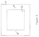
- Two such alignment marks 10 are introduced (see Fig. 3 ) into a photomask 11 at opposite sides of a circuit pattern 12 .
- the alignment marks 10 and circuit pattern 12 in the photomask 11 constitute a clear spaces in a layer of chrome on a fused silica substrate. It may be manufactured using electron-beam lithography and procured from a commercial mask shop. Two alignment marks are employed in order that angular as well as translational alignment can be accurately obtained.
- a holographic plate 13 comprising a 15 ⁇ m layer 14 of a holographic recording material spun onto a glass substrate 15 , is index-matched to a surface of a 45°, 45°, 90° prism 16 in a TIR hologram recording system.
- a suitable holographic recording material would be that identified as HRS-352 and manufactured by the company Dupont de Nemours. This material contains a monomer that polymerises an exposure to light and does not require a wet development process.
- the mask 11 is introduced into the system and positioned using piezo-electric transducers 17 so that it lies parallel to the recording layer 14 with a gap of 100 ⁇ m between it and the layer surface. Gap measurement is best achieved interferometrically by illuminating the gap with laser beams introduced via the vertical face of the prism 16 and analysing the interference of the light reflected from the surfaces of the holographic layer 14 and mask 11 .
- the technique described in EP-A-02421645 is particularly suitable.
- the laser beams need to be of a wavelength at which the holographic recording material is not sensitive. The apparatus for doing this is not shown in Fig. 3 since it is not intrinsic to the invention and could be readily formulated by someone knowledgeable in the art.
- the 100 ⁇ m gap and parallelism could alternatively be achieved by resting the mask 11 on 100 ⁇ m thick spacers laid on the surface of the recording layer 14 .
- the hologram-forming beams 18 and 19 are derived from an argon ion laser 20 operating at a wavelength of 363.8nm.
- the output of the laser 20 is divided by a beam splitter 21 into an object beam 18 and a reference beam 19 .
- the object beam 18 is reflected from a couple of mirrors 22 and passes through a beam expander 23 to illuminate the mask 11 at normal incidence.
- the reference beam 19 passes through another beam expander 24 , is reflected by a mirror 25 and enters the hypotenuse face of the prism 16 to illuminate the holographic recording layer 14 at 45°, an angle at which the beam 19 is totally internally reflected from the layer surface.
- the alignment marks 10 in the mask 11 are transferred to the holographic layer 14 as follows.
- the circuit pattern 12 in the mask 11 is covered by an opaque plate 27 and a beamblock 28 is introduced into the optical path of the reference beam 19 .
- the shutter 26 is then opened, thereby exposing the marks 10 in the mask 11 to the object beam 18 .
- the light transmitted by the alignment marks 10 polymerises the recording layer 14 , changing its refractive index and causing a localised shrinkage of the layer 14 .
- the arms 8 of the chevron features must be sufficiently wide.
- a suitable width for the arms 8 would be 6 ⁇ m.
- the beam 18 performing mark transfer be derived from the same laser 20 as used for hologram formation. It may instead be derived from, for instance, a mercury lamp. In this case an additional set of optics would be required in the recording system to direct the light from the second source onto the marks 10 in the mask 11 .
- recording of the TIR hologram proceeds. First the opaque plate 27 and the beamblock 28 are removed from the system. To prevent contamination of the recorded alignment marks by the TIR exposure the recorded marks may be shielded from the TIR exposure by appropriately blocking parts of the object and reference beams 18 and 19 (this precaution is not essential). The shutter 26 is then opened so that the object beam 18 illuminates the mask 11 and the reference beam 19 illuminates the holographic layer 14 , forming a TIR hologram in the normal way.
- a further possible procedure is to record the alignment marks simultaneously with the TIR hologram.
- those part of the recording layer 14 to receive the alignment marks have to be shielded from the reference beam 19 in order for the recorded alignment marks to have reasonable contrast.
- the recording layer 14 is then fixed by exposing it to incoherent ultraviolet radiation.
- the holographic plate 13 is then ready to be employed in a TIR holographic lithographic system.
Landscapes
- Physics & Mathematics (AREA)
- General Physics & Mathematics (AREA)
- Holo Graphy (AREA)
- Exposure Of Semiconductors, Excluding Electron Or Ion Beam Exposure (AREA)
- Exposure And Positioning Against Photoresist Photosensitive Materials (AREA)
Applications Claiming Priority (2)
| Application Number | Priority Date | Filing Date | Title |
|---|---|---|---|
| US85202492A | 1992-03-16 | 1992-03-16 | |
| US852024 | 1992-03-16 |
Publications (2)
| Publication Number | Publication Date |
|---|---|
| EP0561302A1 true EP0561302A1 (de) | 1993-09-22 |
| EP0561302B1 EP0561302B1 (de) | 1998-11-18 |
Family
ID=25312322
Family Applications (1)
| Application Number | Title | Priority Date | Filing Date |
|---|---|---|---|
| EP93104078A Expired - Lifetime EP0561302B1 (de) | 1992-03-16 | 1993-03-12 | Herstellung von Ausrichtmarken für holographische Lithographie |
Country Status (4)
| Country | Link |
|---|---|
| EP (1) | EP0561302B1 (de) |
| KR (1) | KR100258265B1 (de) |
| DE (1) | DE69322115T2 (de) |
| GB (1) | GB2272535B (de) |
Cited By (4)
| Publication number | Priority date | Publication date | Assignee | Title |
|---|---|---|---|---|
| WO1996000912A3 (en) * | 1994-06-30 | 1996-05-23 | Univ North Carolina | Achromatic optical system including diffractive optical element, and method of forming same |
| US7384709B2 (en) | 2001-03-30 | 2008-06-10 | Tesa Scribos Gmbh | Lithograph with a trigger mask and method of producing digital holograms in a storage medium |
| US7445873B2 (en) | 2001-03-30 | 2008-11-04 | Tesa Scribos Gmbh | Lithograph with beam guidance and method of producing digital holograms in a storage medium |
| WO2021129970A1 (de) * | 2019-12-23 | 2021-07-01 | Robert Bosch Gmbh | Vorrichtung und verfahren zur herstellung holographischer optischer elemente |
Families Citing this family (1)
| Publication number | Priority date | Publication date | Assignee | Title |
|---|---|---|---|---|
| KR100727777B1 (ko) | 2006-03-03 | 2007-06-14 | 주식회사 대우일렉트로닉스 | 전반사를 이용한 광정보 복제방법 및 복제장치 |
Citations (1)
| Publication number | Priority date | Publication date | Assignee | Title |
|---|---|---|---|---|
| US4857425A (en) * | 1986-06-30 | 1989-08-15 | Holtronic Technologies Limited | Manufacture of integrated circuits using holographic techniques |
Family Cites Families (1)
| Publication number | Priority date | Publication date | Assignee | Title |
|---|---|---|---|---|
| GB8802333D0 (en) * | 1988-02-03 | 1988-03-02 | Holtronic Technologies Ltd | Improvements in manufacture of integrated circuits using holographic techniques |
-
1993
- 1993-03-08 GB GB9304716A patent/GB2272535B/en not_active Expired - Fee Related
- 1993-03-12 EP EP93104078A patent/EP0561302B1/de not_active Expired - Lifetime
- 1993-03-12 DE DE69322115T patent/DE69322115T2/de not_active Expired - Fee Related
- 1993-03-13 KR KR1019930003801A patent/KR100258265B1/ko not_active Expired - Fee Related
Patent Citations (1)
| Publication number | Priority date | Publication date | Assignee | Title |
|---|---|---|---|---|
| US4857425A (en) * | 1986-06-30 | 1989-08-15 | Holtronic Technologies Limited | Manufacture of integrated circuits using holographic techniques |
Non-Patent Citations (2)
| Title |
|---|
| PATENT ABSTRACTS OF JAPAN vol. 14, no. 467 (E-989)11 October 1990 & JP-A-02 192 114 ( C A N O N I N C ) 27 July 1990 * |
| PATENT ABSTRACTS OF JAPAN vol. 8, no. 163 (P-290)27 July 1984 & JP-A-59 060 462 ( F U J I T S U K K ) 6 April 1984 * |
Cited By (6)
| Publication number | Priority date | Publication date | Assignee | Title |
|---|---|---|---|---|
| WO1996000912A3 (en) * | 1994-06-30 | 1996-05-23 | Univ North Carolina | Achromatic optical system including diffractive optical element, and method of forming same |
| US5606434A (en) * | 1994-06-30 | 1997-02-25 | University Of North Carolina | Achromatic optical system including diffractive optical element |
| US7384709B2 (en) | 2001-03-30 | 2008-06-10 | Tesa Scribos Gmbh | Lithograph with a trigger mask and method of producing digital holograms in a storage medium |
| US7445873B2 (en) | 2001-03-30 | 2008-11-04 | Tesa Scribos Gmbh | Lithograph with beam guidance and method of producing digital holograms in a storage medium |
| WO2021129970A1 (de) * | 2019-12-23 | 2021-07-01 | Robert Bosch Gmbh | Vorrichtung und verfahren zur herstellung holographischer optischer elemente |
| US12455532B2 (en) | 2019-12-23 | 2025-10-28 | Robert Bosch Gmbh | Device and method for manufacturing holographic optical elements |
Also Published As
| Publication number | Publication date |
|---|---|
| GB9304716D0 (en) | 1993-04-28 |
| GB2272535B (en) | 1995-06-07 |
| KR930020241A (ko) | 1993-10-19 |
| DE69322115T2 (de) | 1999-06-24 |
| KR100258265B1 (ko) | 2000-06-01 |
| GB2272535A (en) | 1994-05-18 |
| EP0561302B1 (de) | 1998-11-18 |
| DE69322115D1 (de) | 1998-12-24 |
Similar Documents
| Publication | Publication Date | Title |
|---|---|---|
| TWI261732B (en) | Composite optical lithography method for patterning lines of significantly different widths | |
| EP0493655B1 (de) | Vorrichtung und Verfahren zur transversalen Positionsmessung für Nah-Abstand-Lithographiesysteme | |
| EP0627666B1 (de) | Vorrichtung und Verfahren zur Veränderung des Massstabs eines gedruckten Musters | |
| JPH08179493A (ja) | 光露光または転写方法および装置またはそのためのマスク | |
| US6122056A (en) | Direct phase shift measurement between interference patterns using aerial image measurement tool | |
| KR100734589B1 (ko) | 기판 테이블, 기판의 위치를 측정하는 방법, 및 리소그래피장치 | |
| EP0561302B1 (de) | Herstellung von Ausrichtmarken für holographische Lithographie | |
| JP2000021722A (ja) | 露光方法及び露光装置 | |
| EP0560310B1 (de) | Verfahren zum Herstellen von inneren Totalreflexionshologrammen hoher Qualität | |
| US6329104B1 (en) | Position alignment system for holographic lithography process | |
| KR100282810B1 (ko) | 노광방법 및 장치 | |
| JP3296296B2 (ja) | 露光方法及び露光装置 | |
| JPH05281698A (ja) | フォトマスク及びパターン転写方法 | |
| JP3984710B2 (ja) | 露光方法及び露光装置 | |
| JPH0564448B2 (de) | ||
| JP2000021718A (ja) | 露光方法及び露光装置 | |
| Clube et al. | Holographic mask aligner | |
| US20060121357A1 (en) | Large pattern printing | |
| Dändliker et al. | Non-conventional techniques for optical lithography | |
| JP3327627B2 (ja) | 露光用原板及びそれを用いた投影露光装置 | |
| KR970004421B1 (ko) | 반도체 노광장치 | |
| JP3326446B2 (ja) | 露光方法及び装置、リソグラフィ方法、マーク焼き付け装置、及びプロキシミティ露光装置 | |
| Gray et al. | The holographic mask aligner | |
| JPH04175746A (ja) | マスク、その製造方法及びそれを用いた像形成方法 | |
| JP2818391B2 (ja) | 露光装置 |
Legal Events
| Date | Code | Title | Description |
|---|---|---|---|
| PUAI | Public reference made under article 153(3) epc to a published international application that has entered the european phase |
Free format text: ORIGINAL CODE: 0009012 |
|
| AK | Designated contracting states |
Kind code of ref document: A1 Designated state(s): CH DE FR LI NL |
|
| 17P | Request for examination filed |
Effective date: 19940321 |
|
| 17Q | First examination report despatched |
Effective date: 19970526 |
|
| GRAG | Despatch of communication of intention to grant |
Free format text: ORIGINAL CODE: EPIDOS AGRA |
|
| GRAG | Despatch of communication of intention to grant |
Free format text: ORIGINAL CODE: EPIDOS AGRA |
|
| GRAH | Despatch of communication of intention to grant a patent |
Free format text: ORIGINAL CODE: EPIDOS IGRA |
|
| GRAH | Despatch of communication of intention to grant a patent |
Free format text: ORIGINAL CODE: EPIDOS IGRA |
|
| GRAA | (expected) grant |
Free format text: ORIGINAL CODE: 0009210 |
|
| AK | Designated contracting states |
Kind code of ref document: B1 Designated state(s): CH DE FR LI NL |
|
| REG | Reference to a national code |
Ref country code: CH Ref legal event code: EP |
|
| REF | Corresponds to: |
Ref document number: 69322115 Country of ref document: DE Date of ref document: 19981224 |
|
| ET | Fr: translation filed | ||
| RAP2 | Party data changed (patent owner data changed or rights of a patent transferred) |
Owner name: HOLTRONIC TECHNOLOGIES PLC |
|
| REG | Reference to a national code |
Ref country code: CH Ref legal event code: NV Representative=s name: RIEDERER HASLER & PARTNER PATENTANWAELTE AG |
|
| NLT2 | Nl: modifications (of names), taken from the european patent patent bulletin |
Owner name: HOLTRONIC TECHNOLOGIES PLC |
|
| PLBE | No opposition filed within time limit |
Free format text: ORIGINAL CODE: 0009261 |
|
| 26N | No opposition filed | ||
| PGFP | Annual fee paid to national office [announced via postgrant information from national office to epo] |
Ref country code: FR Payment date: 20000927 Year of fee payment: 8 |
|
| PGFP | Annual fee paid to national office [announced via postgrant information from national office to epo] |
Ref country code: CH Payment date: 20000928 Year of fee payment: 8 |
|
| PGFP | Annual fee paid to national office [announced via postgrant information from national office to epo] |
Ref country code: NL Payment date: 20000930 Year of fee payment: 9 |
|
| PG25 | Lapsed in a contracting state [announced via postgrant information from national office to epo] |
Ref country code: LI Free format text: LAPSE BECAUSE OF NON-PAYMENT OF DUE FEES Effective date: 20010331 Ref country code: CH Free format text: LAPSE BECAUSE OF NON-PAYMENT OF DUE FEES Effective date: 20010331 |
|
| REG | Reference to a national code |
Ref country code: CH Ref legal event code: PL |
|
| PG25 | Lapsed in a contracting state [announced via postgrant information from national office to epo] |
Ref country code: FR Free format text: LAPSE BECAUSE OF NON-PAYMENT OF DUE FEES Effective date: 20011130 |
|
| REG | Reference to a national code |
Ref country code: FR Ref legal event code: ST |
|
| PGFP | Annual fee paid to national office [announced via postgrant information from national office to epo] |
Ref country code: DE Payment date: 20020925 Year of fee payment: 10 |
|
| PG25 | Lapsed in a contracting state [announced via postgrant information from national office to epo] |
Ref country code: NL Free format text: LAPSE BECAUSE OF NON-PAYMENT OF DUE FEES Effective date: 20021001 |
|
| NLV4 | Nl: lapsed or anulled due to non-payment of the annual fee |
Effective date: 20021001 |
|
| PG25 | Lapsed in a contracting state [announced via postgrant information from national office to epo] |
Ref country code: DE Free format text: LAPSE BECAUSE OF NON-PAYMENT OF DUE FEES Effective date: 20031001 |