EP0562880B1 - Dispositif semi-conducteur avec une face latérale oblique par rapport au clivage et son procédé de fabrication - Google Patents
Dispositif semi-conducteur avec une face latérale oblique par rapport au clivage et son procédé de fabrication Download PDFInfo
- Publication number
- EP0562880B1 EP0562880B1 EP93302378A EP93302378A EP0562880B1 EP 0562880 B1 EP0562880 B1 EP 0562880B1 EP 93302378 A EP93302378 A EP 93302378A EP 93302378 A EP93302378 A EP 93302378A EP 0562880 B1 EP0562880 B1 EP 0562880B1
- Authority
- EP
- European Patent Office
- Prior art keywords
- film
- gallium arsenide
- substrate
- infrared emitting
- emitting device
- Prior art date
- Legal status (The legal status is an assumption and is not a legal conclusion. Google has not performed a legal analysis and makes no representation as to the accuracy of the status listed.)
- Expired - Lifetime
Links
- 239000004065 semiconductor Substances 0.000 title claims description 94
- 238000000034 method Methods 0.000 title claims description 42
- 238000003776 cleavage reaction Methods 0.000 title claims description 24
- 230000007017 scission Effects 0.000 title claims description 24
- 238000004519 manufacturing process Methods 0.000 title description 7
- JBRZTFJDHDCESZ-UHFFFAOYSA-N AsGa Chemical compound [As]#[Ga] JBRZTFJDHDCESZ-UHFFFAOYSA-N 0.000 claims description 89
- 229910001218 Gallium arsenide Inorganic materials 0.000 claims description 89
- 239000000758 substrate Substances 0.000 claims description 47
- 150000001875 compounds Chemical class 0.000 claims description 16
- 230000007423 decrease Effects 0.000 claims description 8
- 230000005855 radiation Effects 0.000 claims 1
- 229910001297 Zn alloy Inorganic materials 0.000 description 10
- SAOPTAQUONRHEV-UHFFFAOYSA-N gold zinc Chemical compound [Zn].[Au] SAOPTAQUONRHEV-UHFFFAOYSA-N 0.000 description 10
- 229910052710 silicon Inorganic materials 0.000 description 9
- 239000010703 silicon Substances 0.000 description 9
- 239000012535 impurity Substances 0.000 description 8
- BYDQGSVXQDOSJJ-UHFFFAOYSA-N [Ge].[Au] Chemical compound [Ge].[Au] BYDQGSVXQDOSJJ-UHFFFAOYSA-N 0.000 description 6
- 229910000927 Ge alloy Inorganic materials 0.000 description 5
- 238000010521 absorption reaction Methods 0.000 description 5
- 239000002019 doping agent Substances 0.000 description 4
- 238000005530 etching Methods 0.000 description 4
- 239000007791 liquid phase Substances 0.000 description 4
- 239000013078 crystal Substances 0.000 description 3
- 239000007788 liquid Substances 0.000 description 3
- 238000002360 preparation method Methods 0.000 description 3
- 238000000926 separation method Methods 0.000 description 3
- 239000000853 adhesive Substances 0.000 description 2
- 230000001070 adhesive effect Effects 0.000 description 2
- FTWRSWRBSVXQPI-UHFFFAOYSA-N alumanylidynearsane;gallanylidynearsane Chemical compound [As]#[Al].[As]#[Ga] FTWRSWRBSVXQPI-UHFFFAOYSA-N 0.000 description 2
- 230000015572 biosynthetic process Effects 0.000 description 2
- 230000008021 deposition Effects 0.000 description 2
- 229920002120 photoresistant polymer Polymers 0.000 description 2
- 238000010583 slow cooling Methods 0.000 description 2
- 239000003795 chemical substances by application Substances 0.000 description 1
- 238000012986 modification Methods 0.000 description 1
- 230000004048 modification Effects 0.000 description 1
- 238000000059 patterning Methods 0.000 description 1
- 230000001105 regulatory effect Effects 0.000 description 1
- 238000012827 research and development Methods 0.000 description 1
- 238000005096 rolling process Methods 0.000 description 1
Images



Classifications
-
- H—ELECTRICITY
- H10—SEMICONDUCTOR DEVICES; ELECTRIC SOLID-STATE DEVICES NOT OTHERWISE PROVIDED FOR
- H10H—INORGANIC LIGHT-EMITTING SEMICONDUCTOR DEVICES HAVING POTENTIAL BARRIERS
- H10H20/00—Individual inorganic light-emitting semiconductor devices having potential barriers, e.g. light-emitting diodes [LED]
- H10H20/80—Constructional details
- H10H20/81—Bodies
- H10H20/819—Bodies characterised by their shape, e.g. curved or truncated substrates
-
- H—ELECTRICITY
- H10—SEMICONDUCTOR DEVICES; ELECTRIC SOLID-STATE DEVICES NOT OTHERWISE PROVIDED FOR
- H10H—INORGANIC LIGHT-EMITTING SEMICONDUCTOR DEVICES HAVING POTENTIAL BARRIERS
- H10H20/00—Individual inorganic light-emitting semiconductor devices having potential barriers, e.g. light-emitting diodes [LED]
- H10H20/01—Manufacture or treatment
Definitions
- This invention relates to a semiconductor infrared emitting device and, more particularly, to a structure of a high-power high-efficiency semiconductor infrared emitting device and process of fabricating the structure.
- the semiconductor infrared emitting device finds a wide variety of application such as an indicator incorporated in a remote control system and a part of a photo-coupler, and research and development efforts are made on high efficiency semiconductor infrared emitting device and a simple process sequence for fabrication thereof.
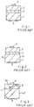
- FIG. 1 A typical example of the semiconductor infrared emitting device is illustrated in Fig. 1.
- the prior art semiconductor infrared emitting device is fabricated on an n-type gallium arsenide substrate 1 with orientation of (100), and an n-type gallium arsenide film 2 doped with silicon is grown on the major surface of the n-type gallium arsenide substrate 1.
- the n-type gallium arsenide film 2 is overlain by a p-type gallium arsenide film 3 also doped with silicon, and an electrode 4 of gold-zinc alloy is patterned on the p-type gallium arsenide film 3.
- the p-type gallium arsenide film 3 is about 50 microns to 60 microns in thickness. Electrodes 5 of gold-zinc alloy are arranged in dotted pattern on the reverse surface of the gallium arsenide substrate 1, and the dotted pattern aims at enhancement of output efficiency through reflection on the reverse surface.
- the prior art semiconductor infrared emitting device is fabricated through a process sequence described hereinbelow.
- the process sequence starts with preparation of an n-type gallium arsenide wafer serving as the n-type gallium arsenide substrates 1, and the n-type gallium arsenide layer 2 and the p-type gallium arsenide layer are sequentially grown on the n-type gallium arsenide substrate 1 through a single liquid phase epitaxial process. This is because of the fact that silicon is an amphoteric impurity, and such a single epitaxial growth is desirable in view of both cost reduction and high quality.
- the gold-zinc alloy films are patterned into the electrodes 4 and 5.
- the n-type gallium arsenide wafer is separated into the semiconductor infrared emitting devices through a dicing stage, and each of the semiconductor infrared emitting devices is shaped into a dice.
- Fig. 2 illustrates another prior art semiconductor infrared emitting device
- the second prior art semiconductor infrared emitting device is similar in structure to the first prior art semiconductor infrared emitting device except for a separation stage from the gallium arsenide wafer.
- films and electrodes are labeled with the same references designating the corresponding films and electrodes of the first prior art semiconductor infrared emitting device.
- the fabrication process for the second semiconductor infrared emitting device traces the epitaxial growing stage, the deposition stage and the patterning stage of the process sequence for the first semiconductor infrared emitting device.
- the orientation flat of the wafer or the direction of cleavage is taken into account of, and the electrodes 4 are elongated in parallel thereto.
- the separation stage is different from that of the first prior art semiconductor infrared emitting device. Namely, while dicing the gallium arsenide wafer, the gallium arsenide wafer is partially cut, and the individual semiconductor infrared emitting devices are still contiguous to one another through a half or a third of the thickness.
- Reference numeral 6 designates the cleavage surfaces which take place after the separation through the rolling stage.
- the cleavage surfaces are of the mirror surface.
- the p-type gallium arsenide layer 3 has the dopant concentration around 10 19 cm -3 , and the peak wavelength of the infrared ranges between 940 nm to 950 nm.
- the absorption coefficient is not less than 100 cm -1 with respect to the core of the wavelength, and almost half of the infrared is absorbed in the p-type gallium arsenide layer 3 of 50 to 60 microns thick.
- the n-type gallium arsenide layer 2 has the absorption coefficient ranging between 10 cm -1 to 20 cm -1 .
- the refractive index of gallium arsenide is about 3.6, and the critical angle is only 17 degrees.
- the dice-shaped prior art semiconductor infrared emitting devices tends to keep the regularity of incidental angle and reflection angle. For this reason, the infrared IR1 produced in the vicinity of the p-n junction 7 repeats reflection as shown in Fig. 3, and most of the infrared IR1 is absorbed by the p-type gallium arsenide layer 3 with the large absorption coefficient.
- another prior art semiconductor infrared emitting device has a p-type aluminum gallium arsenide layer on the p-type gallium arsenide layer 3.
- the p-type aluminum gallium arsenide layer is not so effective for the high luminous efficiency, and fairly increases the production cost. Therefore, the third prior art semiconductor infrared emitting device is less attractive.
- JP-A-62173773 discloses a light emitting diode in which first and second P-type epitaxial layers and an N-type epitaxial layer are formed on a P-type substrate.
- the substrate is selectively removed by etching to form an oblique surface, the space thus formed forming a fully reflecting surface in a boundary of the first P-type layer to improve the light emitting efficiency of the device.
- JP-A-60074642 discloses a method of separating semiconductor devices from a wafer in which a shallow groove with a large width is first formed in the wafer, with a deep groove with a smaller width being subsequently formed within this first, large groove. Thereafter, the wafer is broken and separated into each element chip.
- the present invention proposes to form a side surface of a substrate obliquely extending with respect to a cleavage surface.
- the invention provides a semiconductor infrared emitting device comprising:
- said substrate is formed of a first compound semiconductor, said substrate having a reverse surface and a top surface substantially parallel to said reverse surface;
- a preferred process for fabricating a semiconductor infrared emitting device comprises :
- Another preferred process of fabricating a semiconductor infrared emitting device comprises the steps of:
- a further preferred process of fabricating a semiconductor infrared emitting device comprises the steps of:
- a process of fabricating a semiconductor infrared emitting device comprising the steps of: a) preparing a wafer of first compound semiconductor having one conductivity type and an orientation flat surface and a vertical cleavage surface; b) successively growing a first film of the one conductivity type and a second film of the opposite conductivity type on a major surface of the wafer so that the major surface of the wafer is covered with the first film which in turn is overlain by the second film, the wafer, the first film and the second film forming in combination a multi-layer structure; c) forming upper electrodes and lower electrodes on a top surface of said second film and a reverse surface of said wafer, said upper electrodes being arranged in rows and columns;
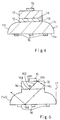
- a semiconductor infrared emitting device embodying the present invention is fabricated on an n-type gallium arsenide substrate 11 with orientation of (100), and the n-type gallium arsenide substrate 11 is shaped into a generally frusto-conical configuration.
- the n-type gallium arsenide substrate 11 has a reverse surface 11a larger in area than a major surface 11b thereof, and a curved side surface 11c is merged thereinto like a flared skirt.
- the curved side surface 11c is one and half times larger in area than the side surface of the first prior art semiconductor infrared emitting device.
- n-type gallium arsenide layer 12 is formed on the major surface 11b, and is overlain by a p-type gallium arsenide layer 13. Both n-type and p-type gallium arsenide layers 12 and 13 are doped with silicon, and a p-n junction 14 is formed along the boundary between the n-type gallium arsenide layer 12 and the p-type gallium arsenide layer 13.
- the oblique side surface 11c is wider than a vertical surface merged into a major surface and a reverse surface of a cubic substrate, and such an oblique side surface 11c is desirable for the infrared emitting device, because the area of the side surface 11c is one point seven times larger than that of the prior art.
- An electrode 15 of gold-zinc alloy is formed on the p-type gallium arsenide layer 13, and other electrodes 16 of gold-germanium are formed on the reverse surface 11a in a dotted pattern.
- the semiconductor infrared emitting device thus arranged behave as follows. If an appropriate bias voltage is applied between the electrode 15 and the electrodes 16, infrared IR2 is generated around the p-n junction. The infrared IR2 is assumed to upwardly and rightwardly proceed from a point 14a. The infrared IR2 is multiply reflected and traces a path indicated by arrows AR1. However, the infrared IR2 is taken out from the semiconductor infrared emitting device after three total reflections at 14b, 14c and 14d.
- the first prior art semiconductor infrared device absorbs the infrared IR1 after the five total reflections
- the frusto-conical gallium arsenide substrate 11 effectively takes out the infrared IR2, and, accordingly, enhances the luminous efficiency.
- a semiconductor infrared emitting device is shaped into a rectangular parallelopiped configuration such as a cube, the incident angles is theoretically equal at every crystal boundary, and infrared repeats the total reflection. This results in that most of the infrared IR1 is absorbed without radiating therefrom due to the large absorption coefficient of gallium arsenide.
- the oblique side surface 11c to the crystal boundary allows the infrared to be taken out from the semiconductor infrared emitting device.
- the side surface 11c is larger in area than a virtual surface parallel to the cleavage surface 17 in so far as one of the peripheries of the upper and reverse surfaces 11b and 11a is larger than the other of the peripheries.
- the side surface 11c contains an area declining from the cleavage surface 17 at greater than zero degrees or less than 90 degrees, the side surface 11c is effective against the absorption, and the amount of the infrared IR2 taken out therefrom is effectively increased.
- the area may decline from the cleavage surface at an angle greater than -90 degrees and less than zero.
- the amount of the infrared IR1 and the amount of the infrared IR2 were measured.
- An appropriate infrared-detector (not shown) was faced to the semiconductor infrared emitting device according to the present invention, the infrared-detector converted the infrared IR2 radiated therefrom into current, and the amount of current was proportional to the amount of infrared. While the forward bias voltage was increased from zero to 100 mA, the amount of current or the amount of the infrared IR2 traced plots PT1 as shown in Fig. 6.
- the infrared detector increased the amount of current as shown in plots PT2. Comparing the plots PT1 with the plots PT2, the amount of the infrared IR2 is one and half times larger than the amount of the infrared IR1.
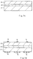
- the semiconductor infrared emitting device shown in Fig. 4 is fabricated through a process sequence, and description is hereinbefore made on the process sequence with reference to Figs. 7A to 7D.
- the process sequence starts with preparation of an n-type gallium arsenide wafer 21 having orientation of (100).
- An n-type gallium arsenide layer 22 and a p-type gallium arsenide layer 23 are successively grown through a liquid-phase slow-cooling epitaxial technique using liquid gallium arsenide doped with silicon.
- the silicon is one of amphoteric impurities, and serves as donor impurities for the n-type gallium arsenide layer 22 and as acceptor impurities for the p-type gallium arsenide layer 23.
- the resultant multi-layer structure of this stage is illustrated in Fig. 7A.
- gold-zinc alloy is selectively grown on the top surface of the p-type gallium arsenide layer through an appropriate mask, and gold-germanium alloy is also selectively grown on the reverse surface of the n-type gallium arsenide wafer 21 through another appropriate mask.
- Pieces of gold-zinc alloy serve as the upper electrodes 15, and pieces of gold-germanium alloy serve as the lower electrodes 16.
- the upper electrodes 15 are arranged in rows and columns. The resultant multi-layer structure of this stage is illustrated in Fig. 7B.
- a shallow and wide moat 24a is formed in the multilayer structure, and project from the top surface of the p-type gallium arsenide layer 23 into the n-type gallium arsenide wafer 21 through a dicing technique.
- a deep and narrow moat 24b is formed in the n-type gallium arsenide wafer 21, and project from the bottom surfaces partially defining the shallow and wide moat also through a dicing technique.
- the deep and narrow moat 24b is nested within the shallow and wide moat 24a.
- the dicing stage is repeated for forming a deep and narrow moat 24c, and the moat 24c is nested within the moat 24b.
- a deeper and narrower moat is nested within a shallower and wider moat, and the multiple moat structure 24 extends between a plurality of semiconductor infrared emitting devices arranged in rows and columns, and separates the n-type and p-type gallium arsenide layers 12 and 13 of a semiconductor infrared emitting device from the n-type and p-type gallium arsenide layers 12 and 13 of another semiconductor infrared emitting device as shown in Fig. 7C.
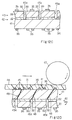
- An adhesive flexible film 25 is bonded to the reverse surface of the n-type gallium arsenide wafer 21, and a roller 26 exerts force on the n-type gallium arsenide substrate 21. Then, the n-type gallium arsenide wafer 21 is broken into the n-type gallium arsenide substrates 11, and the n-type gallium arsenide substrates 11 are shaped into generally frusto-conical configuration.
- the process sequence described hereinbefore forms the multiple moat structure 24 through dicing stages.
- a lithographic technique followed by an etching stage is available for the multiple moat structure 24. Namely, after the formation of the upper and lower electrodes 15 and 16, a photoresist mask 27a is patterned on the p-type gallium arsenide layer 23 through the lithographic technique, and the p-type gallium arsenide layer 23, the n-type gallium arsenide layer 22 and the n-type gallium arsenide substrate 21 are partially removed by using an appropriate etchant. Then, the shallow and wide moat 24a takes place in the multi-layer structure as shown in Fig. 8A.
- a photoresist mask 27b allows the etchant to form the deep and narrow moat 24c as shown in Fig. 8B.
- the moats 24a, 24b and 24c are sequentially nested with one another, and the multiple moat structure 24 is formed through the lithographic technique followed by the etching. After the formation of the multiple moat structure, the multi-layer structure is separated into a plurality of semiconductor infrared emitting devices as similar to that shown in Fig. 7D.
- FIG. 9 of the drawings another semiconductor infrared emitting device embodying the present invention is fabricated on an n-type gallium arsenide substrate 31 with orientation of (100), and the n-type gallium arsenide substrate 11 has a reverse surface 31a, a major surface 31b substantially parallel to the reverse surface 31a, and side surfaces 31c and 31d extending in parallel to each other and declining from the reverse surface 31a.
- n-type gallium arsenide layer 32 is formed on the major surface 31b, and is overlain by a p-type gallium arsenide layer 33. Both n-type and p-type gallium arsenide layers 12 and 13 are doped with silicon, and a p-n junction 34 is formed along the boundary between the n-type gallium arsenide layer 32 and the p-type gallium arsenide layer 33.
- An upper electrode 35 of gold-zinc alloy is formed on the p-type gallium arsenide layer 33, and lower electrodes 36 of gold-germanium alloy are formed on the reverse surface 31a in a dotted pattern.
- the side surfaces 31c and 31d decline from the cleavage surface CLV of an n-type gallium arsenide wafer with orientation of (100), and the angle AG between the cleavage surface CLV and the side surface 31d is regulated to an angle greater than -90 degrees and less than 90 degrees. Since the oblique side surfaces 31c and 31d are larger in area than a vertical side surface such as the vertical side surface of 6 of the prior art structure shown in Fig. 2, the semiconductor infrared emitting device shown in Fig. 9 allows the infrared produced therein to be radiated at higher probability, and, accordingly, is improved in luminous efficiency. If the side surface 31d ranges from 5 degrees to 85 degrees or -85 degrees to -5 degrees, the luminous efficiency is effectively increased.
- the semiconductor infrared emitting device thus arranged behave as follows. If an appropriate bias voltage is applied between the electrode 35 and the electrodes 36, infrared IR3 is generated around the p-n junction 34. The infrared IR3 is assumed to upwardly and rightwardly proceed from a point 34a. The infrared IR3 is multiply reflected and traces a path indicated by arrows AR2. However, the infrared IR3 is taken out from the semiconductor infrared emitting device after three total reflections at 34b, 34c and 34d.
- the arsenide substrate 31 effectively takes out the infrared IR3, and, accordingly, enhances the luminous efficiency. This is because of the fact that the total surface area of the n-type gallium arsenide substrate 31 is increased than a cubic shaped substrate.
- the amount of the infrared IR3 was measured as similar to the first embodiment. Namely, an appropriate infrared-detector (not shown) was faced to the semiconductor infrared emitting device shown in Fig. 9, the infrared-detector converted the infrared IR3 radiated therefrom into current, and the amount of current was proportional to the amount of infrared. While the forward bias voltage was increased from zero to 100 mA, the amount of current or the amount of the infrared IR3 traced plots PT3 as shown in Fig. 11. The amount of the infrared IR1 is also plotted in Fig.
- the plots PT1 stands for the amount of infrared produced in not only the first prior art semiconductor infrared emitting device shown in Fig. 1 but also the second prior art semiconductor infrared emitting device shown in Fig. 2. Comparing the plots PT1 with the plots PT3, the amount of the infrared IR3 is one point three times larger than the amount of the infrared IR1.
- the second embodiment is less effective rather than the first embodiment in view of the luminous efficiency. However, the fabrication process for the second embodiment is simpler than that of the first embodiment as described hereinbelow, and is desirable in view of productivity.
- the semiconductor infrared emitting device shown in Fig. 9 is fabricated through a process sequence, and description is hereinbefore made on the process sequence with reference to Figs. 12A to 12D.
- the process sequence starts with preparation of an n-type gallium arsenide wafer 41 having orientation of (100).
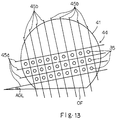
- the orientation flat surface is labeled with "OF" in Fig. 13, and is substantially vertical to the reverse surface of the n-type gallium arsenide wafer 41.
- An n-type gallium arsenide layer 42 and a p-type gallium arsenide layer 43 are successively grown through a liquid-phase slow-cooling epitaxial technique using liquid gallium arsenide doped with silicon.
- the silicon is one of amphoteric impurities, and serves as donor impurities for the n-type gallium arsenide layer 42 and as acceptor impurities for the p-type gallium arsenide layer 43.
- the resultant multi-layer structure of this stage is illustrated in Fig. 12A.
- gold-zinc alloy is selectively grown on the top surface of the p-type gallium arsenide layer, and gold-germanium alloy is also selectively grown on the reverse surface of the n-type gallium arsenide wafer 41.
- the upper electrodes 35 and the lower electrodes 36 are formed from the gold-zinc alloy film and the gold-germanium alloy film on the top surface of the p-type gallium arsenide layer 43 and the reverse surface of the n-type gallium arsenide wafer 41.
- the upper electrodes 35 are arranged in rows and columns so as to form an array 44 as shown in Fig. 13, and the rows of upper electrodes decline from the orientation flat surface OF at 10 degrees.
- the angle AGL between the rows and the orientation flat surface OF may range from 5 degrees to 85 degrees.
- Grooves are formed in the multi-layer structure by using a dicing technique, and real lines 45a and 45b are indicative of the longitudinal directions of the grooves.
- the grooves 45a extend between the rows of upper electrodes in parallel thereto, and the grooves 45b cross the grooves 45a at right angle as will be seen from Fig. 13.
- the grooves 45a and 45b are as deep as a half of the total thickness of the multi-layer structure.
- the resultant multi-layer structure is illustrated in Fig. 12C.
- An adhesive flexible film 46 is bonded to the reverse surface of the n-type gallium arsenide wafer 21, and a roller 47 travels along the grooves 45a and 45b. Force is exerted on the n-type gallium arsenide substrate 41. Then, cracks 48 take place from the grooves to the reverse surface of the wafer 41, and the n-type gallium arsenide wafer 41 is broken into the n-type gallium arsenide substrates 31.
- the cracks 48 are oblique due to the grooves 45a obliquely extending with respect to the orientation flat surface OF, and the side surfaces of the substrates 31 decline from the cleavage surface.
- compound semiconductor is not limited to gallium arsenide, and an etchant may be applied to the multiple moat structure formed through the dicing stages for creating smooth surfaces.
Landscapes
- Led Devices (AREA)
Claims (12)
- Dispositif à semi-conducteurs émettant dans l'infrarouge comportant :a) un substrat (11 ; 31) formé d'un semi-conducteur composé et ayant une surface de clivage verticale (17 ; CLV) perpendiculaire à la surface supérieure du substrat et des surfaces latérales (11c ; 31c/31d), etb) une structure multicouche (12/13 ; 32/33) formée sur ledit substrat, et agissant pour produire un rayonnement infrarouge lorsqu'une tension de polarisation est appliquée,caractérisé en ce que
lesdites surfaces latérales (11c ; 31c/31d) dudit substrat s'inclinent à l'oblique à partir de ladite surface de clivage verticale (17 ; CLV) avec un angle de valeur prédéterminée. - Dispositif selon la revendication 1, dans lequel ledit substrat est formé d'un premier semi-conducteur composé, ledit substrat ayant aussi une surface opposée (11a ; 31a) à peu près parallèle à ladite surface supérieure (11b ; 31b),ladite structure multicouche comportant un premier film (12 ; 32) d'un premier type de conductivité, formé d'un deuxième semi-conducteur composé et disposé sur ladite surface supérieure dudit substrat, et un second film (13 ; 33) d'un type de conductivité opposé, formé d'un troisième semi-conducteur composé et disposé sur ledit premier film pour former une jonction p-n entre eux (14 ; 34),ledit dispositif comportant en outreune première électrode (15 ; 35) formée sur ledit second film, etune seconde électrode (16 ; 36) formée sur ladite surface opposée dudit substrat.
- Dispositif selon la revendication 2, dans lequel lesdits premier, deuxième et troisième semi-conducteurs composés sont de l'arséniure de gallium.
- Dispositif selon l'une quelconque des revendications précédentes, dans lequel on fait varier ledit angle de valeur prédéterminée à partir de ladite surface de clivage verticale, de telle sorte que lesdites surfaces latérales ne soient pas plates.
- Dispositif selon l'une quelconque des revendications 1 à 3, dans lequel lesdites surfaces latérales sont à peu près plates.
- Dispositif selon l'une quelconque des revendications 1 à 5, dans lequel la valeur dudit angle prédéterminé est supérieure à zéro et inférieure à 90 degrés.
- Dispositif selon la revendication 6, dans lequel la valeur dudit angle prédéterminé varie entre 5 degrés et 85 degrés.
- Dispositif selon la revendication 7, dans lequel ledit angle prédéterminé est de l'ordre de 10 degrés.
- Procédé pour fabriquer un dispositif à semi-conducteurs émettant dans l'infrarouge, comportant les étapes consistant à :a) préparer une pastille (41) d'un premier semi-conducteur composé ayant un premier type de conductivité et une surface plate d'orientation (OF) et une surface de clivage verticale,b) faire croître successivement un premier film (32) ayant ledit premier type de conductivité et un second film (33) ayant le type de conductivité opposé sur une surface principale de ladite pastille, de sorte que ladite surface principale de ladite pastille soit recouverte par ledit premier film qui est à son tour recouvert par ledit second film, ledit premier film et ledit second film formant combinés l'un à l'autre une structure multicouche,c) former des électrodes supérieures (35) et des électrodes inférieures (36) sur une surface supérieure dudit second film et sur une surface opposée de ladite pastille, lesdites électrodes supérieures étant agencées en lignes et en colonnes,d) former un fossé (45a/45b) creusé vers l'intérieur à partir de ladite surface supérieure dudit second film de manière à ce qu'il passe entre lesdites lignes d'électrodes supérieures et entre lesdites colonnes d'électrodes supérieures, ete) séparer ladite structure multicouche en une pluralité de dispositifs à semi-conducteurs émettant dans l'infrarouge le long dudit fossé,caractérisé en ce que
lesdites rangées d'électrodes supérieures s'étendent à l'oblique par rapport à ladite surface plate d'orientation avec un premier angle prédéterminé de sorte que, en séparant ladite structure multicouche en une pluralité de dispositifs à semi-conducteurs émettant dans l'infrarouge le long dudit fossé, des surfaces latérales soient formées dans la pastille, celles-ci s'inclinant à l'oblique par rapport à la surface de clivage verticale avec un second angle prédéterminé. - Procédé selon la revendication 9, dans lequel ledit premier angle prédéterminé varie de 5 degrés à 85 degrés.
- Procédé selon la revendication 8, dans lequel ledit premier angle prédéterminé est de l'ordre de 10 degrés.
- Procédé selon l'une quelconque des revendications 9 à 11, dans lequel la profondeur du fossé est de l'ordre de la moitié de l'épaisseur totale de ladite structure multicouche.
Applications Claiming Priority (2)
| Application Number | Priority Date | Filing Date | Title |
|---|---|---|---|
| JP6785592 | 1992-03-26 | ||
| JP67855/92 | 1992-03-26 |
Publications (2)
| Publication Number | Publication Date |
|---|---|
| EP0562880A1 EP0562880A1 (fr) | 1993-09-29 |
| EP0562880B1 true EP0562880B1 (fr) | 1997-07-23 |
Family
ID=13356986
Family Applications (1)
| Application Number | Title | Priority Date | Filing Date |
|---|---|---|---|
| EP93302378A Expired - Lifetime EP0562880B1 (fr) | 1992-03-26 | 1993-03-26 | Dispositif semi-conducteur avec une face latérale oblique par rapport au clivage et son procédé de fabrication |
Country Status (3)
| Country | Link |
|---|---|
| US (1) | US5349211A (fr) |
| EP (1) | EP0562880B1 (fr) |
| DE (1) | DE69312360T2 (fr) |
Families Citing this family (28)
| Publication number | Priority date | Publication date | Assignee | Title |
|---|---|---|---|---|
| DE19536438A1 (de) * | 1995-09-29 | 1997-04-03 | Siemens Ag | Halbleiterbauelement und Herstellverfahren |
| US5705834A (en) * | 1996-04-23 | 1998-01-06 | The United States Of America As Represented By The Administrator Of The National Aeronautics And Space Administration | Increased efficiency LED |
| EP2315277A3 (fr) | 1998-07-28 | 2018-01-10 | Philips Lighting Holding B.V. | Dispositifs pour l'émission haute efficacité de radiations |
| US7253445B2 (en) * | 1998-07-28 | 2007-08-07 | Paul Heremans | High-efficiency radiating device |
| US6504180B1 (en) | 1998-07-28 | 2003-01-07 | Imec Vzw And Vrije Universiteit | Method of manufacturing surface textured high-efficiency radiating devices and devices obtained therefrom |
| TW502458B (en) | 1999-06-09 | 2002-09-11 | Toshiba Corp | Bonding type semiconductor substrate, semiconductor light emission element and manufacturing method thereof |
| US7205578B2 (en) * | 2000-02-15 | 2007-04-17 | Osram Gmbh | Semiconductor component which emits radiation, and method for producing the same |
| DE10006738C2 (de) * | 2000-02-15 | 2002-01-17 | Osram Opto Semiconductors Gmbh | Lichtemittierendes Bauelement mit verbesserter Lichtauskopplung und Verfahren zu seiner Herstellung |
| WO2001073859A1 (fr) * | 2000-03-24 | 2001-10-04 | Nova Crystals, Inc. | Diode electroluminescente a rendement ameliore et procede de fabrication de la diode |
| DE10019665A1 (de) * | 2000-04-19 | 2001-10-31 | Osram Opto Semiconductors Gmbh | Lumineszenzdiodenchip und Verfahren zu dessen Herstellung |
| DE20111659U1 (de) * | 2000-05-23 | 2001-12-13 | OSRAM Opto Semiconductors GmbH & Co. oHG, 93049 Regensburg | Bauelement für die Optoelektronik |
| ATE463462T1 (de) | 2000-10-09 | 2010-04-15 | Imec | Verfahren zur herstellung von mikrobearbeiteten anordnungen |
| EP1195352A1 (fr) * | 2000-10-09 | 2002-04-10 | Interuniversitair Micro-Elektronica Centrum | Procédé de fabrication de composants micro-usinés et composants ainsi fabriqués |
| DE10054966A1 (de) * | 2000-11-06 | 2002-05-16 | Osram Opto Semiconductors Gmbh | Bauelement für die Optoelektronik |
| US7078319B2 (en) * | 2000-11-17 | 2006-07-18 | Gelcore Llc | Laser separated die with tapered sidewalls for improved light extraction |
| US6791119B2 (en) * | 2001-02-01 | 2004-09-14 | Cree, Inc. | Light emitting diodes including modifications for light extraction |
| JP2003022987A (ja) | 2001-07-09 | 2003-01-24 | Sanyo Electric Co Ltd | 化合物半導体装置の製造方法 |
| DE10139798B9 (de) * | 2001-08-14 | 2006-12-28 | Osram Opto Semiconductors Gmbh | Strahlungsemittierendes Bauelement mit geometrisch optimierter Auskoppelstruktur |
| TWI236772B (en) * | 2002-03-14 | 2005-07-21 | Toshiba Corp | Semiconductor light emitting element and semiconductor light emitting device |
| JP3705791B2 (ja) * | 2002-03-14 | 2005-10-12 | 株式会社東芝 | 半導体発光素子および半導体発光装置 |
| JP3874701B2 (ja) * | 2002-06-26 | 2007-01-31 | 株式会社東芝 | 半導体発光素子及び半導体発光装置 |
| FR2878185B1 (fr) | 2004-11-22 | 2008-11-07 | Sidel Sas | Procede de fabrication de recipients comprenant une etape de chauffe au moyen d'un faisceau de rayonnement electromagnetique coherent |
| US10687391B2 (en) * | 2004-12-03 | 2020-06-16 | Pressco Ip Llc | Method and system for digital narrowband, wavelength specific cooking, curing, food preparation, and processing |
| US7425296B2 (en) * | 2004-12-03 | 2008-09-16 | Pressco Technology Inc. | Method and system for wavelength specific thermal irradiation and treatment |
| US10857722B2 (en) | 2004-12-03 | 2020-12-08 | Pressco Ip Llc | Method and system for laser-based, wavelength specific infrared irradiation treatment |
| FR2913210B1 (fr) | 2007-03-02 | 2009-05-29 | Sidel Participations | Perfectionnements a la chauffe des matieres plastiques par rayonnement infrarouge |
| JP2008235521A (ja) | 2007-03-20 | 2008-10-02 | Sanyo Electric Co Ltd | 半導体基板の割断方法及び太陽電池の割断方法並びに太陽電池 |
| FR2917005B1 (fr) | 2007-06-11 | 2009-08-28 | Sidel Participations | Installation de chauffage des corps de preformes pour le soufflage de recipients |
Family Cites Families (10)
| Publication number | Priority date | Publication date | Assignee | Title |
|---|---|---|---|---|
| US3812516A (en) * | 1970-05-01 | 1974-05-21 | Bell Telephone Labor Inc | Spontaneously emitting hetero-structure junction diodes |
| US4037241A (en) * | 1975-10-02 | 1977-07-19 | Texas Instruments Incorporated | Shaped emitters with buried-junction structure |
| JPS5380989A (en) * | 1976-12-27 | 1978-07-17 | Nippon Telegr & Teleph Corp <Ntt> | Light emitting diode |
| JPS5932073B2 (ja) * | 1979-06-01 | 1984-08-06 | 三菱電機株式会社 | 発光ダイオ−ドおよびその製造方法 |
| JPS5840872A (ja) * | 1981-09-03 | 1983-03-09 | Nec Corp | 半導体発光素子 |
| JPS5856372A (ja) * | 1981-09-29 | 1983-04-04 | Sanyo Electric Co Ltd | 発光ダイオ−ド |
| JPS61252674A (ja) * | 1985-05-01 | 1986-11-10 | Toshiba Corp | 発光ダイオ−ド |
| JPS625674A (ja) * | 1985-07-01 | 1987-01-12 | Nec Corp | 半導体発光ダイオ−ド |
| US5055894A (en) * | 1988-09-29 | 1991-10-08 | The Boeing Company | Monolithic interleaved LED/PIN photodetector array |
| EP0405757A3 (en) * | 1989-06-27 | 1991-01-30 | Hewlett-Packard Company | High efficiency light-emitting diode |
-
1993
- 1993-03-24 US US08/036,232 patent/US5349211A/en not_active Expired - Fee Related
- 1993-03-26 EP EP93302378A patent/EP0562880B1/fr not_active Expired - Lifetime
- 1993-03-26 DE DE69312360T patent/DE69312360T2/de not_active Expired - Fee Related
Also Published As
| Publication number | Publication date |
|---|---|
| DE69312360T2 (de) | 1997-11-20 |
| US5349211A (en) | 1994-09-20 |
| DE69312360D1 (de) | 1997-08-28 |
| EP0562880A1 (fr) | 1993-09-29 |
Similar Documents
| Publication | Publication Date | Title |
|---|---|---|
| EP0562880B1 (fr) | Dispositif semi-conducteur avec une face latérale oblique par rapport au clivage et son procédé de fabrication | |
| USRE38072E1 (en) | Fabrication method for AlGaInNPAsSb based devices | |
| US6323063B2 (en) | Forming LED having angled sides for increased side light extraction | |
| US6613461B1 (en) | Gallium nitride-based compound semiconductor chip and method for producing the same, and gallium nitride-based compound semiconductor wafer | |
| US5429954A (en) | Radiation-emitting diode with improved radiation output | |
| EP0580104B1 (fr) | Laser à semi-conducteur | |
| EP0666602B1 (fr) | Procédé de fabrication d'une cellule solaire en GaAs sur un substrat Si | |
| US20100295017A1 (en) | Light emitting diode element and method for fabricating the same | |
| JP3188522B2 (ja) | 発光ダイオードの形成方法 | |
| WO2003034560A1 (fr) | Procede pour produire un element electroluminescent semi-conducteur, element electroluminescent semi-conducteur, procede pour produire un element semi-conducteur, element semi-conducteur, procede pour produire un element et element | |
| KR101645738B1 (ko) | 반도체 발광 다이오드 및 반도체 발광 다이오드의 제조 방법 | |
| US5101246A (en) | Photo-functional device | |
| JP4311173B2 (ja) | 半導体発光素子 | |
| US4950622A (en) | Method for manufacturing a surface emitting type AlGaAs/GaAs semiconductor laser diode | |
| US20030119218A1 (en) | Light emitting device and manufacturing method thereof | |
| JPS6222553B2 (fr) | ||
| JPH0677522A (ja) | 発光・受光素子及びそれらの製造方法 | |
| JPH06151955A (ja) | 半導体発光素子 | |
| KR20020060617A (ko) | 질화물계 반도체칩 및 그 제조방법 | |
| JPH11354837A (ja) | 発光ダイオードおよびその製造方法 | |
| JPH03268360A (ja) | 半導体装置 | |
| JPH11168239A (ja) | 窒化ガリウム系化合物半導体発光素子 | |
| JPH06105796B2 (ja) | 発光ダイオードおよびその製造方法 | |
| KR970003850B1 (ko) | 고효율 발광소자 | |
| JPH01161782A (ja) | 発光ダイオード |
Legal Events
| Date | Code | Title | Description |
|---|---|---|---|
| PUAI | Public reference made under article 153(3) epc to a published international application that has entered the european phase |
Free format text: ORIGINAL CODE: 0009012 |
|
| AK | Designated contracting states |
Kind code of ref document: A1 Designated state(s): DE FR GB |
|
| 17P | Request for examination filed |
Effective date: 19930819 |
|
| 17Q | First examination report despatched |
Effective date: 19950223 |
|
| GRAG | Despatch of communication of intention to grant |
Free format text: ORIGINAL CODE: EPIDOS AGRA |
|
| GRAH | Despatch of communication of intention to grant a patent |
Free format text: ORIGINAL CODE: EPIDOS IGRA |
|
| GRAH | Despatch of communication of intention to grant a patent |
Free format text: ORIGINAL CODE: EPIDOS IGRA |
|
| GRAA | (expected) grant |
Free format text: ORIGINAL CODE: 0009210 |
|
| AK | Designated contracting states |
Kind code of ref document: B1 Designated state(s): DE FR GB |
|
| REF | Corresponds to: |
Ref document number: 69312360 Country of ref document: DE Date of ref document: 19970828 |
|
| ET | Fr: translation filed | ||
| PLBE | No opposition filed within time limit |
Free format text: ORIGINAL CODE: 0009261 |
|
| STAA | Information on the status of an ep patent application or granted ep patent |
Free format text: STATUS: NO OPPOSITION FILED WITHIN TIME LIMIT |
|
| 26N | No opposition filed | ||
| REG | Reference to a national code |
Ref country code: GB Ref legal event code: IF02 |
|
| REG | Reference to a national code |
Ref country code: GB Ref legal event code: 732E |
|
| REG | Reference to a national code |
Ref country code: FR Ref legal event code: TP |
|
| PGFP | Annual fee paid to national office [announced via postgrant information from national office to epo] |
Ref country code: FR Payment date: 20050308 Year of fee payment: 13 |
|
| PGFP | Annual fee paid to national office [announced via postgrant information from national office to epo] |
Ref country code: GB Payment date: 20050323 Year of fee payment: 13 |
|
| PGFP | Annual fee paid to national office [announced via postgrant information from national office to epo] |
Ref country code: DE Payment date: 20050324 Year of fee payment: 13 |
|
| PG25 | Lapsed in a contracting state [announced via postgrant information from national office to epo] |
Ref country code: GB Free format text: LAPSE BECAUSE OF NON-PAYMENT OF DUE FEES Effective date: 20060326 |
|
| PG25 | Lapsed in a contracting state [announced via postgrant information from national office to epo] |
Ref country code: DE Free format text: LAPSE BECAUSE OF NON-PAYMENT OF DUE FEES Effective date: 20061003 |
|
| GBPC | Gb: european patent ceased through non-payment of renewal fee |
Effective date: 20060326 |
|
| REG | Reference to a national code |
Ref country code: FR Ref legal event code: ST Effective date: 20061130 |
|
| PG25 | Lapsed in a contracting state [announced via postgrant information from national office to epo] |
Ref country code: FR Free format text: LAPSE BECAUSE OF NON-PAYMENT OF DUE FEES Effective date: 20060331 |