EP0566997A1 - Plasmaadressierte elektrooptische Vorrichtung - Google Patents
Plasmaadressierte elektrooptische Vorrichtung Download PDFInfo
- Publication number
- EP0566997A1 EP0566997A1 EP93106169A EP93106169A EP0566997A1 EP 0566997 A1 EP0566997 A1 EP 0566997A1 EP 93106169 A EP93106169 A EP 93106169A EP 93106169 A EP93106169 A EP 93106169A EP 0566997 A1 EP0566997 A1 EP 0566997A1
- Authority
- EP
- European Patent Office
- Prior art keywords
- plasma
- substrate
- discharge
- electro
- electrodes
- Prior art date
- Legal status (The legal status is an assumption and is not a legal conclusion. Google has not performed a legal analysis and makes no representation as to the accuracy of the status listed.)
- Granted
Links
Images


Classifications
-
- G—PHYSICS
- G02—OPTICS
- G02F—OPTICAL DEVICES OR ARRANGEMENTS FOR THE CONTROL OF LIGHT BY MODIFICATION OF THE OPTICAL PROPERTIES OF THE MEDIA OF THE ELEMENTS INVOLVED THEREIN; NON-LINEAR OPTICS; FREQUENCY-CHANGING OF LIGHT; OPTICAL LOGIC ELEMENTS; OPTICAL ANALOGUE/DIGITAL CONVERTERS
- G02F1/00—Devices or arrangements for the control of the intensity, colour, phase, polarisation or direction of light arriving from an independent light source, e.g. switching, gating or modulating; Non-linear optics
- G02F1/01—Devices or arrangements for the control of the intensity, colour, phase, polarisation or direction of light arriving from an independent light source, e.g. switching, gating or modulating; Non-linear optics for the control of the intensity, phase, polarisation or colour
- G02F1/13—Devices or arrangements for the control of the intensity, colour, phase, polarisation or direction of light arriving from an independent light source, e.g. switching, gating or modulating; Non-linear optics for the control of the intensity, phase, polarisation or colour based on liquid crystals, e.g. single liquid crystal display cells
- G02F1/133—Constructional arrangements; Operation of liquid crystal cells; Circuit arrangements
- G02F1/1333—Constructional arrangements; Manufacturing methods
- G02F1/13334—Plasma addressed liquid crystal cells [PALC]
-
- G—PHYSICS
- G02—OPTICS
- G02F—OPTICAL DEVICES OR ARRANGEMENTS FOR THE CONTROL OF LIGHT BY MODIFICATION OF THE OPTICAL PROPERTIES OF THE MEDIA OF THE ELEMENTS INVOLVED THEREIN; NON-LINEAR OPTICS; FREQUENCY-CHANGING OF LIGHT; OPTICAL LOGIC ELEMENTS; OPTICAL ANALOGUE/DIGITAL CONVERTERS
- G02F1/00—Devices or arrangements for the control of the intensity, colour, phase, polarisation or direction of light arriving from an independent light source, e.g. switching, gating or modulating; Non-linear optics
- G02F1/01—Devices or arrangements for the control of the intensity, colour, phase, polarisation or direction of light arriving from an independent light source, e.g. switching, gating or modulating; Non-linear optics for the control of the intensity, phase, polarisation or colour
- G02F1/13—Devices or arrangements for the control of the intensity, colour, phase, polarisation or direction of light arriving from an independent light source, e.g. switching, gating or modulating; Non-linear optics for the control of the intensity, phase, polarisation or colour based on liquid crystals, e.g. single liquid crystal display cells
- G02F1/133—Constructional arrangements; Operation of liquid crystal cells; Circuit arrangements
- G02F1/1333—Constructional arrangements; Manufacturing methods
- G02F1/133374—Constructional arrangements; Manufacturing methods for displaying permanent signs or marks
Definitions
- the present invention relates to a plasma addressing electro-optical device having a dual-layer structure constituted of an electro-optical cell such as a liquid crystal cell and a plasma cell, and more particularly to a structure of the plasma cell.
- an active matrix addressing system is generally known as means for effecting a high resolution and a high contrast.
- a plurality of switching elements such as thin film transistors are individually provided for a plurality of picture elements, and the switching elements are driven in a line sequential manner.
- semiconductor elements such as thin film transistors must be provided on a substrate, there occurs a problem such that an yield is reduced particularly in the case of enlarging a picture area of the device.
- Japanese Patent Laid-open Publication No. 1-217396 corresponding to U.S. Patents No. 4,896,149 and No. 5,077,553
- a system of utilizing plasma switches rather than the switching elements such as thin film transistors.
- the conventional plasma addressing electro-optical device has a laminated flat panel structure constituted of a liquid crystal cell 101, a plasma cell 102 and an intermediate plate 103 interposed between the liquid crystal cell 101 and the plasma cell 102.
- the plasma cell 102 is formed from a glass substrate 104.
- a plurality of parallel grooves 105 are formed on an upper surface of the glass substrate 104.
- the grooves 105 extend in a direction of rows of a matrix, for example.
- the grooves 105 are enclosed by the intermediate plate 103 to thereby define a plurality of individual plasma chambers 106.
- An ionizable gas is sealed in each of the plasma chambers 106.
- a crest portion 107 formed between adjacent ones of the grooves 105 serves as a barrier rib for separating the plasma chambers 106 from each other and as a gap spacer for the plasma chambers 106.
- a pair of plasma electrodes 108 and 109 extending in parallel to each other are provided on a bottom portion of each groove 105.
- the pair of plasma electrodes 108 and 109 function as an anode A and a cathode K for ionizing the gas in each plasma chamber 106 to generate a discharge plasma.
- a discharge region between the anode A and the cathode K serves as a line scanning unit.
- the bottom portion of each groove 105 is formed as a curved surface, and the pair of anode A and cathode K are disposed on the curved surface to incline with respect to each other at a predetermined angle in opposed relationship to each other. Accordingly, plasma discharge easily occurs between an electrode surface of the anode A and an electrode surface of the cathode K.
- the liquid crystal cell 101 is constructed of a transparent substrate 110 and a liquid crystal layer 111 formed between the transparent substrate 110 and the intermediate plate 103.
- the transparent substrate 110 is opposed to the intermediate plate 103 with a predetermined space defined therebetween, and the liquid crystal layer 111 is filled in this space.
- a plurality of signal electrodes 112 are formed on an inside or lower surface of the transparent substrate 110 so as to extend in perpendicular relationship to the plasma chambers 106, thereby forming column driving units.
- the signal electrodes 112 are formed of a transparent conductive material. Accordingly, a plurality of picture elements are arranged in a matrix form at the intersections between the column driving units of the liquid crystal cell 101 and the line scanning units of the plasma cell 102.
- the plasma chambers 106 of the plasma cell 102 are selectively scanned in a line sequential manner, and in synchronism therewith an analog driving voltage is applied to the signal electrodes 112 of the liquid crystal cell 101, thereby effecting display driving.
- an anode potential is reached almost over each plasma chamber 106 to select the picture elements every line. That is, the plasma chambers 106 function as sampling switches.
- a driving voltage is applied to each picture element under the condition where the plasma sampling switches are ON, sampling and holding are performed to control an on or off state of each picture element. Even after the plasma sampling switches become OFF, the analog driving voltage is held in each picture element as it is.
- the above electro-optical device utilizing the discharge plasma may have an advantage such that a picture area of the device can be enlarged more easily than that in an electro-optical device using semiconductor elements.
- various problems remain in practical application.
- the formation of the grooves 105 defining the plasma chambers 106 on the substrate 104 such as a glass substrate is considerably difficult in manufacturing.
- the plasma electrodes 108 and 109 for discharging are necessarily formed in each groove 105, an etching process for forming the plasma electrodes 108 and 109 is troublesome.
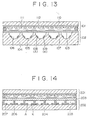
- this improved device also has a laminated flat panel structure constituted of a liquid crystal cell 201 and a plasma cell 202.
- the liquid crystal cell 201 has the basically same structure as that of the liquid crystal cell 101 shown in Fig. 13.
- the plasma cell 202 is constituted of an intermediate plate 203 and a lower substrate 204 opposed to each other with a predetermined space defined therebetween. This space is partitioned by a plurality of barrier ribs 206 to define a plurality of plasma chambers 205. Each plasma chamber 205 forms a discharge region as a line scanning unit. An ionizable gas is sealed in each plasma chamber 205.
- the barrier ribs 206 are formed by a printing process.
- a pair of plasma electrodes 207 are formed in each separate discharge region to serve as an anode A and a cathode K.
- the plasma electrodes 207 are formed on an upper flat surface of the substrate 204 by a printing process. As the printing process is a very simple technique, the productivity and the workability can be improved as compared with those in forming the grooves in the related art. Further, the printing process is fit for enlargement of a picture area.
- the plasma cell is of a surface discharge type such that plasma discharge occurs between the upper surface of the anode and the upper surface of the cathode.
- the upper surfaces of the anode and the cathode are of the same level, and they are not opposed to each other.
- the upper surfaces of the anode and the cathode shown in Fig. 13 are opposed to each other at a given inclined angle. In this manner, the electrode surfaces of the plasma cell shown in Fig. 14 are not opposed to each other In spite of the surface discharge type, thus possibly causing the above discharge defect.
- a plasma addressing electro-optical device comprising a first substrate having a major surface; a plurality of first electrodes formed on said major surface of said first substrate so as to extend in substantially parallel relationship to each other; a second substrate having a major surface opposed to said major surface of said first substrate; a plurality of second electrodes formed on said major surface of said second substrate so as to extend in substantially parallel relationship to each other to generate plasma addressing between adjacent ones of said second electrodes; an electro-optical material layer formed between said first substrate and said second substrate; and a plasma discharge chamber formed between said electro-optical material layer and said second substrate so as to seal an ionizable gas therein, said plasma discharge chamber having a height of about 75 % or more of a distance between said adjacent ones of said second electrodes.
- An arcuate path of plasma discharge is formed between an upper surface of an anode and an upper surface of a cathode disposed on the same level in the plasma chamber.
- a negative charge such as electrons and a positive charge such as ions contained in the plasma are allowed to move along the arcuate path.
- the height of the plasma chamber that is, the space of the plasma cell is defined to some degree to thereby ensure the discharge path, thus maintaining stable and uniform plasma discharge.
- the condition for realizing the stable and uniform plasma discharge is to set the height of the plasma chamber to about 75 % or more of the distance between the anode and the cathode adjacent to each other. If the height is smaller than this value, the discharge path will be blocked to result in a disadvantage that an effective discharge region cannot be formed.
- the height of the plasma chamber in the plasma addressing electro-optical device is set to about 75 % or more of the distance between the anode and the cathode adjacent to each other, thereby obtaining stable and uniform plasma discharge. Accordingly, the line-sequential operation of the plasma addressing electro-optical device with the discharge region functioning as a scanning unit can be reliably performed.
- FIG. 1 there is shown a schematic fragmentary sectional view of a basic structure of a plasma addressing display device according to the preferred embodiment.
- the sectional view of Fig. 1 is taken along a column direction, that is, a longitudinal direction of signal electrodes 5 to be hereinafter described.
- the display device shown in Fig. 1 has a flat panel structure formed by laminating a liquid crystal cell 1, a plasma cell 2 and an intermediate plate 3 as a dielectric material layer interposed between the liquid crystal cell 1 and the plasma cell 2.
- the liquid crystal cell 1 is comprised of a glass substrate 4 opposed to the intermediate plate 3 with a predetermined space defined therebetween, a plurality of signal electrodes 5 formed on a lower or major surface of the glass substrate 4 so as to extend in parallel to each other in the column direction, and a liquid crystal layer 6 formed so as to fill the space defined between the glass substrate 4 and the intermediate plate 3.
- the signal electrodes 5 are formed from a transparent conductive film, and the liquid crystal layer 6 is formed of an electro-optical material. While the present invention is applied to the plasma addressing display device in this preferred embodiment, it is not limited to this preferred embodiment but may be widely applied to a plasma addressing electro-optical device such as an optical modulating device.
- the plasma cell 2 is comprised of a glass substrate 7 opposed to the intermediate plate 3 with a sealed plasma chamber 9 defined therebetween, and a plurality of plasma electrodes 8 formed on an upper or major surface of the glass substrate 7 so as to extend in parallel to each other in a line direction perpendicular to the column direction, that is, perpendicular to the longitudinal direction of the signal electrodes 5. Adjacent ones of the plasma electrodes 8 function alternately as an anode A and a cathode K spaced a predetermined distance d.
- the sealed plasma chamber 9 has a predetermined height h, and contains an ionizable gas selected from He, Ne, Ar, or a mixture thereof.
- the structure of the plasma cell in the present invention is not limited to such an open cell structure but it may be a structure having barrier ribs as shown in Fig. 14.
- the space between the intermediate plate 3 and the glass substrate 7, that is, the height h of the plasma chamber 9 is set to be 75 % or more of the distance d between the anode A and the cathode K adjacent to each other.
- a plasma discharge path between the anode A and the cathode K shows an arc or parabola.
- a peak of the parabola increases in proportion to the interelectrode distance d.
- the height h of the plasma chamber 9 must be set according to the interelectrode distance d so that the parabolic discharge path may not be cut off by a ceiling portion of the plasma cell 2, that is, by the intermediate plate 3.
- the ratio of the height h to the distance d is set to about 75 % or more. If the height h is set to less than 75 % of the distance d as shown by a dotted line in Fig. 1, the plasma discharge does not effectively be generated.
- the plasma electrodes 8 are configured in a stripe pattern having a stripe length of 132 mm, a stripe width of 0.15 mm, a stripe pitch of 0.39 mm, and a stripe number of 200.
- the plasma electrodes 8 are formed by printing or vapor deposition with use of a metal material such as Ni or Ag.
- the ionizable gas sealed in the plasma chamber 9 is Ne containing 0.5 % of Ar.
- a discharge voltage is applied to the plasma cell 9 by DC scanning or DC static driving.
- the wedge-shaped cell As shown in Fig. 2, the wedge-shaped cell is generally constructed of a pair of glass substrates 21 and 22 laminated to each other at one end thereof and a spacer 23 interposed therebetween at the other end, thereby defining a wedge-shaped plasma chamber 25 having a height h continuously changed.
- a plurality of plasma electrodes 24 having a stripe pattern are formed on an upper or inside surface of the lower glass substrate 22 so as to be spaced an interelectrode distance d.
- the height of a transitional region where the discharge starts to become unstable will be defined as a minimum height H required for stable discharge.
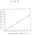
- the intermediate distance d (a minimum distance between one side of the anode and one side of the cathode opposed to the one side of the anode) was varied as a parameter to prepare three kinds of wedge-shaped cells. Then, the minimum height H was measured by using the three kinds of wedge-shaped cells. The result of measurement is shown in Fig. 3.
- the minimum height H was about 0.2 mm for a parameter d of 0.23 mm; the minimum height H was about 0.3 mm for a parameter d of 0.4 mm; and the minimum height H was about O.52 mm for a parameter of 0.74 mm.
- Fig. 3 The minimum height H was about 0.2 mm for a parameter d of 0.23 mm; the minimum height H was about 0.3 mm for a parameter d of 0.4 mm; and the minimum height H was about O.52 mm for a parameter of 0.74 mm
- the relation between the minimum height H and the interelectrode distance d is substantially proportional to each other to provide a slope of 0.75.
- the minimum height of the plasma chamber necessary for obtaining stable plasma discharge or glow discharge is about 75 % of the interelectrode distance.
- Fig. 4 shows a mechanism of discharge under the condition of a uniform electric field in general parallel flat plates.
- A an anode
- K cathode
- Electrons are collected on the surface of the anode to show a negative space charge
- positive ions are collected on the surface of the cathode to show a positive space charge.
- a potential distribution in the space between the anode and the cathode is shown by a curve in Fig. 4.
- a positive space charge effect is greater than a negative space charge effect is that the positive ion is larger in weight than the electron to show a moving velocity lower than that of the electron and stay longer in the space than the electron.
- Fig. 5 shows an extremely approximated representation of the potential distribution shown in Fig. 4.
- the plasma is present in a space between M and A, so that this space can be considered as a conductor. Accordingly, it can be considered that the anode A is advanced to the position M. This is equivalent to that the interelectrode distance d has been reduced to d0. According to such a consideration, the generation of a space charge by discharge can provide an effect similar to that to be provided by a reduction in the interelectrode distance.
- the product pd0 of the gas pressure p and the interelectrode distance d0 will be hereinafter referred to as "equivalent pd" for convenience.
- the Paschen's law (the law of relation between the product pd and a discharge starting voltage V s ) will now be examined in consideration of the above.
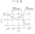
- pd > (pd) min a voltage V D for maintaining continuous discharge after starting of discharge decreases from the discharge starting voltage V s with an increase in discharge current to show a negative resistance characteristic as shown by a solid line V s - b in Fig. 7. Accordingly, when no load resistance is present, a total resistance of a circuit becomes negative.
- V D - I characteristic becomes a negative resistance characteristic as shown by a dotted line y - z in Fig. 7, and breakdown occurs as similar to the case of V s -b.
- a maximum value of V D appearing in such a course is called a breakdown voltage V B .
- V B > V s is shown in the case of pd ⁇ (pd) min
- V s V B is shown in the case of pd > (pd) min .
- the phenomenon of the breakdown is apparently visible.
- V -I characteristic the discharge voltage - current characteristic
- the form of the potential distribution as shown in Fig. 4 is decided by a current density i rather than a total current I. Accordingly, when the current density i becomes large at a certain portion of the cathode surface because of any reason, the product pd at this portion is reduced to the "equivalent pd". That is, when there is created a region where the current density i becomes larger because of electric field concentration or the like, the discharge maintaining voltage V D in this region is reduced. As a result, the current density i in this region is further increased to cause further remarkable concentration of the current.
- V D terminates at the time when the current density i reaches a value (in) which makes the "equivalent pd" equal to (pd) min , and simultaneously the phenomenon of the current concentration is also ended.
- the total current I is defined by a load resistance.
- the voltage V D in this section between h and j is lower by one or more figures than that in the glow discharge.
- the discharge in the section between h and j is called an arc discharge.
- the above description with reference to Figs. 4 to 8 is shown in the literature "Gas Discharge” (written by Hatta; published by Kindai Kagaku-sha), for example.
- the lines of electric force in the plasma chamber do not intersect each other, and show parabolic forms.
- an electric field is nonuniform, and in principle, it is intensively collected particularly at the electrode end.
- the electrode end is remarkably nonuniform in shape.
- the lines of electric force are apt to be collected at one point of the electrode end to cause an appearance of a remarkable nonuniform electric field region.
- a uniform electric field is necessary to maintain the uniform normal glow discharge. That is, the maintenance of the uniform normal glow discharge is hindered by the remarkable nonuniform electric field.
- a discharge path that is, a path of electrons from the cathode to the anode is considered to extend generally along the lines of electric force in average from a statistic viewpoint although there is a possibility of collision between the electrons and gas atoms in the path to cause deviation of the electrons from the path.
- a distance d of the discharge path is given in the range of about 0.24 - 0.6 mm.
- the distance d corresponds to the interelectrode distance in the Paschen's law.
- a ratio of (pd) max and (pd) min becomes two times or more.
- FIG. 9 The discharge occurring in such a plasma cell as shown in Fig. 9 may be considered in the following cases.
- reference numerals 1 to 4 denote discharge path Nos., and in the following description, (pd)1 ⁇ 4 correspond to the discharge path Nos. 1 to 4, respectively.
- the normal glow discharge occurs in the discharge path No. 3.
- a current density becomes locally high because of a remarkable nonuniform electric field, and so breakdown or discharge like the arc discharge is apt to occur in this local region.
- the voltage drops to stop the discharge.
- discontinuous discharge locally occurs, and uniform and continuous discharge cannot be obtained as a whole.
- the test result shown in Fig. 3 demonstrates that the height corresponding to the normal discharge path is about 75 % of the interelectrode distance based on the electrode end in the structure shown in Fig. 1.
- the ratio of 75 % is invariable regardless of a change in the interelectrode distance.
- the above consideration is in good agreement with the phenomenon observed in the test, that is, no contradiction arises.
- the reason why the predetermined height is required is considered to depend upon the discharge path with a high possibility.
Landscapes
- Physics & Mathematics (AREA)
- Nonlinear Science (AREA)
- Engineering & Computer Science (AREA)
- Plasma & Fusion (AREA)
- Mathematical Physics (AREA)
- Chemical & Material Sciences (AREA)
- Crystallography & Structural Chemistry (AREA)
- General Physics & Mathematics (AREA)
- Optics & Photonics (AREA)
- Liquid Crystal (AREA)
- Gas-Filled Discharge Tubes (AREA)
- Devices For Indicating Variable Information By Combining Individual Elements (AREA)
Applications Claiming Priority (2)
| Application Number | Priority Date | Filing Date | Title |
|---|---|---|---|
| JP12826292A JP3161024B2 (ja) | 1992-04-21 | 1992-04-21 | プラズマアドレス電気光学装置 |
| JP128262/92 | 1992-04-21 |
Publications (2)
| Publication Number | Publication Date |
|---|---|
| EP0566997A1 true EP0566997A1 (de) | 1993-10-27 |
| EP0566997B1 EP0566997B1 (de) | 1998-06-17 |
Family
ID=14980499
Family Applications (1)
| Application Number | Title | Priority Date | Filing Date |
|---|---|---|---|
| EP93106169A Expired - Lifetime EP0566997B1 (de) | 1992-04-21 | 1993-04-15 | Plasmaadressierte elektrooptische Vorrichtung |
Country Status (5)
| Country | Link |
|---|---|
| US (1) | US5548421A (de) |
| EP (1) | EP0566997B1 (de) |
| JP (1) | JP3161024B2 (de) |
| KR (1) | KR100259930B1 (de) |
| DE (1) | DE69319172T2 (de) |
Cited By (3)
| Publication number | Priority date | Publication date | Assignee | Title |
|---|---|---|---|---|
| US5696569A (en) * | 1994-12-21 | 1997-12-09 | Philips Electronics North America | Channel configuration for plasma addressed liquid crystal display |
| AU698245B2 (en) * | 1994-06-30 | 1998-10-29 | Sony Corporation | Plasma addressed liquid crystal display apparatus |
| EP0779643B1 (de) * | 1995-12-15 | 2003-09-17 | Matsushita Electric Industrial Co., Ltd. | Plasmaanzeigetafel geeignet für Anzeige hoher Qualität |
Families Citing this family (10)
| Publication number | Priority date | Publication date | Assignee | Title |
|---|---|---|---|---|
| US5754329A (en) * | 1992-12-22 | 1998-05-19 | Monsanto Company | Electrochromic display laminates |
| US5413739A (en) * | 1992-12-22 | 1995-05-09 | Coleman; James P. | Electrochromic materials and displays |
| TW354380B (en) * | 1995-03-17 | 1999-03-11 | Hitachi Ltd | A liquid crystal device with a wide visual angle |
| JPH08286172A (ja) * | 1995-04-17 | 1996-11-01 | Sony Corp | プラズマアドレス表示装置 |
| CA2220519A1 (en) * | 1995-05-09 | 1996-11-21 | James P. Coleman | Conductive font |
| BR9609201A (pt) * | 1995-06-07 | 2001-05-15 | Monsanto Co | Dispositivo e método para modulação de luz |
| US6344883B2 (en) * | 1996-12-20 | 2002-02-05 | Sharp Kabushiki Kaisha | Liquid crystal display device and method for producing the same |
| KR100252990B1 (ko) * | 1997-10-24 | 2000-04-15 | 구자홍 | 아크 방전전극을 갖는 칼라 플라즈마 디스플레이패널 |
| JP3215866B2 (ja) | 1999-03-26 | 2001-10-09 | 名古屋大学長 | 排気ガス浄化用触媒に用いる金属製担体の製造方法 |
| KR101225645B1 (ko) * | 2012-11-12 | 2013-01-24 | 주식회사 성현기업 | 이탈방지 구조를 갖는 플러그 및 라인콘센트 |
Citations (1)
| Publication number | Priority date | Publication date | Assignee | Title |
|---|---|---|---|---|
| US4896149A (en) * | 1988-01-19 | 1990-01-23 | Tektronix, Inc. | Addressing structure using ionizable gaseous medium |
Family Cites Families (3)
| Publication number | Priority date | Publication date | Assignee | Title |
|---|---|---|---|---|
| KR940010842B1 (ko) * | 1991-10-26 | 1994-11-17 | 삼성전관 주식회사 | 플라즈마 어드레스 방식의 액정표시소자 |
| KR940006301B1 (ko) * | 1991-10-29 | 1994-07-14 | 삼성전관 주식회사 | 프라즈마 어드레스 방식의 액정표시소자와 그 제조방법 |
| KR940004290B1 (ko) * | 1991-11-27 | 1994-05-19 | 삼성전관 주식회사 | 플라즈마 어드레스 방식의 액정표시소자와 그 제조 방법 |
-
1992
- 1992-04-21 JP JP12826292A patent/JP3161024B2/ja not_active Expired - Lifetime
-
1993
- 1993-04-15 DE DE69319172T patent/DE69319172T2/de not_active Expired - Lifetime
- 1993-04-15 EP EP93106169A patent/EP0566997B1/de not_active Expired - Lifetime
- 1993-04-19 KR KR1019930006526A patent/KR100259930B1/ko not_active Expired - Lifetime
-
1995
- 1995-04-18 US US08/423,139 patent/US5548421A/en not_active Expired - Lifetime
Patent Citations (1)
| Publication number | Priority date | Publication date | Assignee | Title |
|---|---|---|---|---|
| US4896149A (en) * | 1988-01-19 | 1990-01-23 | Tektronix, Inc. | Addressing structure using ionizable gaseous medium |
Non-Patent Citations (2)
| Title |
|---|
| IEEE TRANSACTIONS ON ELECTRON DEVICES vol. 23, no. 3, March 1976, NEW YORK US pages 328 - 331 S.SATO ET AL. 'Surface-Discharge-Type Plasma Display Panel' * |
| IEEE TRANSACTIONS ON ELECTRON DEVICES vol. ED-28, no. 9, September 1981, NEW YORK US pages 1035 - 1042 M.ANANDAN ET AL. 'Coplanar Gas-Discharge Display' * |
Cited By (5)
| Publication number | Priority date | Publication date | Assignee | Title |
|---|---|---|---|---|
| AU698245B2 (en) * | 1994-06-30 | 1998-10-29 | Sony Corporation | Plasma addressed liquid crystal display apparatus |
| RU2139560C1 (ru) * | 1994-06-30 | 1999-10-10 | Сони Корпорейшн | Плазменное устройство, предназначенное для жидкокристаллического дисплея |
| US5696569A (en) * | 1994-12-21 | 1997-12-09 | Philips Electronics North America | Channel configuration for plasma addressed liquid crystal display |
| EP0779643B1 (de) * | 1995-12-15 | 2003-09-17 | Matsushita Electric Industrial Co., Ltd. | Plasmaanzeigetafel geeignet für Anzeige hoher Qualität |
| USRE41503E1 (en) | 1995-12-15 | 2010-08-17 | Panasonic Corporation | Method of producing plasma display panel with protective layer of an alkaline earth oxide |
Also Published As
| Publication number | Publication date |
|---|---|
| DE69319172T2 (de) | 1999-02-11 |
| KR930022429A (ko) | 1993-11-24 |
| KR100259930B1 (ko) | 2000-06-15 |
| EP0566997B1 (de) | 1998-06-17 |
| US5548421A (en) | 1996-08-20 |
| JP3161024B2 (ja) | 2001-04-25 |
| JPH05297360A (ja) | 1993-11-12 |
| DE69319172D1 (de) | 1998-07-23 |
Similar Documents
| Publication | Publication Date | Title |
|---|---|---|
| EP0567021B1 (de) | Plasmaadressierte elektrooptische Vorrichtung | |
| US5548421A (en) | Plasma addressing electro-optical device having electrodes on a planar surface | |
| KR100259929B1 (ko) | 플라즈마어드레싱전광장치 및 어드레싱구조 | |
| JP2654745B2 (ja) | プラズマ・アドレス装置 | |
| EP0567019B1 (de) | Plasmaadressierte elektrooptische Vorrichtung | |
| JPH04229530A (ja) | プラズマ表示素子とその製造方法 | |
| US5898271A (en) | Hollow cathodes with an I-beam or C-beam cross section for a plasma display device | |
| CN1148896A (zh) | 带有蚀刻电极的等离子体寻址液晶显示器 | |
| US5834896A (en) | Plasma display with barrier ribs | |
| EP1434250B1 (de) | Plasmaanzeigetafel | |
| EP0726485A1 (de) | Plasmaadressiert flüssigkristall-anzeigevorrichtung | |
| US5689153A (en) | Electro-optical plasma display device with electrode having insulating layers | |
| JPH0572518A (ja) | プラズマアドレス表示装置 | |
| CN1111890C (zh) | 等离子体显示装置的电极排列 | |
| JP3271084B2 (ja) | プラズマアドレス電気光学装置 | |
| KR100910896B1 (ko) | 플라즈마 디스플레이 | |
| JP3378193B2 (ja) | プラズマアドレス表示装置 | |
| US6597330B1 (en) | Plasma addressed display device | |
| JPH0862588A (ja) | プラズマ表示装置 | |
| US20030057830A1 (en) | Sputter resistant secondary emission coating for electrodes | |
| JPH10221678A (ja) | 半ac型放電スイッチを有する液晶表示装置 | |
| JPH11271724A (ja) | プラズマアドレス液晶表示装置 |
Legal Events
| Date | Code | Title | Description |
|---|---|---|---|
| PUAI | Public reference made under article 153(3) epc to a published international application that has entered the european phase |
Free format text: ORIGINAL CODE: 0009012 |
|
| AK | Designated contracting states |
Kind code of ref document: A1 Designated state(s): DE FR GB |
|
| 17P | Request for examination filed |
Effective date: 19940324 |
|
| 17Q | First examination report despatched |
Effective date: 19960109 |
|
| GRAG | Despatch of communication of intention to grant |
Free format text: ORIGINAL CODE: EPIDOS AGRA |
|
| GRAG | Despatch of communication of intention to grant |
Free format text: ORIGINAL CODE: EPIDOS AGRA |
|
| GRAH | Despatch of communication of intention to grant a patent |
Free format text: ORIGINAL CODE: EPIDOS IGRA |
|
| RAP1 | Party data changed (applicant data changed or rights of an application transferred) |
Owner name: SONY CORPORATION |
|
| GRAH | Despatch of communication of intention to grant a patent |
Free format text: ORIGINAL CODE: EPIDOS IGRA |
|
| GRAA | (expected) grant |
Free format text: ORIGINAL CODE: 0009210 |
|
| AK | Designated contracting states |
Kind code of ref document: B1 Designated state(s): DE FR GB |
|
| REF | Corresponds to: |
Ref document number: 69319172 Country of ref document: DE Date of ref document: 19980723 |
|
| ET | Fr: translation filed | ||
| PLBE | No opposition filed within time limit |
Free format text: ORIGINAL CODE: 0009261 |
|
| 26N | No opposition filed | ||
| REG | Reference to a national code |
Ref country code: GB Ref legal event code: IF02 |
|
| PGFP | Annual fee paid to national office [announced via postgrant information from national office to epo] |
Ref country code: DE Payment date: 20120420 Year of fee payment: 20 |
|
| PGFP | Annual fee paid to national office [announced via postgrant information from national office to epo] |
Ref country code: FR Payment date: 20120507 Year of fee payment: 20 Ref country code: GB Payment date: 20120419 Year of fee payment: 20 |
|
| REG | Reference to a national code |
Ref country code: DE Ref legal event code: R071 Ref document number: 69319172 Country of ref document: DE |
|
| REG | Reference to a national code |
Ref country code: GB Ref legal event code: PE20 Expiry date: 20130414 |
|
| PG25 | Lapsed in a contracting state [announced via postgrant information from national office to epo] |
Ref country code: GB Free format text: LAPSE BECAUSE OF EXPIRATION OF PROTECTION Effective date: 20130414 Ref country code: DE Free format text: LAPSE BECAUSE OF EXPIRATION OF PROTECTION Effective date: 20130416 |