EP0567111A1 - Electrode d'une élément photovoltaique et sa méthode de fabrication - Google Patents
Electrode d'une élément photovoltaique et sa méthode de fabrication Download PDFInfo
- Publication number
- EP0567111A1 EP0567111A1 EP93106540A EP93106540A EP0567111A1 EP 0567111 A1 EP0567111 A1 EP 0567111A1 EP 93106540 A EP93106540 A EP 93106540A EP 93106540 A EP93106540 A EP 93106540A EP 0567111 A1 EP0567111 A1 EP 0567111A1
- Authority
- EP
- European Patent Office
- Prior art keywords
- photovoltaic element
- type
- paste
- molecular weight
- average molecular
- Prior art date
- Legal status (The legal status is an assumption and is not a legal conclusion. Google has not performed a legal analysis and makes no representation as to the accuracy of the status listed.)
- Granted
Links
Images


Classifications
-
- H—ELECTRICITY
- H10—SEMICONDUCTOR DEVICES; ELECTRIC SOLID-STATE DEVICES NOT OTHERWISE PROVIDED FOR
- H10F—INORGANIC SEMICONDUCTOR DEVICES SENSITIVE TO INFRARED RADIATION, LIGHT, ELECTROMAGNETIC RADIATION OF SHORTER WAVELENGTH OR CORPUSCULAR RADIATION
- H10F77/00—Constructional details of devices covered by this subclass
- H10F77/20—Electrodes
- H10F77/206—Electrodes for devices having potential barriers
- H10F77/211—Electrodes for devices having potential barriers for photovoltaic cells
-
- H—ELECTRICITY
- H10—SEMICONDUCTOR DEVICES; ELECTRIC SOLID-STATE DEVICES NOT OTHERWISE PROVIDED FOR
- H10F—INORGANIC SEMICONDUCTOR DEVICES SENSITIVE TO INFRARED RADIATION, LIGHT, ELECTROMAGNETIC RADIATION OF SHORTER WAVELENGTH OR CORPUSCULAR RADIATION
- H10F71/00—Manufacture or treatment of devices covered by this subclass
-
- H—ELECTRICITY
- H10—SEMICONDUCTOR DEVICES; ELECTRIC SOLID-STATE DEVICES NOT OTHERWISE PROVIDED FOR
- H10F—INORGANIC SEMICONDUCTOR DEVICES SENSITIVE TO INFRARED RADIATION, LIGHT, ELECTROMAGNETIC RADIATION OF SHORTER WAVELENGTH OR CORPUSCULAR RADIATION
- H10F77/00—Constructional details of devices covered by this subclass
- H10F77/10—Semiconductor bodies
- H10F77/16—Material structures, e.g. crystalline structures, film structures or crystal plane orientations
- H10F77/162—Non-monocrystalline materials, e.g. semiconductor particles embedded in insulating materials
-
- Y—GENERAL TAGGING OF NEW TECHNOLOGICAL DEVELOPMENTS; GENERAL TAGGING OF CROSS-SECTIONAL TECHNOLOGIES SPANNING OVER SEVERAL SECTIONS OF THE IPC; TECHNICAL SUBJECTS COVERED BY FORMER USPC CROSS-REFERENCE ART COLLECTIONS [XRACs] AND DIGESTS
- Y02—TECHNOLOGIES OR APPLICATIONS FOR MITIGATION OR ADAPTATION AGAINST CLIMATE CHANGE
- Y02E—REDUCTION OF GREENHOUSE GAS [GHG] EMISSIONS, RELATED TO ENERGY GENERATION, TRANSMISSION OR DISTRIBUTION
- Y02E10/00—Energy generation through renewable energy sources
- Y02E10/50—Photovoltaic [PV] energy
Definitions
- the present invention relates to a semiconductor element having a collecting electrode superior in weathering proof, and particularly to a photovoltaic element which is easy to be fabricated and has a longterm reliability in water proof, as well as a forming method thereof.
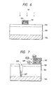
- FIG. 6 An example of a conventional solar cell is shown in Fig. 6.
- a photoelectric conversion layer 103 made of an amorphous silicone is formed on an electrically conductive substrate 104, and a transparent electrically conductive layer 102 also useful as an anti-reflection layer is formed thereon. Further, on the transparent electrically conductive layer is formed a collecting grid electrode 101 for collecting current more effectively. If light is incident on the photoelectric conversion layer 103 from the side of the collecting electrode 101, as shown in Fig. 6, light energy is converted into electric current within the photoelectric conversion layer, and taken out from the collecting electrode 101 and the electrically conductive substrate 104 as the outputs.
- the photoelectric conversion layer contains at least one or more pin junctions, with the p-side acting as an anode and the n-side as a cathode.
- solar cells having an output of several watts or greater are used outdoors. Therefore, these solar cells are required to have the durability against the temperature and humidity, or the environment proof.
- the collecting electrode when the collecting electrode is formed on the non-single crystal photovoltaic semiconductor, it must be formed in a large area at a temperature not to damage the quality of film on the semiconductor, whereby an electroconductive paste is used.
- a conventional solar cell is shown in Fig. 6.
- Fig. 6 There are a number of voids or interstices 105 of various sizes in the collecting electrode 101.
- moisture from the outside passes through the solar cell module to permeate into such voids or interstices, and dissolve electroconductive base substance such as silver contained in the collecting electrode by photovoltaic power of the solar cell itself.
- electroconductive base substance dissolved may diffuse and grow through defective portions such as pinholes of semiconductor, causing a short-circuit between the positive and negative electrodes of the solar cell, resulting in a problem of greatly decreasing the conversion efficiency.
- the electroconductive base substance is silver
- the reaction occurs between the anode and the cathode, according to the following formula, thereby giving rise to a short-circuit.
- FIG. 7 A silver ion 605 produced by the reaction between Ag 2 0 and water within the collecting electrode 101 of the anode side enters a pinhole 606 existing in the photoelectric conversion layer 103 owing to an electromotive force produced by the photovoltaic element, sticking to the electrically conductive substrate 104 to form a resinous crystal 607. If the resinous crystal 607 grows, the collecting electrode 101 and the electrically conductive substrate 104 of the solar cell are short-circuited, thereby decreasing the conversion efficiency. If the reaction further progresses, the output of solar cell can not be taken out.
- This electromigration phenomenon is not limited to silver, but can occur on copper, solder and gold.
- an object of the present invention is to provide a photovoltaic element which has high environment proof, and especially is easy to fabricate with the conversion efficiency not degrading in the permeation of water contents.
- the present invention provides a photovoltaic element having a photoelectric conversion layer and a collecting electrode formed by curing a paste having at least a conductive base substance and a curable resin on said photoelectric conversion layer, wherein the number average molecular weight of said curable resin is 3000 or less, and wherein the weight ratio of said electroconductive base substance to said collecting electrode is 70% or more, and wherein said curable resin contains at least one kind of urethan type, epoxy type, polyimide type, polyester type, phenol type, vinyl type, and acrylic type.
- the present invention provides a method for forming a photovoltaic element, wherein said curing is performed in a range from 120°C to 250°C, and wherein said electroconductive base substance is any one of silver, silver paradium alloy, a mixture of silver and carbon, copper, nickel, aluminum, and gold, and wherein said photovoltaic element is non-single crystal semiconductor, further including the steps of forming a paste having an electroconductive base substance and a curable resin having a number average molecular weight of 3000 or less on said photoelectric conversion layer, and forming a collecting electrode by curing said paste.
- moisture entering from the outside may react with electroconductive base substance such as silver, producing silver ions to give rise to a short-circuit between electrodes.
- the curable resin as the electroconductive paste may have the number average molecular weight of 3000 or less, with a greater mobility of resin, the resin extending across the collecting electrode, which makes it difficult to produce voids or interstices. Accordingly, water contents become less liable to reach the electroconductive base substance, so that it is possible to suppress the reaction of the chemical formula (A) as previously noted, and thus the creation of silver ions. As a result, it is possible to prevent the short-circuit between electrodes.
- the curable resin having a number average molecular weight of 3000 or less has a greater mobility of resin, which causes the resin to sink more or less, whereby silver ions become difficult to reach the transparent conductive layer, thereby making it possible to prevent the short-circuit.
- the present invention it is possible to provide a photovoltaic element which is unlikely to cause electromigration and has excellent environment proof. Also, since the conversion efficiency is not degraded, the total costs for the photovoltaic element can be reduced.
- Asolar cell according to the present invention is made up in the following way, when an amorphous silicone deposited on a conductive substrate is used as a photoelectric conversion semiconductor layer.
- an amorphous silicone layer having at least one or more pin junctions is formed by plasma CVD using silane gas, for example.
- the conductive substrate include stainless, aluminum, copper, titanium, carbon sheet and so on.
- the substrate may be a resin substrate having a metal deposited thereon.
- a transparent conductive layer made of indium oxide or tin oxide by vapor deposition or spraying.
- an electroconductive paste composed of an electroconductive base substance and a curable resin is applied on the transparent conductive layer by screen printing, and cured at a temperature ranging from 100 to 200°C to form a collecting electrode.
- Examples of the electroconductive base substance in the electroconductive paste include silver, silver-palladium alloy, a mixture of silver and carbon, copper, nickel, aluminum, gold and so on.
- Agrid electrode preferably contains an electroconductive base substance of at least 70 wt%, and more preferably at 75 wt% or greater, in order to obtain an electric conductivity necessary for passing the electric current.
- the curable resin include urethan type, epoxy type, polyimide type, polyester type, phenol type, vinyl type, and acrylic type, whose number average molecular weight is 3000 or less.
- the epoxy type is most preferable from the viewpoint of the waterproof and the economy. Since impurities such as chlorine or sodium contained in the electroconductive paste will act as the catalyst in the above-mentioned electromigration reaction and promote the creation of metallic ions, it is preferable to contain as least amount of impurities as possible.
- the extent of voids or interstices in the collecting electrode generally depends on the kind of resin for forming the collecting electrode, as well as the temperature and time in forming, but if a sufficient curable time is given at a temperature of 120°C or greater, the crosslinking degree of resin is not substantially changed, resulting in little change in the extent of voids or interstices.
- the forming temperature is substantially in a range from 120°C to 250°C, depending on the kind of resin. At temperature of 120°C or below, the crosslinking of the resin in the paste is so insufficient that the electrical conductivity or adhering force may be reduced, while at temperatures of 250°C or above, the film quality of amorphous semiconductor is degraded.
- the present invention will be now described in detail by way of examples.
- the number average molecular weight of the curable resin in the present invention was measured by a gel permeation chromatography (GPC).
- the gel permeation chromatography used herein is that using a property that the adsorbent can adsorb more sample having smaller molecular weight, a sample for measurement is passed through a column (like a pipe of adsorbent) which is held thermostatic, whereby the average molecular weight is determined by the adsorbed amount and the time.
- Two pin-type photoelectric conversion layers composed of an amorphous silicone were deposited on a stainless substrate having a thickness of 8MIL and an area of 16 cm 2 by plasma CVD, and a transparent conductive layer composed of indium oxide was adhered thereto by sputtering.
- an electroconductive paste composed of a urethan type resin and silver particulates (70 wt% electroconductive base substance, 20 wt% urethan type resin with a number average molecular weight of 2010, 10 wt% solvent (methyl ethyl ketone)) was screen printed into a desired shape, and cured at a temperature of 130°C for one hour to make up a solar cell of this example.
- This solar cell is referred to as a tandem type, its optimal operation voltage being 1.2 V.
- Aforward bias of 1.2 V was applied to this solar cell under the conditions of a high temperature of 85°C and a high humidity of 85%RH to appropriately measure the temporal change of leak current flowing within the solar cell.
- the forward bias was applied to simulate the operation state.
- the measurement result is indicated by the solid line A in Fig. 2.
- the axis of ordinates of Fig. 2 indicates the leak current per unit area, and the axis of abscissas indicates the time.
- a solar cell was fabricated under the same conditions as in the example 1, and the same test as above was performed.
- a solar cell was fabricated under the same conditions as in the example 1, and the same test as above was performed.
- This result is shown in Fig. 2.
- the polyimide type resin (with a number average molecular weight of 14400) is indicated by the dot-and-dash line B, while the polyester type resin (with a number average molecular weight of 31000) is indicated by the broken line C.
- the leak current of the solar cell in the comparative example has greatly increased such as 1.7 mAlcm 2 for the polyimide type per hour, and 2 mAlcm 2 per hour for the polyester type, while the solar cell in the example 1 is 0.2 mA/cm 2 per hour, which is about one-tenth that of the comparative example, indicating that the elution of silver has greatly reduced.
- a tandem-type solar cell was fabricated using a paste composed of an epoxy type resin and silver particulates (80 wt% electroconductive base substance, 20 wt% epoxy resin with a number average molecular weight of 540, solventless).
- the curing conditions were 150°C and three hours.
- a forward bias was applied to this solar cell under the conditions of a high temperature of 85°C and a high humidity of 85%RH to measure the increase amount of leak current.
- Fig. 3 the solid line D indicates the leak current in this example, while the dot-and-dash line B and the dotted line C indicate the temporal change of leak current for the polyimide type resin (with a number average molecular weight of 14400) and the polyester type resin (with a number average molecular weight of 3100) of the comparative example, respectively, as shown in Fig. 2.
- the increase amount of leak current was 0.03 mAlcm 2 per hour, which was about 1/100 that of the comparative example. This is substantially 1/10 that of the example 1, which indicates that further great effects can be expected by using an electroconductive paste composing of a resin having a smaller number average molecular weight.
- tandem-type amorphous solar cells X, Y and Z of the polyester type resin were fabricated in the same way as in the example 1, except that the number average molecular weight of unsaturated polyester type resin was 2900 for X, 3350 for Y and 5000 for Z.
- a forward bias was applied to this solar cell under the conditions of a high temperature of 85°C and a high humidity of 85%RH to measure the temporal change of leak current. This result is shown in Fig. 4.
- Fig. 4 In Fig.
- the solid line X indicates the temporal change of leak current when using a paste wherein the number average molecular weight of unsaturated polyester type resin is 2900
- the dotted line Y indicates the temporal change of leak current when using a paste wherein the number average molecular weight of unsaturated polyester type resin is 3350
- the dot-and-dash line Z indicates the temporal change of leak current when using a paste wherein the number average molecular weight of unsaturated polyester type resin is 5000.
- the increase rate of leak current is a very small value such as 0.25 mAlcm 2 when using a paste as indicated the solid line X, with a very small migration of silver, while the amount of leak current increases when using pastes of the dotted line Y and the dot-and-dash line Z which have greater molecular weights, and in particular, when using a paste of the dot-and-dash line Z, it can be found that the leak current is 1.1 mAlcm 2 , which is roughly four to five times that of a paste as indicated by the solid line X. This suggests that even though the same unsaturated polyester type resin is used, the amount of elution for silver will vary depending on the molecular weight, providing different characteristics as to migration resistance.
- the use of a collecting electrode composed of a resin having a number average molecular weight of 3000 or less makes it possible to prevent the short-circuit between electrodes of a photovoltaic element from occurring due to permeation of water contents, and to provide a solar cell which is easy to fabricate and excellent in the environment proof.
- the collecting electrode is composed of a mixture of a resin and an electroconductive base substance, the grid can be formed at low temperatures, whereby it is possible to fabricate a solar cell inexpensively.
- the grid containing a resin according to the present invention is bendable and strong against mechanical impacts, it is possible to provide a photovoltaic element which is flexible and rugged.
- a photovoltaic element has a photoelectric conversion layer and a collecting electrode formed by curing a paste having at least an electroconductive base substance and a curable resin on the photoelectric conversion layer.
- the number average molecular weight of the curable resin is 3000 or less.
Landscapes
- Photovoltaic Devices (AREA)
- Conductive Materials (AREA)
Applications Claiming Priority (2)
| Application Number | Priority Date | Filing Date | Title |
|---|---|---|---|
| JP130066/92 | 1992-04-23 | ||
| JP13006692 | 1992-04-23 |
Publications (2)
| Publication Number | Publication Date |
|---|---|
| EP0567111A1 true EP0567111A1 (fr) | 1993-10-27 |
| EP0567111B1 EP0567111B1 (fr) | 1996-07-17 |
Family
ID=15025198
Family Applications (1)
| Application Number | Title | Priority Date | Filing Date |
|---|---|---|---|
| EP93106540A Expired - Lifetime EP0567111B1 (fr) | 1992-04-23 | 1993-04-22 | Electrode d'une élément photovoltaique et sa méthode de fabrication |
Country Status (7)
| Country | Link |
|---|---|
| US (1) | US5340409A (fr) |
| EP (1) | EP0567111B1 (fr) |
| KR (1) | KR0156268B1 (fr) |
| AT (1) | ATE140561T1 (fr) |
| AU (1) | AU646773B2 (fr) |
| DE (1) | DE69303655T2 (fr) |
| ES (1) | ES2089629T3 (fr) |
Cited By (1)
| Publication number | Priority date | Publication date | Assignee | Title |
|---|---|---|---|---|
| US6214636B1 (en) * | 1992-07-15 | 2001-04-10 | Canon Kabushiki Kaisha | Photovoltaic device with improved collector electrode |
Families Citing this family (8)
| Publication number | Priority date | Publication date | Assignee | Title |
|---|---|---|---|---|
| GB9123684D0 (en) * | 1991-11-07 | 1992-01-02 | Bp Solar Ltd | Ohmic contacts |
| DE69534582T2 (de) * | 1994-05-19 | 2006-07-20 | Canon K.K. | Photovoltaisches Bauelement, Elektrodenstruktur desselben und Herstellungsverfahren |
| DE10338577A1 (de) * | 2003-08-19 | 2005-03-31 | Ekkehard Steinecke | Behälter für Schüttgut und Verfahren zur Herstellung eines Behälters für Schüttgut |
| US20050209512A1 (en) * | 2004-03-16 | 2005-09-22 | Heruth Kenneth T | Detecting sleep |
| TWI442583B (zh) * | 2006-11-28 | 2014-06-21 | Sanyo Electric Co | 太陽電池模組 |
| US8288646B2 (en) * | 2009-05-06 | 2012-10-16 | UltraSolar Technology, Inc. | Pyroelectric solar technology apparatus and method |
| JPWO2012124463A1 (ja) * | 2011-03-17 | 2014-07-17 | 三洋電機株式会社 | 太陽電池及び太陽電池モジュール |
| US20130240009A1 (en) * | 2012-03-18 | 2013-09-19 | The Boeing Company | Metal Dendrite-free Solar Cell |
Citations (2)
| Publication number | Priority date | Publication date | Assignee | Title |
|---|---|---|---|---|
| US4084985A (en) * | 1977-04-25 | 1978-04-18 | The United States Of America As Represented By The Administrator Of The National Aeronautics And Space Administration | Method for producing solar energy panels by automation |
| DE3804831C1 (en) * | 1988-02-17 | 1989-07-20 | Degussa Ag, 6000 Frankfurt, De | Electroconductive coating composition for the contacting of solar cells |
Family Cites Families (8)
| Publication number | Priority date | Publication date | Assignee | Title |
|---|---|---|---|---|
| US4293451A (en) * | 1978-06-08 | 1981-10-06 | Bernd Ross | Screenable contact structure and method for semiconductor devices |
| JPS6393164A (ja) * | 1986-10-08 | 1988-04-23 | Matsushita Electric Ind Co Ltd | 光起電力素子の製造方法 |
| JPS63185071A (ja) * | 1987-01-27 | 1988-07-30 | Matsushita Electric Ind Co Ltd | 非晶質太陽電池 |
| US4968354A (en) * | 1987-11-09 | 1990-11-06 | Fuji Electric Co., Ltd. | Thin film solar cell array |
| JPH01149484A (ja) * | 1987-12-04 | 1989-06-12 | Sanyo Electric Co Ltd | 光起電力装置 |
| JPH036867A (ja) * | 1989-06-05 | 1991-01-14 | Mitsubishi Electric Corp | 光発電素子の電極構造、形成方法、及びその製造装置 |
| JP3156973B2 (ja) * | 1991-10-18 | 2001-04-16 | キヤノン株式会社 | 太陽電池 |
| JPH1057762A (ja) * | 1996-08-21 | 1998-03-03 | Nkk Corp | 触媒の反応および再生装置ならびにその方法 |
-
1993
- 1993-04-15 US US08/046,131 patent/US5340409A/en not_active Expired - Lifetime
- 1993-04-21 AU AU37056/93A patent/AU646773B2/en not_active Ceased
- 1993-04-22 DE DE69303655T patent/DE69303655T2/de not_active Expired - Lifetime
- 1993-04-22 AT AT93106540T patent/ATE140561T1/de not_active IP Right Cessation
- 1993-04-22 ES ES93106540T patent/ES2089629T3/es not_active Expired - Lifetime
- 1993-04-22 KR KR1019930006778A patent/KR0156268B1/ko not_active Expired - Fee Related
- 1993-04-22 EP EP93106540A patent/EP0567111B1/fr not_active Expired - Lifetime
Patent Citations (2)
| Publication number | Priority date | Publication date | Assignee | Title |
|---|---|---|---|---|
| US4084985A (en) * | 1977-04-25 | 1978-04-18 | The United States Of America As Represented By The Administrator Of The National Aeronautics And Space Administration | Method for producing solar energy panels by automation |
| DE3804831C1 (en) * | 1988-02-17 | 1989-07-20 | Degussa Ag, 6000 Frankfurt, De | Electroconductive coating composition for the contacting of solar cells |
Non-Patent Citations (5)
| Title |
|---|
| PATENT ABSTRACTS OF JAPAN vol. 012, no. 330 (E-655)7 September 1988 & JP-A-63 093 164 ( MATSUSHITA ELECTRIC IND CO LTD ) 23 April 1988 * |
| PATENT ABSTRACTS OF JAPAN vol. 012, no. 461 (E-689)5 December 1988 & JP-A-63 185 071 ( MATSUSHITA ELECTRIC IND CO LTD ) 30 July 1988 * |
| PATENT ABSTRACTS OF JAPAN vol. 013, no. 264 (E-774)19 June 1989 & JP-A-01 057 762 ( KYOCERA CORP ) 6 March 1989 * |
| PATENT ABSTRACTS OF JAPAN vol. 014, no. 344 (E-955)25 July 1990 & JP-A-02 117 177 ( FUJI ELECTRIC CO LTD ) 1 May 1990 * |
| PATENT ABSTRACTS OF JAPAN vol. 015, no. 170 (E-1062)30 April 1991 & JP-A-03 038 069 ( FUJI ELECTRIC CO LTD ) 19 February 1991 * |
Cited By (1)
| Publication number | Priority date | Publication date | Assignee | Title |
|---|---|---|---|---|
| US6214636B1 (en) * | 1992-07-15 | 2001-04-10 | Canon Kabushiki Kaisha | Photovoltaic device with improved collector electrode |
Also Published As
| Publication number | Publication date |
|---|---|
| DE69303655D1 (de) | 1996-08-22 |
| KR0156268B1 (ko) | 1998-12-01 |
| ATE140561T1 (de) | 1996-08-15 |
| AU3705693A (en) | 1993-11-11 |
| AU646773B2 (en) | 1994-03-03 |
| EP0567111B1 (fr) | 1996-07-17 |
| KR930022612A (ko) | 1993-11-24 |
| DE69303655T2 (de) | 1996-12-19 |
| US5340409A (en) | 1994-08-23 |
| ES2089629T3 (es) | 1996-10-01 |
Similar Documents
| Publication | Publication Date | Title |
|---|---|---|
| US6051778A (en) | Electrode structure, process production thereof and photo-electricity generating device including the electrode | |
| US5527717A (en) | Method of making solar cell module with improved weathering characteristics | |
| US4084985A (en) | Method for producing solar energy panels by automation | |
| US5707459A (en) | Solar cell module provided with a heat-fused portion | |
| US6132585A (en) | Semiconductor element and method and apparatus for fabricating the same | |
| US5380371A (en) | Photoelectric conversion element and fabrication method thereof | |
| EP0274890B1 (fr) | Contacts ohmiques stables pour couches minces de semi-conducteurs II-VI de type p contenant du tellure | |
| US5286306A (en) | Thin film photovoltaic cells from I-III-VI-VII compounds | |
| US7141863B1 (en) | Method of making diode structures | |
| EP0537730B1 (fr) | Cellule solaire | |
| JPH0563953B2 (fr) | ||
| Albright et al. | Efficient CdTe/CdS solar cells and modules by spray processing | |
| EP0567111B1 (fr) | Electrode d'une élément photovoltaique et sa méthode de fabrication | |
| JP4266840B2 (ja) | 太陽電池モジュール | |
| JPH06318724A (ja) | 電極及び光起電力素子 | |
| JPH06318723A (ja) | 光起電力素子およびその作製方法 | |
| JP3078951B2 (ja) | 光起電力素子 | |
| US20070006913A1 (en) | Improved Photovoltaic Device and Module | |
| JPH0794767A (ja) | 光電変換素子 | |
| JPH0918040A (ja) | 集電電極および光起電力素子 | |
| Ullal et al. | Polycrystalline thin-film solar cells and modules | |
| JPH06196737A (ja) | 太陽電池 | |
| Albright et al. | High-efficiency large-area CdTe modules | |
| Burton et al. | Optimization of the CdS-Cu 2 S backwall solar cell | |
| JPH06151908A (ja) | 太陽電池の欠陥封止方法 |
Legal Events
| Date | Code | Title | Description |
|---|---|---|---|
| PUAI | Public reference made under article 153(3) epc to a published international application that has entered the european phase |
Free format text: ORIGINAL CODE: 0009012 |
|
| AK | Designated contracting states |
Kind code of ref document: A1 Designated state(s): AT BE CH DE DK ES FR GB GR IE IT LI LU MC NL PT SE |
|
| 17P | Request for examination filed |
Effective date: 19940314 |
|
| 17Q | First examination report despatched |
Effective date: 19950609 |
|
| GRAH | Despatch of communication of intention to grant a patent |
Free format text: ORIGINAL CODE: EPIDOS IGRA |
|
| ITF | It: translation for a ep patent filed | ||
| GRAA | (expected) grant |
Free format text: ORIGINAL CODE: 0009210 |
|
| AK | Designated contracting states |
Kind code of ref document: B1 Designated state(s): AT BE CH DE DK ES FR GB GR IE IT LI LU MC NL PT SE |
|
| PG25 | Lapsed in a contracting state [announced via postgrant information from national office to epo] |
Ref country code: NL Free format text: LAPSE BECAUSE OF FAILURE TO SUBMIT A TRANSLATION OF THE DESCRIPTION OR TO PAY THE FEE WITHIN THE PRESCRIBED TIME-LIMIT Effective date: 19960717 Ref country code: GR Free format text: LAPSE BECAUSE OF FAILURE TO SUBMIT A TRANSLATION OF THE DESCRIPTION OR TO PAY THE FEE WITHIN THE PRESCRIBED TIME-LIMIT Effective date: 19960717 Ref country code: DK Effective date: 19960717 Ref country code: BE Effective date: 19960717 Ref country code: AT Effective date: 19960717 |
|
| REF | Corresponds to: |
Ref document number: 140561 Country of ref document: AT Date of ref document: 19960815 Kind code of ref document: T |
|
| REG | Reference to a national code |
Ref country code: CH Ref legal event code: NV Representative=s name: BOVARD AG PATENTANWAELTE |
|
| REG | Reference to a national code |
Ref country code: IE Ref legal event code: FG4D Free format text: 69139 |
|
| REF | Corresponds to: |
Ref document number: 69303655 Country of ref document: DE Date of ref document: 19960822 |
|
| REG | Reference to a national code |
Ref country code: ES Ref legal event code: FG2A Ref document number: 2089629 Country of ref document: ES Kind code of ref document: T3 |
|
| PG25 | Lapsed in a contracting state [announced via postgrant information from national office to epo] |
Ref country code: SE Effective date: 19961017 Ref country code: PT Effective date: 19961017 |
|
| ET | Fr: translation filed | ||
| REG | Reference to a national code |
Ref country code: ES Ref legal event code: FG2A Ref document number: 2089629 Country of ref document: ES Kind code of ref document: T3 |
|
| NLV1 | Nl: lapsed or annulled due to failure to fulfill the requirements of art. 29p and 29m of the patents act | ||
| PG25 | Lapsed in a contracting state [announced via postgrant information from national office to epo] |
Ref country code: IE Free format text: LAPSE BECAUSE OF NON-PAYMENT OF DUE FEES Effective date: 19970422 |
|
| PG25 | Lapsed in a contracting state [announced via postgrant information from national office to epo] |
Ref country code: LU Free format text: LAPSE BECAUSE OF NON-PAYMENT OF DUE FEES Effective date: 19970430 |
|
| PLBE | No opposition filed within time limit |
Free format text: ORIGINAL CODE: 0009261 |
|
| 26N | No opposition filed | ||
| PG25 | Lapsed in a contracting state [announced via postgrant information from national office to epo] |
Ref country code: MC Effective date: 19971031 |
|
| REG | Reference to a national code |
Ref country code: GB Ref legal event code: IF02 |
|
| PGFP | Annual fee paid to national office [announced via postgrant information from national office to epo] |
Ref country code: FR Payment date: 20050408 Year of fee payment: 13 |
|
| PGFP | Annual fee paid to national office [announced via postgrant information from national office to epo] |
Ref country code: GB Payment date: 20050420 Year of fee payment: 13 |
|
| PGFP | Annual fee paid to national office [announced via postgrant information from national office to epo] |
Ref country code: CH Payment date: 20050427 Year of fee payment: 13 |
|
| PGFP | Annual fee paid to national office [announced via postgrant information from national office to epo] |
Ref country code: ES Payment date: 20050527 Year of fee payment: 13 |
|
| PG25 | Lapsed in a contracting state [announced via postgrant information from national office to epo] |
Ref country code: GB Free format text: LAPSE BECAUSE OF NON-PAYMENT OF DUE FEES Effective date: 20060422 |
|
| PG25 | Lapsed in a contracting state [announced via postgrant information from national office to epo] |
Ref country code: ES Free format text: LAPSE BECAUSE OF NON-PAYMENT OF DUE FEES Effective date: 20060424 |
|
| PG25 | Lapsed in a contracting state [announced via postgrant information from national office to epo] |
Ref country code: LI Free format text: LAPSE BECAUSE OF NON-PAYMENT OF DUE FEES Effective date: 20060430 Ref country code: CH Free format text: LAPSE BECAUSE OF NON-PAYMENT OF DUE FEES Effective date: 20060430 |
|
| PGFP | Annual fee paid to national office [announced via postgrant information from national office to epo] |
Ref country code: IT Payment date: 20060430 Year of fee payment: 14 |
|
| REG | Reference to a national code |
Ref country code: CH Ref legal event code: PL |
|
| GBPC | Gb: european patent ceased through non-payment of renewal fee |
Effective date: 20060422 |
|
| REG | Reference to a national code |
Ref country code: FR Ref legal event code: ST Effective date: 20061230 |
|
| REG | Reference to a national code |
Ref country code: ES Ref legal event code: FD2A Effective date: 20060424 |
|
| PG25 | Lapsed in a contracting state [announced via postgrant information from national office to epo] |
Ref country code: FR Free format text: LAPSE BECAUSE OF NON-PAYMENT OF DUE FEES Effective date: 20060502 |
|
| PG25 | Lapsed in a contracting state [announced via postgrant information from national office to epo] |
Ref country code: IT Free format text: LAPSE BECAUSE OF NON-PAYMENT OF DUE FEES Effective date: 20070422 |
|
| PGFP | Annual fee paid to national office [announced via postgrant information from national office to epo] |
Ref country code: DE Payment date: 20120430 Year of fee payment: 20 |
|
| REG | Reference to a national code |
Ref country code: DE Ref legal event code: R071 Ref document number: 69303655 Country of ref document: DE |
|
| PG25 | Lapsed in a contracting state [announced via postgrant information from national office to epo] |
Ref country code: DE Free format text: LAPSE BECAUSE OF EXPIRATION OF PROTECTION Effective date: 20130423 |