EP0568064A2 - Oxydes à haute constante diélectrique contenant du Pb/Bi utilisant une perovskite ne contenant pas de Pb/Bi comme couche barrière - Google Patents
Oxydes à haute constante diélectrique contenant du Pb/Bi utilisant une perovskite ne contenant pas de Pb/Bi comme couche barrière Download PDFInfo
- Publication number
- EP0568064A2 EP0568064A2 EP93106971A EP93106971A EP0568064A2 EP 0568064 A2 EP0568064 A2 EP 0568064A2 EP 93106971 A EP93106971 A EP 93106971A EP 93106971 A EP93106971 A EP 93106971A EP 0568064 A2 EP0568064 A2 EP 0568064A2
- Authority
- EP
- European Patent Office
- Prior art keywords
- dielectric constant
- layer
- containing high
- constant oxide
- buffer layer
- Prior art date
- Legal status (The legal status is an assumption and is not a legal conclusion. Google has not performed a legal analysis and makes no representation as to the accuracy of the status listed.)
- Granted
Links
Images

Classifications
-
- H—ELECTRICITY
- H10—SEMICONDUCTOR DEVICES; ELECTRIC SOLID-STATE DEVICES NOT OTHERWISE PROVIDED FOR
- H10P—GENERIC PROCESSES OR APPARATUS FOR THE MANUFACTURE OR TREATMENT OF DEVICES COVERED BY CLASS H10
- H10P14/00—Formation of materials, e.g. in the shape of layers or pillars
- H10P14/60—Formation of materials, e.g. in the shape of layers or pillars of insulating materials
-
- H—ELECTRICITY
- H10—SEMICONDUCTOR DEVICES; ELECTRIC SOLID-STATE DEVICES NOT OTHERWISE PROVIDED FOR
- H10D—INORGANIC ELECTRIC SEMICONDUCTOR DEVICES
- H10D64/00—Electrodes of devices having potential barriers
- H10D64/01—Manufacture or treatment
- H10D64/013—Manufacture or treatment of electrodes having a conductor capacitively coupled to a semiconductor by an insulator
- H10D64/01302—Manufacture or treatment of electrodes having a conductor capacitively coupled to a semiconductor by an insulator the insulator being formed after the semiconductor body, the semiconductor being silicon
- H10D64/01332—Making the insulator
- H10D64/01336—Making the insulator on single crystalline silicon, e.g. chemical oxidation using a liquid
- H10D64/0134—Making the insulator on single crystalline silicon, e.g. chemical oxidation using a liquid with a treatment, e.g. annealing, after the formation of the insulator and before the formation of the conductor
-
- H—ELECTRICITY
- H10—SEMICONDUCTOR DEVICES; ELECTRIC SOLID-STATE DEVICES NOT OTHERWISE PROVIDED FOR
- H10D—INORGANIC ELECTRIC SEMICONDUCTOR DEVICES
- H10D1/00—Resistors, capacitors or inductors
- H10D1/60—Capacitors
- H10D1/68—Capacitors having no potential barriers
- H10D1/682—Capacitors having no potential barriers having dielectrics comprising perovskite structures
- H10D1/684—Capacitors having no potential barriers having dielectrics comprising perovskite structures the dielectrics comprising multiple layers, e.g. comprising buffer layers, seed layers or gradient layers
-
- H—ELECTRICITY
- H10—SEMICONDUCTOR DEVICES; ELECTRIC SOLID-STATE DEVICES NOT OTHERWISE PROVIDED FOR
- H10D—INORGANIC ELECTRIC SEMICONDUCTOR DEVICES
- H10D64/00—Electrodes of devices having potential barriers
- H10D64/01—Manufacture or treatment
- H10D64/013—Manufacture or treatment of electrodes having a conductor capacitively coupled to a semiconductor by an insulator
- H10D64/01302—Manufacture or treatment of electrodes having a conductor capacitively coupled to a semiconductor by an insulator the insulator being formed after the semiconductor body, the semiconductor being silicon
- H10D64/01332—Making the insulator
-
- H—ELECTRICITY
- H10—SEMICONDUCTOR DEVICES; ELECTRIC SOLID-STATE DEVICES NOT OTHERWISE PROVIDED FOR
- H10D—INORGANIC ELECTRIC SEMICONDUCTOR DEVICES
- H10D64/00—Electrodes of devices having potential barriers
- H10D64/01—Manufacture or treatment
- H10D64/013—Manufacture or treatment of electrodes having a conductor capacitively coupled to a semiconductor by an insulator
- H10D64/01302—Manufacture or treatment of electrodes having a conductor capacitively coupled to a semiconductor by an insulator the insulator being formed after the semiconductor body, the semiconductor being silicon
- H10D64/01332—Making the insulator
- H10D64/01336—Making the insulator on single crystalline silicon, e.g. chemical oxidation using a liquid
-
- H—ELECTRICITY
- H10—SEMICONDUCTOR DEVICES; ELECTRIC SOLID-STATE DEVICES NOT OTHERWISE PROVIDED FOR
- H10D—INORGANIC ELECTRIC SEMICONDUCTOR DEVICES
- H10D64/00—Electrodes of devices having potential barriers
- H10D64/01—Manufacture or treatment
- H10D64/013—Manufacture or treatment of electrodes having a conductor capacitively coupled to a semiconductor by an insulator
- H10D64/01302—Manufacture or treatment of electrodes having a conductor capacitively coupled to a semiconductor by an insulator the insulator being formed after the semiconductor body, the semiconductor being silicon
- H10D64/01332—Making the insulator
- H10D64/01336—Making the insulator on single crystalline silicon, e.g. chemical oxidation using a liquid
- H10D64/01342—Making the insulator on single crystalline silicon, e.g. chemical oxidation using a liquid by deposition, e.g. evaporation, ALD or laser deposition
-
- H—ELECTRICITY
- H10—SEMICONDUCTOR DEVICES; ELECTRIC SOLID-STATE DEVICES NOT OTHERWISE PROVIDED FOR
- H10D—INORGANIC ELECTRIC SEMICONDUCTOR DEVICES
- H10D64/00—Electrodes of devices having potential barriers
- H10D64/60—Electrodes characterised by their materials
- H10D64/66—Electrodes having a conductor capacitively coupled to a semiconductor by an insulator, e.g. MIS electrodes
- H10D64/68—Electrodes having a conductor capacitively coupled to a semiconductor by an insulator, e.g. MIS electrodes characterised by the insulator, e.g. by the gate insulator
- H10D64/681—Electrodes having a conductor capacitively coupled to a semiconductor by an insulator, e.g. MIS electrodes characterised by the insulator, e.g. by the gate insulator having a compositional variation, e.g. multilayered
- H10D64/685—Electrodes having a conductor capacitively coupled to a semiconductor by an insulator, e.g. MIS electrodes characterised by the insulator, e.g. by the gate insulator having a compositional variation, e.g. multilayered being perpendicular to the channel plane
-
- H—ELECTRICITY
- H10—SEMICONDUCTOR DEVICES; ELECTRIC SOLID-STATE DEVICES NOT OTHERWISE PROVIDED FOR
- H10D—INORGANIC ELECTRIC SEMICONDUCTOR DEVICES
- H10D64/00—Electrodes of devices having potential barriers
- H10D64/60—Electrodes characterised by their materials
- H10D64/66—Electrodes having a conductor capacitively coupled to a semiconductor by an insulator, e.g. MIS electrodes
- H10D64/68—Electrodes having a conductor capacitively coupled to a semiconductor by an insulator, e.g. MIS electrodes characterised by the insulator, e.g. by the gate insulator
- H10D64/691—Electrodes having a conductor capacitively coupled to a semiconductor by an insulator, e.g. MIS electrodes characterised by the insulator, e.g. by the gate insulator comprising metallic compounds, e.g. metal oxides or metal silicates
-
- H—ELECTRICITY
- H10—SEMICONDUCTOR DEVICES; ELECTRIC SOLID-STATE DEVICES NOT OTHERWISE PROVIDED FOR
- H10P—GENERIC PROCESSES OR APPARATUS FOR THE MANUFACTURE OR TREATMENT OF DEVICES COVERED BY CLASS H10
- H10P14/00—Formation of materials, e.g. in the shape of layers or pillars
- H10P14/60—Formation of materials, e.g. in the shape of layers or pillars of insulating materials
- H10P14/65—Formation of materials, e.g. in the shape of layers or pillars of insulating materials characterised by treatments performed before or after the formation of the materials
- H10P14/6502—Formation of materials, e.g. in the shape of layers or pillars of insulating materials characterised by treatments performed before or after the formation of the materials of treatments performed before formation of the materials
- H10P14/6506—Formation of intermediate materials
-
- H—ELECTRICITY
- H10—SEMICONDUCTOR DEVICES; ELECTRIC SOLID-STATE DEVICES NOT OTHERWISE PROVIDED FOR
- H10P—GENERIC PROCESSES OR APPARATUS FOR THE MANUFACTURE OR TREATMENT OF DEVICES COVERED BY CLASS H10
- H10P14/00—Formation of materials, e.g. in the shape of layers or pillars
- H10P14/60—Formation of materials, e.g. in the shape of layers or pillars of insulating materials
- H10P14/63—Formation of materials, e.g. in the shape of layers or pillars of insulating materials characterised by the formation processes
- H10P14/6326—Deposition processes
- H10P14/6349—Deposition of epitaxial materials
-
- H—ELECTRICITY
- H10—SEMICONDUCTOR DEVICES; ELECTRIC SOLID-STATE DEVICES NOT OTHERWISE PROVIDED FOR
- H10P—GENERIC PROCESSES OR APPARATUS FOR THE MANUFACTURE OR TREATMENT OF DEVICES COVERED BY CLASS H10
- H10P14/00—Formation of materials, e.g. in the shape of layers or pillars
- H10P14/60—Formation of materials, e.g. in the shape of layers or pillars of insulating materials
- H10P14/69—Inorganic materials
- H10P14/692—Inorganic materials composed of oxides, glassy oxides or oxide-based glasses
- H10P14/6938—Inorganic materials composed of oxides, glassy oxides or oxide-based glasses the material containing at least one metal element, e.g. metal oxides, metal oxynitrides or metal oxycarbides
- H10P14/6939—Inorganic materials composed of oxides, glassy oxides or oxide-based glasses the material containing at least one metal element, e.g. metal oxides, metal oxynitrides or metal oxycarbides characterised by the metal
- H10P14/69396—Inorganic materials composed of oxides, glassy oxides or oxide-based glasses the material containing at least one metal element, e.g. metal oxides, metal oxynitrides or metal oxycarbides characterised by the metal the material containing at least one rare earth metal element, e.g. oxides of lanthanides, scandium or yttrium
-
- H—ELECTRICITY
- H10—SEMICONDUCTOR DEVICES; ELECTRIC SOLID-STATE DEVICES NOT OTHERWISE PROVIDED FOR
- H10P—GENERIC PROCESSES OR APPARATUS FOR THE MANUFACTURE OR TREATMENT OF DEVICES COVERED BY CLASS H10
- H10P14/00—Formation of materials, e.g. in the shape of layers or pillars
- H10P14/60—Formation of materials, e.g. in the shape of layers or pillars of insulating materials
- H10P14/69—Inorganic materials
- H10P14/692—Inorganic materials composed of oxides, glassy oxides or oxide-based glasses
- H10P14/6938—Inorganic materials composed of oxides, glassy oxides or oxide-based glasses the material containing at least one metal element, e.g. metal oxides, metal oxynitrides or metal oxycarbides
- H10P14/69398—Inorganic materials composed of oxides, glassy oxides or oxide-based glasses the material containing at least one metal element, e.g. metal oxides, metal oxynitrides or metal oxycarbides the material having a perovskite structure, e.g. BaTiO3
-
- Y—GENERAL TAGGING OF NEW TECHNOLOGICAL DEVELOPMENTS; GENERAL TAGGING OF CROSS-SECTIONAL TECHNOLOGIES SPANNING OVER SEVERAL SECTIONS OF THE IPC; TECHNICAL SUBJECTS COVERED BY FORMER USPC CROSS-REFERENCE ART COLLECTIONS [XRACs] AND DIGESTS
- Y10—TECHNICAL SUBJECTS COVERED BY FORMER USPC
- Y10S—TECHNICAL SUBJECTS COVERED BY FORMER USPC CROSS-REFERENCE ART COLLECTIONS [XRACs] AND DIGESTS
- Y10S148/00—Metal treatment
- Y10S148/014—Capacitor
-
- Y—GENERAL TAGGING OF NEW TECHNOLOGICAL DEVELOPMENTS; GENERAL TAGGING OF CROSS-SECTIONAL TECHNOLOGIES SPANNING OVER SEVERAL SECTIONS OF THE IPC; TECHNICAL SUBJECTS COVERED BY FORMER USPC CROSS-REFERENCE ART COLLECTIONS [XRACs] AND DIGESTS
- Y10—TECHNICAL SUBJECTS COVERED BY FORMER USPC
- Y10S—TECHNICAL SUBJECTS COVERED BY FORMER USPC CROSS-REFERENCE ART COLLECTIONS [XRACs] AND DIGESTS
- Y10S148/00—Metal treatment
- Y10S148/118—Oxide films
-
- Y—GENERAL TAGGING OF NEW TECHNOLOGICAL DEVELOPMENTS; GENERAL TAGGING OF CROSS-SECTIONAL TECHNOLOGIES SPANNING OVER SEVERAL SECTIONS OF THE IPC; TECHNICAL SUBJECTS COVERED BY FORMER USPC CROSS-REFERENCE ART COLLECTIONS [XRACs] AND DIGESTS
- Y10—TECHNICAL SUBJECTS COVERED BY FORMER USPC
- Y10S—TECHNICAL SUBJECTS COVERED BY FORMER USPC CROSS-REFERENCE ART COLLECTIONS [XRACs] AND DIGESTS
- Y10S438/00—Semiconductor device manufacturing: process
- Y10S438/967—Semiconductor on specified insulator
Definitions
- An arrangement of layers with an oxide between a conducting layers and another conductor or semiconductor is usable as a portion of many of the structures used in semiconductor circuitry, such as capacitors, MOS transistors, pixels for light detecting arrays, and electrooptic applications.
- High-dielectric oxide materials provide several advantages (e.g. ferroelectric properties and/or size reduction of capacitors).
- Pb/Bi-containing high-dielectric materials are convenient because of their relative low annealing temperatures and, as they retain desirable properties in the small grains preferred in thin films.
- non-SiO2 based oxides directly or indirectly on Si is difficult because of the strong reactivity of Si with oxygen.
- the deposition of non-SiO2 oxides have generally resulted in the formation of a SiO2 or silicate layer at the Si // oxide interface. This layer is generally amorphous and has a low dielectric constant. These properties degrade the usefulness of non-SiO2 based oxides with Si.
- High-dielectric constant oxide e.g. a ferroelectric oxide
- Ferroelectrics with a large dielectric constant can be used to form high density capacitors but can not deposited directly on Si because of the reaction of Si to form a low dielectric constant layer.
- Such capacitor dielectrics have been deposited on "inert" metals such as Pt, but even Pt or Pd must be separated from the Si with one or more conductive buffer layers.
- the high dielectric material on a conductive layer (which is either directly on the semiconductor or on an insulating layer which is on the semiconductor) has not solved the problem.
- the conductor or semiconductor materials previously suggested for use next to high dielectric materials in semiconductor circuitry none of these materials provides for the epitaxial growth of high dielectrical materials on a conductor or semiconductor.
- the prior art materials generally either form a silicide which allows the diffusion of silicon into the high dielectric materials, or react with silicon or react with the high dielectric oxide to form low dielectric constant insulators.
- the large spontaneous polarization of ferroelectrics when integrated directly on a semiconductor can also be used to form a non-volatile, non-destructive readout, field effect memory.
- the oxide can also either poison the Si device or create so many interface traps that the device will not operate properly.
- Ferroelectrics also have interesting electrooptic applications where epitaxial films are preferred in order to reduce loss due to scattering from grain boundaries and to align the oxide in order to maximize its anisotropic properties.
- the epitaxial growth on Si or GaAs substrates has previously been accomplished by first growing a very stable oxide or fluoride on the Si or GaAs as a buffer layer prior to growing another type of oxide.
- the integration of oxides on GaAs is even harder than Si because the GaAs is unstable in O2 at the normal growth temperatures 450 C-700 C.
- Pb/Bi-containing high-dielectric materials are convenient because of their relative low annealing temperatures and their desirable properties in the small grains, Pb and Bi are very reactive and have been observed to diffuse into and through metals such as Pd or Pt.
- a Ge buffer layer on Si oxidizes much less readily and can be used to prevent or minimize the formation of the low dielectric constant layer.
- An epitaxial Ge layer on Si provides a good buffer layer which is compatible with Si and also many oxides. Unlike other buffer layers, Ge is a semiconductor (it can also be doped to provide a reasonably highly conductive layer) and is compatible with Si process technology. The epitaxial growth of Ge on top of the ferroelectric or high-dielectric constant oxide is also much easier than Si which makes it possible to form three dimensional epitaxial structures.
- the Ge buffer layer can be epitaxially grown on the Si substrate allowing the high dielectric constant oxide to be epitaxially grown on the Ge and hence epitaxially aligned to the Si substrate.
- the epitaxial Ge layer allows ferroelectrics to be directly grown on Si wafers to form non-volatile non-destructive read out memory cells.
- the Ge buffer layer will also increase the capacitance of large dielectric constant oxide films compared to films grown directly on Si.
- a Ge buffer layer on the Si or GaAs substrate allows many more oxides to be epitaxially grown on it because of the much smaller chemical reactivity of Ge with oxygen compared to Si or GaAs with oxygen.
- oxides on GaAs are even harder than Si because the GaAs is unstable in O2 at the normal growth temperatures of high-dielectric constant oxide (450 C-700 C).
- An epitaxial Ge and non-Pb/Bi-containing high-dielectric material buffer layers solves this problem and simplifies the integration of Pb/Bi-containing ferroelectrics on GaAs for the same applications as listed above.
- the method comprises: growing a buffer layer of non-Pb/Bi-containing high-dielectric constant oxide layer directly or indirectly on a semiconductor substrte; and depositing a Pb/Bi-containing high-dielectric constant oxide on the buffer layer.
- a germanium layer is epitaxially grown on the semiconductor substrate and the buffer layer is grown on the germanium layer.
- the non-Pb/Bi-containing high-dielectric constant oxide layer is preferably less than about 10 nm thick.
- a second non-Pb/Bi-containing high-dielectric constant oxide layer may be grown on top of the Pb/Bi-containing high-dielectric constant oxide and a conducting layer may also be grown on the second non-Pb/Bi-containing high-dielectric constant oxide layer.
- both the high-dielectric constant oxides are ferroelectric oxides and/or titanates
- the non-Pb/Bi-containing high-dielectric constant oxide is bariun strontium titanate
- the Pb/Bi-containing high-dielectric constant oxide is lead zirconate titanate. Both the non-Pb/Bi-containing high-dielectric constant oxide and the Pb/Bi-containing high-dielectric constant oxide may be epitaxially grown.
- this may be a structure useful in semiconductor circuitry, comprising: a buffer layer of non-Pb/Bi-containing high-dielectric constant oxide layer directly or indirectly on a semiconductor substrate; and a Pb/Bi-containing high-dielectric constant oxide on the buffer layer.
- the substrate is silicon
- a germanium layer preferably less than about 1 nm thick is preferably used on the silicon.
- Both the non-Pb/Bi-containing high-dielectric constant oxide and the Pb/Bi-containing high-dielectric constant oxide may be single-crystal.
- a second non-Pb/Bi-containing high-dielectric constant oxide layer may be used on top of the Pb/Bi-containing high-dielectric constant oxide.
- Pb/Bi-containing high-dielectric materials are convenient but Pb and Bi are very reactive and diffuse into and through even noble metals and growth of oxides on Si generally results in the oxidation of the Si and the formation of SiO2 or a silicate layer. Further, this SiO2 layer prevents the epitaxy of the deposited oxide and has a low dielectric constant and the integration of ferroelectrics and other large dielectric constant materials directly on Si is degraded by the formation of the low dielectric constant SiO2 layer (on metal). Also as noted, putting the high dielectric material on a metallic layer (which is either directly on the semiconductor or on an insulating layer which is on the semiconductor) has not solved the problem with PbBi diffusion.
- the diffusion of lead or bismuth from ferroelectrics such as Pb(Ti,Zr)O (PZT) into an adjacent metal can, however, be controlled by a thin layer of SrTiO3 or other stable high-dielectric oxide used as a buffer layer between the Pb/Bi containing ferroelectric and the metallic layer or the Si substrate.
- a Ge buffer layer is used between high-dielectric oxides and Si or metal reduces the reactivity at the surface and in general enhances the epitaxy and at least reduces the reaction layer between the deposited oxide and the substrate.
- the epitaxial growth of Ge on Si is compatible with current Si process technology.
- the main difficulty with Ge on Si is the 4% lattice mismatch which results in misfit dislocation on Ge films thicker than 1 nm.
- the Ge layer is preferably very thin to avoid the misfit dislocations (however a thicker layer may be used for some devices if that is not detrimental to the performance of the device in question).
- polycrystalline Ge may be formed over polycrystalline Si (thus using the Ge as a chemical buffer layer between a deposited oxide and the Si substrate).
- the choice of materials may be very different.
- BaTiO3(BT) or SrTiO3 (ST) when deposited directly on Si forms a low dielectric constant layer, and thus BT and ST are not thermodynamically stable next to Si.
- Ge however, has a much smaller free energy of oxidation and BT and ST are thermodynamically stable next to Ge. It is also possible to deposit BT and ST in a H2 + O2 gas mixture such that Ge is stable and also BT or ST is stable while GeO2 is not stable.
- SrTiO3 (ST0) or BaTiO3 (BT), for example, can be used as a buffer layer between Pt and PZT.
- the ST or BT improve the properties for several reasons. The first is that Pb is very reactive and it has been observed to diffuse into and through Pt. ST or BT is much less reactive and forms a good diffusion barrier to Pb. Because ST has the same perovskite structure, the Pb will slowly react with the ST and form (Pb,Sr)TiO3. This reaction is believed to be by bulk diffusion which is fairly slow. The ST will also act as a nucleation layer for the perovskite structure of PZT.
- ST also has a very low leakage current and a thin layer tends to improve the leakage properties of the PZT.
- a buffer layer needs to be structurally compatible with the ferroelectric (perovskite structure for PZT), and chemically compatible with both layers. Materials like BaZrO3 (BZ) satisfy these requirements for PZT.
- BZ BaZrO3
- the buffer layer must not significantly degrade the electrical properties.
- ST, BST, and BT have large dielectric constants which helps share the electric field and hence are preferred to materials with a somewhat lower dielectric constant (like BZ). What matters is the properties after the deposition of the second (lead-containing) ferroelectric layer. This deposition can change the properties of the buffer layer.
- An epitaxial Ge buffer layer was used in experiments on a (100) Si substrate to deposit epitaxial BST. Without the Ge buffer layer, the BST was randomly oriented polycrystalline. With the Ge buffer layer, most of the BST has the following orientation relationship (110) BST ⁇ (100) Si. This showed that the Ge buffer layer has prevented the formation of a low dielectric layer at the interface prior to epitaxy since that layer would prevent epitaxy.
- a ferroelectric directly on a semiconductor has been used by others to create a non-volatile nondestructive readout memory.
- This device is basically a MOS transistor where the SiO2 has been replaced with a ferroelectric (metal-ferroelectric-semiconductor or MFS).
- MFS metal-ferroelectric-semiconductor
- One memory cell consists of a MFS transistor and a standard MOS transistor. This type of memory has many advantages including very fast read / write as well having nearly the same density as a standard DRAM cell.
- the remnant polarization in the ferroelectric can be used induce a field into the semiconductor and hence the device is non-volatile and non-destructive.
- This device has been successfully made by others using a (Ba,Mg)F2 ferroelectric layer epitaxially grown by MBE on the Si substrate.
- Oxide perovskites such as PZT have also been studied for non-volatile memories but these materials can not be deposited directly on Si without reacting with the Si.
- a Ge buffer layer will allow many stable ferroelectrics, such as BaTiO3, to be used in a RAM.
- a second buffer layer of SrTiO3 or some other stable ferroelectric should allow even most chemically reactive ferroelectric oxides to be used to try to form a RAM.
- the Ge buffer layer would also allow this type of memory to be fabricated on GaAs and other III-V compounds in addition to Si.
- the ferroelectric might be epitaxial on the GaAs or Si substrate or it might be polycrystalline.
- the compatibility of Ge with a stable ferroelectric buffer layer allows this structure to be manufactured, including with a lead-containing high-dieclectric material.
- FIGURE 1 there is shown one preferred embodiment (in all figures, an arrangement of layers is shown which is usable as a portion of many structures used in semiconductor circuitry, such as capacitors, MOS transistors, pixels for light detecting arrays, and electrooptic applications.
- FIGURE 1 shows a semiconductor substrate 10, on which a doped polycrystalline germanium layer 12 has been deposited (the germanium can be highly doped to provide a highly conductive layer). The germanium can be polycrystalline or single-crystal.
- a ferroelectric barium strontium titanate layer 14 (which also can be polycrystalline or single-crystal) is deposited on the germanium layer, and a lead zirconium titanate layer 16 is deposited atop the barium strontium titanate 14.
- such an arrangement of layers is usable in many semiconductor structures and the ferroelectric or high dielectric properties of a non-lead-containing buffer layer such as barium strontium titanate provides advantageous properties over most other insulating materials.
- FIGURE 2 shows an alternate embodiment, utilizing a gallium arsenide substrate 18 with a platinum-titanium-gold layer 20 and a BaZrO3 buffer layer 22 (again note that such a barium zirconate layer provides a somewhat lower dielectric constant, but this is less of a problem in very thin layers).
- the top layer is (Pb,La)TiO3.
- top electrodes can be applied directly over the lead-containing high dielectric material, (as lead migration into the top electrode does not cause the very serious problems caused by lead diffusing into a semiconductor substrate), a top buffer layer is preferred between the lead containing high dielectric material and the top electrode.
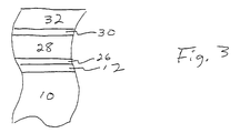
- FIGURE 3 illustrates such an arrangement.
- a germanium layer 12 is utilized on top of the silicon substrate 10, with a SrHfTiO3 layer 26 on top of the germanium layer 12.
- a Bi4Ti3O12 layer 28 is on the SrHfTiO3 layer 26 and a top buffer layer of BaSrTiO3 30 is on top of the Bi4Ti3O12 28 .
- a titanium tungsten top electrode 32 is then deposited atop the second buffer layer 26.
- a second germanium layer (not shown) could be inserted between the BaSrTiO3 30 and the titanium tungsten top electrode 32.
- germanium layer allows the usage of a wider variety of conductors for the top electrode and allows higher temperature processing during and after the deposition of the top electrode, as the germanium generally prevents reaction between the top electrode material and the ferroelectric material.
- the prior art materials generally either form a silicide (e.g. of palladium, platinum or titanium) which allows the diffusion of silicon into the high dielectric materials , or react with silicon (e.g. tin dioxide) or react with the high dielectric oxide to form low dielectric constant insulators (e.g. titanium monoxide or tantalum pentoxide).
- a silicide e.g. of palladium, platinum or titanium
- silicon e.g. tin dioxide
- low dielectric constant insulators e.g. titanium monoxide or tantalum pentoxide
- germanium doped or undoped gives a conductor or semiconductor which reacts neither with the semiconductor substrate nor the high dielectric constant oxide at the required annealling temperatures, and only germanium provides for epitaxial growth of a conductive or semiconductive material on a semiconductor substrate, in a matter compatible with growing and annealing of a high dielectric constant oxide in a non-reactive manner, such that a metal oxide metal or metal oxide semiconductor structure can be fabricated without the effective dielectric constant being significantly lowered by a low dielectric constant material between the high dielectric constant material and the underlying conductor or semiconductor. Even using germanium, however, does not completely eliminate problems with the Pb/Bi diffusion, and thus a non-Pb/Bi high-dielectric oxide containing buffer layer is still needed.
- high-dielectric constant oxides is to mean oxides with dielectric constants of greater than 100, and preferably greater than 1,000 (barium strontium titanate can have dielectric constants greater than 10,000).
- Many such non-Pb/Bi oxides can be considered to be based on BaTiO3 and includes oxides of the general formula (Ba,Sr,Ca)(Ti,Zr,Hf)O3.
- Many other oxides of the general formula (K,Na,Li)(Ta,Nb)O3 will also work.
- Pb/Bi oxides for the purpose of this invention, generally include perovskites whose component oxides are thermodynamically unstable next to germanium metal and non-Pb/Bi high-dielectric oxides for these purposes generally include perovskites whose component oxides are thermodynamically stable next to germanium metal (even if a germanium layer is not used).
- Pb/Bi oxides include materials such as (Pb,La)ZrTiO3 or (Pb,Mg)NbO3 or Bi4Ti3O12. All these oxides can also be doped with acceptors such as Al, Mg, Mn, or Na, or doners such as La, Nb, or P.
- Other semiconductors can also be used in addition to silicon and gallium arsenide.
Landscapes
- Semiconductor Memories (AREA)
- Physical Vapour Deposition (AREA)
- Formation Of Insulating Films (AREA)
- Semiconductor Integrated Circuits (AREA)
Applications Claiming Priority (2)
| Application Number | Priority Date | Filing Date | Title |
|---|---|---|---|
| US87693092A | 1992-05-01 | 1992-05-01 | |
| US876930 | 2004-06-25 |
Publications (3)
| Publication Number | Publication Date |
|---|---|
| EP0568064A2 true EP0568064A2 (fr) | 1993-11-03 |
| EP0568064A3 EP0568064A3 (fr) | 1994-04-06 |
| EP0568064B1 EP0568064B1 (fr) | 1999-07-14 |
Family
ID=25368867
Family Applications (1)
| Application Number | Title | Priority Date | Filing Date |
|---|---|---|---|
| EP93106971A Expired - Lifetime EP0568064B1 (fr) | 1992-05-01 | 1993-04-29 | Oxydes à haute constante diélectrique contenant du Pb/Bi utilisant une perovskite ne contenant pas de Pb/Bi comme couche barrière |
Country Status (6)
| Country | Link |
|---|---|
| US (3) | US5393352A (fr) |
| EP (1) | EP0568064B1 (fr) |
| JP (1) | JP3285408B2 (fr) |
| KR (1) | KR940006213A (fr) |
| DE (1) | DE69325614T2 (fr) |
| TW (1) | TW232748B (fr) |
Cited By (5)
| Publication number | Priority date | Publication date | Assignee | Title |
|---|---|---|---|---|
| EP0851473A3 (fr) * | 1996-12-23 | 1998-07-22 | Lucent Technologies Inc. | Méthode de fabrication d'une couche à constante diélectrique élevée et son application à une couche d'isolation d'une porte et d'un condensateur |
| EP0926739A1 (fr) * | 1997-12-24 | 1999-06-30 | Texas Instruments Incorporated | Structure et procédé pour un transistor à effet de champ du type MIS |
| US6548854B1 (en) | 1997-12-22 | 2003-04-15 | Agere Systems Inc. | Compound, high-K, gate and capacitor insulator layer |
| EP1223622A3 (fr) * | 2001-01-11 | 2004-07-28 | Fujitsu Limited | Dispositif semi-conducteur et sa méthode de fabrication |
| WO2010116184A1 (fr) | 2009-04-08 | 2010-10-14 | Ulive Enterprises Limited | Oxydes métalliques mélangés |
Families Citing this family (88)
| Publication number | Priority date | Publication date | Assignee | Title |
|---|---|---|---|---|
| EP0568064B1 (fr) * | 1992-05-01 | 1999-07-14 | Texas Instruments Incorporated | Oxydes à haute constante diélectrique contenant du Pb/Bi utilisant une perovskite ne contenant pas de Pb/Bi comme couche barrière |
| US6537830B1 (en) | 1992-10-23 | 2003-03-25 | Symetrix Corporation | Method of making ferroelectric FET with polycrystalline crystallographically oriented ferroelectric material |
| DE69404189T2 (de) * | 1993-03-31 | 1998-01-08 | Texas Instruments Inc | Leicht donatoren-dotierte Elektroden für Materialien mit hoher dielektrischer Konstante |
| US5504041A (en) * | 1994-08-01 | 1996-04-02 | Texas Instruments Incorporated | Conductive exotic-nitride barrier layer for high-dielectric-constant materials |
| US5629229A (en) * | 1995-07-12 | 1997-05-13 | Sharp Kabushiki Kaisha | Metalorganic chemical vapor deposition of (Ba1-x Srx)RuO3 /(Ba1-x Srx)TIO3 /(Ba1-x Srx)TiO3 /(Ba1- Srx)RuO3 capacitors for high dielectric materials |
| JP3274326B2 (ja) * | 1995-09-08 | 2002-04-15 | 株式会社東芝 | 半導体装置およびその製造方法 |
| US5612560A (en) * | 1995-10-31 | 1997-03-18 | Northern Telecom Limited | Electrode structure for ferroelectric capacitors for integrated circuits |
| KR100215861B1 (ko) * | 1996-03-13 | 1999-08-16 | 구본준 | 유전체 박막 제조방법 및 이를 이용한 반도체 장치제조방법 |
| US6455916B1 (en) | 1996-04-08 | 2002-09-24 | Micron Technology, Inc. | Integrated circuit devices containing isolated dielectric material |
| US6023082A (en) * | 1996-08-05 | 2000-02-08 | Lockheed Martin Energy Research Corporation | Strain-based control of crystal anisotropy for perovskite oxides on semiconductor-based material |
| US6074885A (en) * | 1997-11-25 | 2000-06-13 | Radiant Technologies, Inc | Lead titanate isolation layers for use in fabricating PZT-based capacitors and similar structures |
| US6184074B1 (en) | 1997-12-17 | 2001-02-06 | Texas Instruments Incorporated | Method of fabrication a self-aligned polysilicon/diffusion barrier/oxygen stable sidewall bottom electrode structure for high-K DRAMS |
| US6180446B1 (en) | 1997-12-17 | 2001-01-30 | Texas Instruments Incorporated | Method of fabricating an oxygen-stable layer/diffusion barrier/poly bottom electrode structure for high-K DRAMS using disposable-oxide processing |
| US6171898B1 (en) | 1997-12-17 | 2001-01-09 | Texas Instruments Incorporated | Method of fabricating an oxygen-stable layer/diffusion barrier/poly bottom electrode structure for high-K-DRAMS using a disposable-oxide processing |
| US5998225A (en) * | 1997-12-17 | 1999-12-07 | Texas Instruments Incorporated | Method of fabricating an oxygen-stable layer/diffusion barrier/poly bottom electrode structure for high-K DRAMs using disposable-oxide processing |
| KR100275121B1 (ko) | 1997-12-30 | 2001-01-15 | 김영환 | 강유전체 캐패시터 제조방법 |
| KR100436059B1 (ko) * | 1997-12-30 | 2004-12-17 | 주식회사 하이닉스반도체 | 강유전체 캐패시터 형성 방법 |
| KR100275726B1 (ko) * | 1997-12-31 | 2000-12-15 | 윤종용 | 강유전체 메모리 장치 및 그 제조 방법 |
| KR100321714B1 (ko) * | 1998-12-30 | 2002-05-09 | 박종섭 | 반도체메모리소자의캐패시터제조방법 |
| US6340827B1 (en) * | 1999-01-13 | 2002-01-22 | Agere Systems Guardian Corp. | Diffusion barrier for use with high dielectric constant materials and electronic devices incorporating same |
| US6248459B1 (en) | 1999-03-22 | 2001-06-19 | Motorola, Inc. | Semiconductor structure having a crystalline alkaline earth metal oxide interface with silicon |
| US6241821B1 (en) | 1999-03-22 | 2001-06-05 | Motorola, Inc. | Method for fabricating a semiconductor structure having a crystalline alkaline earth metal oxide interface with silicon |
| US6270568B1 (en) * | 1999-07-15 | 2001-08-07 | Motorola, Inc. | Method for fabricating a semiconductor structure with reduced leakage current density |
| US6215644B1 (en) | 1999-09-09 | 2001-04-10 | Jds Uniphase Inc. | High frequency tunable capacitors |
| KR100340951B1 (ko) * | 1999-11-18 | 2002-06-22 | 윤덕용 | 초고집적도 디램 커패시터용 스트론튬-납 티탄산 박막의 제조방법 |
| US6496351B2 (en) | 1999-12-15 | 2002-12-17 | Jds Uniphase Inc. | MEMS device members having portions that contact a substrate and associated methods of operating |
| US6229684B1 (en) | 1999-12-15 | 2001-05-08 | Jds Uniphase Inc. | Variable capacitor and associated fabrication method |
| US6291319B1 (en) * | 1999-12-17 | 2001-09-18 | Motorola, Inc. | Method for fabricating a semiconductor structure having a stable crystalline interface with silicon |
| US6479173B1 (en) | 1999-12-17 | 2002-11-12 | Motorola, Inc. | Semiconductor structure having a crystalline alkaline earth metal silicon nitride/oxide interface with silicon |
| US6693033B2 (en) | 2000-02-10 | 2004-02-17 | Motorola, Inc. | Method of removing an amorphous oxide from a monocrystalline surface |
| US6392257B1 (en) | 2000-02-10 | 2002-05-21 | Motorola Inc. | Semiconductor structure, semiconductor device, communicating device, integrated circuit, and process for fabricating the same |
| JP2001313429A (ja) * | 2000-04-27 | 2001-11-09 | Tdk Corp | 積層薄膜その製造方法および電子デバイス |
| KR20030011083A (ko) * | 2000-05-31 | 2003-02-06 | 모토로라 인코포레이티드 | 반도체 디바이스 및 이를 제조하기 위한 방법 |
| US6410941B1 (en) | 2000-06-30 | 2002-06-25 | Motorola, Inc. | Reconfigurable systems using hybrid integrated circuits with optical ports |
| US6477285B1 (en) | 2000-06-30 | 2002-11-05 | Motorola, Inc. | Integrated circuits with optical signal propagation |
| US6501973B1 (en) | 2000-06-30 | 2002-12-31 | Motorola, Inc. | Apparatus and method for measuring selected physical condition of an animate subject |
| US6427066B1 (en) | 2000-06-30 | 2002-07-30 | Motorola, Inc. | Apparatus and method for effecting communications among a plurality of remote stations |
| US6590236B1 (en) | 2000-07-24 | 2003-07-08 | Motorola, Inc. | Semiconductor structure for use with high-frequency signals |
| AU2001276989A1 (en) * | 2000-07-24 | 2002-02-05 | Motorola, Inc. | Thin-film metallic oxide structure and process for fabricating same |
| AU2001277001A1 (en) * | 2000-07-24 | 2002-02-05 | Motorola, Inc. | Heterojunction tunneling diodes and process for fabricating same |
| US6555946B1 (en) | 2000-07-24 | 2003-04-29 | Motorola, Inc. | Acoustic wave device and process for forming the same |
| US6224669B1 (en) | 2000-09-14 | 2001-05-01 | Motorola, Inc. | Method for fabricating a semiconductor structure having a crystalline alkaline earth metal oxide interface with silicon |
| US6638838B1 (en) | 2000-10-02 | 2003-10-28 | Motorola, Inc. | Semiconductor structure including a partially annealed layer and method of forming the same |
| US6583034B2 (en) | 2000-11-22 | 2003-06-24 | Motorola, Inc. | Semiconductor structure including a compliant substrate having a graded monocrystalline layer and methods for fabricating the structure and semiconductor devices including the structure |
| US6559471B2 (en) | 2000-12-08 | 2003-05-06 | Motorola, Inc. | Quantum well infrared photodetector and method for fabricating same |
| US6563118B2 (en) | 2000-12-08 | 2003-05-13 | Motorola, Inc. | Pyroelectric device on a monocrystalline semiconductor substrate and process for fabricating same |
| US20020096683A1 (en) * | 2001-01-19 | 2002-07-25 | Motorola, Inc. | Structure and method for fabricating GaN devices utilizing the formation of a compliant substrate |
| US6673646B2 (en) | 2001-02-28 | 2004-01-06 | Motorola, Inc. | Growth of compound semiconductor structures on patterned oxide films and process for fabricating same |
| US7046719B2 (en) | 2001-03-08 | 2006-05-16 | Motorola, Inc. | Soft handoff between cellular systems employing different encoding rates |
| WO2002082551A1 (fr) | 2001-04-02 | 2002-10-17 | Motorola, Inc. | Structure de semi-conducteur a courant de fuite attenue |
| US6593833B2 (en) | 2001-04-04 | 2003-07-15 | Mcnc | Tunable microwave components utilizing ferroelectric and ferromagnetic composite dielectrics and methods for making same |
| US6709989B2 (en) | 2001-06-21 | 2004-03-23 | Motorola, Inc. | Method for fabricating a semiconductor structure including a metal oxide interface with silicon |
| US6992321B2 (en) | 2001-07-13 | 2006-01-31 | Motorola, Inc. | Structure and method for fabricating semiconductor structures and devices utilizing piezoelectric materials |
| US20030010992A1 (en) * | 2001-07-16 | 2003-01-16 | Motorola, Inc. | Semiconductor structure and method for implementing cross-point switch functionality |
| US6531740B2 (en) | 2001-07-17 | 2003-03-11 | Motorola, Inc. | Integrated impedance matching and stability network |
| US6646293B2 (en) | 2001-07-18 | 2003-11-11 | Motorola, Inc. | Structure for fabricating high electron mobility transistors utilizing the formation of complaint substrates |
| US7019332B2 (en) | 2001-07-20 | 2006-03-28 | Freescale Semiconductor, Inc. | Fabrication of a wavelength locker within a semiconductor structure |
| US6498358B1 (en) | 2001-07-20 | 2002-12-24 | Motorola, Inc. | Structure and method for fabricating an electro-optic system having an electrochromic diffraction grating |
| US6693298B2 (en) | 2001-07-20 | 2004-02-17 | Motorola, Inc. | Structure and method for fabricating epitaxial semiconductor on insulator (SOI) structures and devices utilizing the formation of a compliant substrate for materials used to form same |
| US6472694B1 (en) | 2001-07-23 | 2002-10-29 | Motorola, Inc. | Microprocessor structure having a compound semiconductor layer |
| US6855992B2 (en) * | 2001-07-24 | 2005-02-15 | Motorola Inc. | Structure and method for fabricating configurable transistor devices utilizing the formation of a compliant substrate for materials used to form the same |
| US6594414B2 (en) | 2001-07-25 | 2003-07-15 | Motorola, Inc. | Structure and method of fabrication for an optical switch |
| US6667196B2 (en) | 2001-07-25 | 2003-12-23 | Motorola, Inc. | Method for real-time monitoring and controlling perovskite oxide film growth and semiconductor structure formed using the method |
| US6585424B2 (en) | 2001-07-25 | 2003-07-01 | Motorola, Inc. | Structure and method for fabricating an electro-rheological lens |
| US6462360B1 (en) | 2001-08-06 | 2002-10-08 | Motorola, Inc. | Integrated gallium arsenide communications systems |
| US6589856B2 (en) | 2001-08-06 | 2003-07-08 | Motorola, Inc. | Method and apparatus for controlling anti-phase domains in semiconductor structures and devices |
| US6639249B2 (en) | 2001-08-06 | 2003-10-28 | Motorola, Inc. | Structure and method for fabrication for a solid-state lighting device |
| US20030034491A1 (en) | 2001-08-14 | 2003-02-20 | Motorola, Inc. | Structure and method for fabricating semiconductor structures and devices for detecting an object |
| US6673667B2 (en) | 2001-08-15 | 2004-01-06 | Motorola, Inc. | Method for manufacturing a substantially integral monolithic apparatus including a plurality of semiconductor materials |
| US20030036217A1 (en) * | 2001-08-16 | 2003-02-20 | Motorola, Inc. | Microcavity semiconductor laser coupled to a waveguide |
| US20030071327A1 (en) * | 2001-10-17 | 2003-04-17 | Motorola, Inc. | Method and apparatus utilizing monocrystalline insulator |
| US6916717B2 (en) | 2002-05-03 | 2005-07-12 | Motorola, Inc. | Method for growing a monocrystalline oxide layer and for fabricating a semiconductor device on a monocrystalline substrate |
| US7452757B2 (en) * | 2002-05-07 | 2008-11-18 | Asm America, Inc. | Silicon-on-insulator structures and methods |
| US20040012037A1 (en) * | 2002-07-18 | 2004-01-22 | Motorola, Inc. | Hetero-integration of semiconductor materials on silicon |
| US20040070312A1 (en) * | 2002-10-10 | 2004-04-15 | Motorola, Inc. | Integrated circuit and process for fabricating the same |
| US20040069991A1 (en) * | 2002-10-10 | 2004-04-15 | Motorola, Inc. | Perovskite cuprate electronic device structure and process |
| US7169619B2 (en) | 2002-11-19 | 2007-01-30 | Freescale Semiconductor, Inc. | Method for fabricating semiconductor structures on vicinal substrates using a low temperature, low pressure, alkaline earth metal-rich process |
| US6885065B2 (en) | 2002-11-20 | 2005-04-26 | Freescale Semiconductor, Inc. | Ferromagnetic semiconductor structure and method for forming the same |
| AU2003302958A1 (en) * | 2002-12-17 | 2004-07-09 | Eun, Jaehwan | Method for preparation of ferroelectric single crystal film structure using deposition method |
| US6965128B2 (en) * | 2003-02-03 | 2005-11-15 | Freescale Semiconductor, Inc. | Structure and method for fabricating semiconductor microresonator devices |
| US7020374B2 (en) * | 2003-02-03 | 2006-03-28 | Freescale Semiconductor, Inc. | Optical waveguide structure and method for fabricating the same |
| US20040164315A1 (en) * | 2003-02-25 | 2004-08-26 | Motorola, Inc. | Structure and device including a tunneling piezoelectric switch and method of forming same |
| US8592294B2 (en) * | 2010-02-22 | 2013-11-26 | Asm International N.V. | High temperature atomic layer deposition of dielectric oxides |
| EP3670708A1 (fr) | 2018-12-20 | 2020-06-24 | IMEC vzw | Oxydes de pérovskite selon l'axe a |
| US11903218B2 (en) * | 2020-06-26 | 2024-02-13 | Sandisk Technologies Llc | Bonded memory devices and methods of making the same |
| US12563973B2 (en) | 2020-06-26 | 2026-02-24 | SanDisk Technologies, Inc. | Bonded memory devices and methods of making the same |
| US12362301B2 (en) | 2020-06-26 | 2025-07-15 | SanDisk Technologies, Inc. | Bonded memory devices and methods of making the same |
| US12581665B2 (en) | 2023-08-22 | 2026-03-17 | SanDisk Technologies, Inc. | Bonded memory MRAM arrays sharing a common driver circuit and methods of making the same |
Family Cites Families (11)
| Publication number | Priority date | Publication date | Assignee | Title |
|---|---|---|---|---|
| US4994435A (en) * | 1987-10-16 | 1991-02-19 | The Furukawa Electric Co., Ltd. | Laminated layers of a substrate, noble metal, and interlayer underneath an oxide superconductor |
| US5179070A (en) * | 1988-04-30 | 1993-01-12 | Sumitomo Electric Industries, Ltd. | Semiconductor substrate having a superconducting thin film with a buffer layer in between |
| KR920704360A (ko) * | 1990-02-26 | 1992-12-19 | 시메트릭스 코포레이션 | 전자장치, 메모리 매트릭스 및 그 신경망 |
| JPH0488685A (ja) * | 1990-07-31 | 1992-03-23 | Matsushita Electric Ind Co Ltd | 薄膜基板およびその製造方法 |
| US5173835A (en) * | 1991-10-15 | 1992-12-22 | Motorola, Inc. | Voltage variable capacitor |
| DE59203461D1 (de) * | 1991-11-04 | 1995-10-05 | Asea Brown Boveri | Speiseschaltung für eine Zweirohr-Hydraulik. |
| EP0540993A1 (fr) * | 1991-11-06 | 1993-05-12 | Ramtron International Corporation | Structure et fabrication d'un transistor à effet de champ de type MOS à haute transconductance en utilisant un empilement de couches couche tampon/ferroélectrique/couche tampon comme diélectrique de porte |
| US5338951A (en) * | 1991-11-06 | 1994-08-16 | Ramtron International Corporation | Structure of high dielectric constant metal/dielectric/semiconductor capacitor for use as the storage capacitor in memory devices |
| EP0568064B1 (fr) * | 1992-05-01 | 1999-07-14 | Texas Instruments Incorporated | Oxydes à haute constante diélectrique contenant du Pb/Bi utilisant une perovskite ne contenant pas de Pb/Bi comme couche barrière |
| US5326721A (en) * | 1992-05-01 | 1994-07-05 | Texas Instruments Incorporated | Method of fabricating high-dielectric constant oxides on semiconductors using a GE buffer layer |
| US5471364A (en) * | 1993-03-31 | 1995-11-28 | Texas Instruments Incorporated | Electrode interface for high-dielectric-constant materials |
-
1993
- 1993-04-29 EP EP93106971A patent/EP0568064B1/fr not_active Expired - Lifetime
- 1993-04-29 DE DE69325614T patent/DE69325614T2/de not_active Expired - Fee Related
- 1993-04-30 KR KR1019930007401A patent/KR940006213A/ko not_active Ceased
- 1993-04-30 JP JP10455293A patent/JP3285408B2/ja not_active Expired - Fee Related
- 1993-08-26 TW TW082106903A patent/TW232748B/zh not_active IP Right Cessation
- 1993-09-27 US US08/127,222 patent/US5393352A/en not_active Expired - Lifetime
-
1995
- 1995-02-27 US US08/395,016 patent/US5650646A/en not_active Expired - Lifetime
-
1997
- 1997-04-17 US US08/842,863 patent/US5912486A/en not_active Expired - Lifetime
Cited By (6)
| Publication number | Priority date | Publication date | Assignee | Title |
|---|---|---|---|---|
| EP0851473A3 (fr) * | 1996-12-23 | 1998-07-22 | Lucent Technologies Inc. | Méthode de fabrication d'une couche à constante diélectrique élevée et son application à une couche d'isolation d'une porte et d'un condensateur |
| US6548854B1 (en) | 1997-12-22 | 2003-04-15 | Agere Systems Inc. | Compound, high-K, gate and capacitor insulator layer |
| EP0926739A1 (fr) * | 1997-12-24 | 1999-06-30 | Texas Instruments Incorporated | Structure et procédé pour un transistor à effet de champ du type MIS |
| US6287903B1 (en) | 1997-12-24 | 2001-09-11 | Texas Instruments Incorporated | Structure and method for a large-permittivity dielectric using a germanium layer |
| EP1223622A3 (fr) * | 2001-01-11 | 2004-07-28 | Fujitsu Limited | Dispositif semi-conducteur et sa méthode de fabrication |
| WO2010116184A1 (fr) | 2009-04-08 | 2010-10-14 | Ulive Enterprises Limited | Oxydes métalliques mélangés |
Also Published As
| Publication number | Publication date |
|---|---|
| US5393352A (en) | 1995-02-28 |
| DE69325614T2 (de) | 2000-01-13 |
| TW232748B (fr) | 1994-10-21 |
| DE69325614D1 (de) | 1999-08-19 |
| EP0568064B1 (fr) | 1999-07-14 |
| KR940006213A (ko) | 1994-03-23 |
| JPH06224184A (ja) | 1994-08-12 |
| JP3285408B2 (ja) | 2002-05-27 |
| US5650646A (en) | 1997-07-22 |
| EP0568064A3 (fr) | 1994-04-06 |
| US5912486A (en) | 1999-06-15 |
Similar Documents
| Publication | Publication Date | Title |
|---|---|---|
| US5650646A (en) | Pb/Bi-containing high-dielectric constant oxides using a non-Pb/Bi-containing perovskite as a buffer layer | |
| US5326721A (en) | Method of fabricating high-dielectric constant oxides on semiconductors using a GE buffer layer | |
| US6287903B1 (en) | Structure and method for a large-permittivity dielectric using a germanium layer | |
| US5635741A (en) | Barium strontium titanate (BST) thin films by erbium donor doping | |
| US5801105A (en) | Multilayer thin film, substrate for electronic device, electronic device, and preparation of multilayer oxide thin film | |
| EP0766292B1 (fr) | Méthode de fabrication d'un élément à couche ferroélectrique et élément à couche ferroélectrique et élément ferroélectrique fabriqué par cette méthode | |
| US8088659B2 (en) | Method of forming capacitors | |
| US5626906A (en) | Electrodes comprising conductive perovskite-seed layers for perovskite dielectrics | |
| US5453908A (en) | Barium strontium titanate (BST) thin films by holmium donor doping | |
| US6285048B1 (en) | Barium strontium titanate integrated circuit capacitors and process for making the same | |
| JP2002530862A (ja) | 水素ダメージを受けた強誘電体膜の不活性ガス回復アニーリング | |
| US6864146B2 (en) | Metal oxide integrated circuit on silicon germanium substrate | |
| KR100378276B1 (ko) | 절연 재료, 절연막 피복 기판, 그 제조 방법 및 박막 소자 | |
| JP3994468B2 (ja) | 酸化物積層構造およびその製造方法ならびに強誘電体不揮発性メモリ | |
| JP2002076292A (ja) | 金属酸化物誘電体膜 | |
| JP2002334875A (ja) | 金属酸化物誘電体膜の気相成長方法 | |
| JPH05343617A (ja) | 半導体記憶装置 | |
| JP2000216360A (ja) | 半導体メモリ素子 |
Legal Events
| Date | Code | Title | Description |
|---|---|---|---|
| PUAI | Public reference made under article 153(3) epc to a published international application that has entered the european phase |
Free format text: ORIGINAL CODE: 0009012 |
|
| AK | Designated contracting states |
Kind code of ref document: A2 Designated state(s): DE FR GB IT |
|
| PUAL | Search report despatched |
Free format text: ORIGINAL CODE: 0009013 |
|
| AK | Designated contracting states |
Kind code of ref document: A3 Designated state(s): DE FR GB IT |
|
| 17P | Request for examination filed |
Effective date: 19940912 |
|
| 17Q | First examination report despatched |
Effective date: 19960320 |
|
| GRAG | Despatch of communication of intention to grant |
Free format text: ORIGINAL CODE: EPIDOS AGRA |
|
| GRAG | Despatch of communication of intention to grant |
Free format text: ORIGINAL CODE: EPIDOS AGRA |
|
| GRAH | Despatch of communication of intention to grant a patent |
Free format text: ORIGINAL CODE: EPIDOS IGRA |
|
| GRAH | Despatch of communication of intention to grant a patent |
Free format text: ORIGINAL CODE: EPIDOS IGRA |
|
| ITF | It: translation for a ep patent filed | ||
| GRAA | (expected) grant |
Free format text: ORIGINAL CODE: 0009210 |
|
| AK | Designated contracting states |
Kind code of ref document: B1 Designated state(s): DE FR GB IT |
|
| REF | Corresponds to: |
Ref document number: 69325614 Country of ref document: DE Date of ref document: 19990819 |
|
| ET | Fr: translation filed | ||
| PLBE | No opposition filed within time limit |
Free format text: ORIGINAL CODE: 0009261 |
|
| 26N | No opposition filed | ||
| REG | Reference to a national code |
Ref country code: GB Ref legal event code: IF02 |
|
| PGFP | Annual fee paid to national office [announced via postgrant information from national office to epo] |
Ref country code: IT Payment date: 20070628 Year of fee payment: 15 |
|
| PGFP | Annual fee paid to national office [announced via postgrant information from national office to epo] |
Ref country code: GB Payment date: 20080317 Year of fee payment: 16 |
|
| PGFP | Annual fee paid to national office [announced via postgrant information from national office to epo] |
Ref country code: DE Payment date: 20080430 Year of fee payment: 16 |
|
| PGFP | Annual fee paid to national office [announced via postgrant information from national office to epo] |
Ref country code: FR Payment date: 20080403 Year of fee payment: 16 |
|
| PG25 | Lapsed in a contracting state [announced via postgrant information from national office to epo] |
Ref country code: IT Free format text: LAPSE BECAUSE OF NON-PAYMENT OF DUE FEES Effective date: 20080429 |
|
| GBPC | Gb: european patent ceased through non-payment of renewal fee |
Effective date: 20090429 |
|
| REG | Reference to a national code |
Ref country code: FR Ref legal event code: ST Effective date: 20091231 |
|
| PG25 | Lapsed in a contracting state [announced via postgrant information from national office to epo] |
Ref country code: DE Free format text: LAPSE BECAUSE OF NON-PAYMENT OF DUE FEES Effective date: 20091103 |
|
| PG25 | Lapsed in a contracting state [announced via postgrant information from national office to epo] |
Ref country code: GB Free format text: LAPSE BECAUSE OF NON-PAYMENT OF DUE FEES Effective date: 20090429 Ref country code: FR Free format text: LAPSE BECAUSE OF NON-PAYMENT OF DUE FEES Effective date: 20091222 |