EP0568330A2 - Verfahren und Gerät zur programmierbaren integrierten Schaltungsdiagnose - Google Patents
Verfahren und Gerät zur programmierbaren integrierten Schaltungsdiagnose Download PDFInfo
- Publication number
- EP0568330A2 EP0568330A2 EP93303303A EP93303303A EP0568330A2 EP 0568330 A2 EP0568330 A2 EP 0568330A2 EP 93303303 A EP93303303 A EP 93303303A EP 93303303 A EP93303303 A EP 93303303A EP 0568330 A2 EP0568330 A2 EP 0568330A2
- Authority
- EP
- European Patent Office
- Prior art keywords
- combinatorial logic
- logic circuit
- output
- gate
- signals
- Prior art date
- Legal status (The legal status is an assumption and is not a legal conclusion. Google has not performed a legal analysis and makes no representation as to the accuracy of the status listed.)
- Withdrawn
Links
Images




Classifications
-
- G—PHYSICS
- G06—COMPUTING OR CALCULATING; COUNTING
- G06F—ELECTRIC DIGITAL DATA PROCESSING
- G06F11/00—Error detection; Error correction; Monitoring
- G06F11/22—Detection or location of defective computer hardware by testing during standby operation or during idle time, e.g. start-up testing
-
- G—PHYSICS
- G01—MEASURING; TESTING
- G01R—MEASURING ELECTRIC VARIABLES; MEASURING MAGNETIC VARIABLES
- G01R31/00—Arrangements for testing electric properties; Arrangements for locating electric faults; Arrangements for electrical testing characterised by what is being tested not provided for elsewhere
- G01R31/28—Testing of electronic circuits, e.g. by signal tracer
- G01R31/317—Testing of digital circuits
- G01R31/3181—Functional testing
- G01R31/3185—Reconfiguring for testing, e.g. LSSD, partitioning
Definitions
- This invention pertains to integrated circuit architecture such as network controller architecture which permits the user to program the functions of network system diagnostic circuitry.
- Figure 1 is a block diagram disclosing one technique for programming the AND and OR Diagnostic Registers.
- Figure 2 is a block diagram of the circuit of one embodiment of a diagnostic channel.
- microprocessors As a part of a chip. Other chips are designed with internal bus architecture and interfacing to standard buses of computer systems. Access to microprocesses bus structure provides the opportunity to program such chips with firmware or software under user control in ways not heretofore possible. For example, programming system status or self check diagnostics is now possible and theoretically if the chip were physically designed so as to make all its nodes available to detectors, a user could program a self check for every node, compare the result to a standard, and provide an error indicator of out of spec conditions and/or initiate a corrective action.
- Control Register 8 is another set of registers for pins o through n, illustrated as Control Register 8 and Control Register N, 8'.
- the Control Registers (8...8') are also programmable via port 11 and peripheral 17 in the same manner as explained regarding AND Registers and OR Registers.
- the hardware interconnections to enable control of the diagnostic signal output for each of the dedicated pins is shown.
- the circuitry of Figure 2 is identical for each of the "i" dedicated diagnostic pins.
- the chip designer has provided metallization interconnection lines 38 on the chip connecting M nodes 37 to be available for diagnosis to a block of programmable AND gates 35' and via M interconnection lines 39 to a block of programmable OR gates 40'.
- the chip designer has also provided metallization 36 on the chip connecting the outputs of each stage of the programmable AND Register 6 to the Programmable AND gates 35' and programmable OR Register 7 stage outputs to the Programmable OR gates 40'.
- the number of stages of the AND register 6 and OR register 7 must equal the number "m" of the diagnostic nodes made available for the "i" pin.
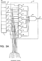
- the programmed AND Register 6 is shown connected via lines 50-57 to the Programmable AND gates block 35', each stage of the AND Register 6 being connected to a respective AND gate 58-65.
- a second input to each AND gate 58-65 are the Diagnostic Nodes O through M, with one node, I through M, coupled to a specific AND gate. If the user were to have programmed AND register 6 so that one of the register stages is a high, for example the first stage, and the remainder were programmed at a low value, then only AND gate 58 would respond, so that Diagnostic Node O would be the only state being designated to be monitored.
- Control Register 8 By setting the "Control Registers" for each of the dedicated bits, additional programmability is obtained.
- the first bit of Control Register 8 is set to enable selection of either the AND gate block 35' or the OR gate block 40'. This is shown on Figure 2 as a Register ANDOR bit 32 connected to the MUX46 causing the MUX to switch its output between the lines 44 and 45.
- the second bit of the Control Register is designated "polarity bit” 33 and it causes switching of polarity of the output by inverting the XOR circuit 48.
- the third bit of the Control Register is designated "Stretch bit" 34 which is connected to a pair of AND gates 49 and 50.
- Stretch bit 34 When Stretch bit is low, AND gate 50 causes the signal from the XOR 48 to bypass the pulse stretcher 51 on line 52. If the Stretch bit 34 is high, the output of the XOR 48 is coupled through stretcher circuit 51 then to the output 53 to Pinout i.
- the stretcher function permits certain short duration pulses to be lengthened so that they may be visibly perceived by a human observer. In addition, the stretcher function can be configured for LED blinking excitation.
- FIG. 4 Another embodiment is disclosed which feeds the pulse stretcher 93 back via connection 92 to the MUX 94 on the non-selected inverted input.
- the block 90 a differently programmable block, similar to the source block 95, indicates an error, it would take over control via control line and causes the MUX 94 to feed back the pulse stretcher output to its input which would result in an oscillation which would cause an LED i to continually blink as an alarm indication.
- the pulse stretch 51 and 93 could be as simple as a divider circuit such as a ripple counter described in "Logic Design with Integrated Circuits," by William Wickes, John Wiley and Sons, 1968, at page 198.
- the pulse stretcher could have programmable on and off times.
- This invention finds particular application in an Ethernet network controller chip where it is desirable to have network status activities displayed with LEDs.
- Collision There are six primary network indicators called Collision, Jabber, Link Status, Receive, Receive Polarity and Transmit and several other secondary indicators.
Landscapes
- Engineering & Computer Science (AREA)
- General Engineering & Computer Science (AREA)
- Physics & Mathematics (AREA)
- General Physics & Mathematics (AREA)
- Theoretical Computer Science (AREA)
- Computer Hardware Design (AREA)
- Quality & Reliability (AREA)
- Test And Diagnosis Of Digital Computers (AREA)
- Tests Of Electronic Circuits (AREA)
Applications Claiming Priority (2)
| Application Number | Priority Date | Filing Date | Title |
|---|---|---|---|
| US07/877,566 US5479649A (en) | 1992-05-01 | 1992-05-01 | Method and apparatus for forming a logical combination of signals from diagnostic nodes in an IC chip for passive observation at a dedicated diagnostic pin |
| US877566 | 1992-05-01 |
Publications (2)
| Publication Number | Publication Date |
|---|---|
| EP0568330A2 true EP0568330A2 (de) | 1993-11-03 |
| EP0568330A3 EP0568330A3 (de) | 1997-12-03 |
Family
ID=25370240
Family Applications (1)
| Application Number | Title | Priority Date | Filing Date |
|---|---|---|---|
| EP93303303A Withdrawn EP0568330A3 (de) | 1992-05-01 | 1993-04-28 | Verfahren und Gerät zur programmierbaren integrierten Schaltungsdiagnose |
Country Status (4)
| Country | Link |
|---|---|
| US (1) | US5479649A (de) |
| EP (1) | EP0568330A3 (de) |
| JP (1) | JPH0634718A (de) |
| KR (1) | KR930024127A (de) |
Families Citing this family (6)
| Publication number | Priority date | Publication date | Assignee | Title |
|---|---|---|---|---|
| JPH0540730A (ja) * | 1991-08-06 | 1993-02-19 | Mitsubishi Electric Corp | マイクロコンピユータ |
| JP2845155B2 (ja) * | 1995-02-07 | 1999-01-13 | 日本電気株式会社 | シングルチップマイクロコンピュータのエミュレーションチップ |
| KR100247012B1 (ko) * | 1997-05-15 | 2000-03-15 | 윤종용 | 통신시스템의 상태정보 수집 및 제어장치 |
| US6968545B1 (en) * | 2000-09-11 | 2005-11-22 | Agilent Technologies, Inc. | Method and apparatus for no-latency conditional branching |
| JP2003244132A (ja) * | 2002-02-18 | 2003-08-29 | Mitsubishi Electric Corp | スクランブラおよびデスクランブラ |
| KR100751534B1 (ko) * | 2007-04-17 | 2007-08-22 | (주)다산컨설턴트 | 연속 침전여과형 초기우수 처리장치 |
Family Cites Families (20)
| Publication number | Priority date | Publication date | Assignee | Title |
|---|---|---|---|---|
| US3825901A (en) * | 1972-11-09 | 1974-07-23 | Ibm | Integrated diagnostic tool |
| JPS5483341A (en) * | 1977-12-15 | 1979-07-03 | Nec Corp | Digital integrated circuit |
| JPS5853774B2 (ja) * | 1978-12-29 | 1983-12-01 | 株式会社日立製作所 | 情報処理装置 |
| IN155448B (de) * | 1980-03-19 | 1985-02-02 | Int Computers Ltd | |
| US4371952A (en) * | 1981-05-06 | 1983-02-01 | Ncr Corporation | Diagnostic circuitry for isolating a faulty subsystem in a data processing system |
| JPS58146834A (ja) * | 1982-02-24 | 1983-09-01 | Sumitomo Metal Ind Ltd | 炉体耐火物状態の推定方法 |
| JPS6013266A (ja) * | 1983-07-04 | 1985-01-23 | Hitachi Ltd | 診断容易化回路 |
| ATE128291T1 (de) * | 1985-12-06 | 1995-10-15 | Advanced Micro Devices Inc | Programmierbare logische schaltung mit konfigurierbarer freigabe des ausgangs. |
| US4758747A (en) * | 1986-05-30 | 1988-07-19 | Advanced Micro Devices, Inc. | Programmable logic device with buried registers selectively multiplexed with output registers to ports, and preload circuitry therefor |
| US4703484A (en) * | 1985-12-19 | 1987-10-27 | Harris Corporation | Programmable integrated circuit fault detection apparatus |
| US4755967A (en) * | 1986-03-21 | 1988-07-05 | Monolithic Memories, Inc. | Programmable synchronous sequential state machine or sequencer having decision variable input mapping circuit responsive to feedback signals |
| US4752729A (en) * | 1986-07-01 | 1988-06-21 | Texas Instruments Incorporated | Test circuit for VSLI integrated circuits |
| US5012180A (en) * | 1988-05-17 | 1991-04-30 | Zilog, Inc. | System for testing internal nodes |
| US4975641A (en) * | 1988-07-14 | 1990-12-04 | Sharp Kabushiki Kaisha | Integrated circuit and method for testing the integrated circuit |
| US4995038A (en) * | 1988-07-28 | 1991-02-19 | Digital Equipment Corporation | Finding faults in circuit boards |
| CN1045655A (zh) * | 1988-11-23 | 1990-09-26 | 约翰弗兰克制造公司 | 系统自动诊断的内核测试接口和方法 |
| US5157781A (en) * | 1990-01-02 | 1992-10-20 | Motorola, Inc. | Data processor test architecture |
| US5030904A (en) * | 1990-02-13 | 1991-07-09 | Hewlett-Packard Company | Diagnostic system for integrated circuits using existing pads |
| US5253255A (en) * | 1990-11-02 | 1993-10-12 | Intel Corporation | Scan mechanism for monitoring the state of internal signals of a VLSI microprocessor chip |
| US5144230A (en) * | 1990-11-26 | 1992-09-01 | The Boeing Company | Method and system for testing integrated circuits by cycle stealing |
-
1992
- 1992-05-01 US US07/877,566 patent/US5479649A/en not_active Expired - Fee Related
-
1993
- 1993-04-28 EP EP93303303A patent/EP0568330A3/de not_active Withdrawn
- 1993-04-30 JP JP5104142A patent/JPH0634718A/ja active Pending
- 1993-05-01 KR KR1019930007544A patent/KR930024127A/ko not_active Abandoned
Also Published As
| Publication number | Publication date |
|---|---|
| EP0568330A3 (de) | 1997-12-03 |
| JPH0634718A (ja) | 1994-02-10 |
| US5479649A (en) | 1995-12-26 |
| KR930024127A (ko) | 1993-12-22 |
Similar Documents
| Publication | Publication Date | Title |
|---|---|---|
| US6806730B2 (en) | Method and system for use of an embedded field programmable gate array interconnect for flexible I/O connectivity | |
| US4858178A (en) | Programmable sequence generator | |
| EP0253530B1 (de) | Dynamisch rekonfigurierbare Feldlogik | |
| US5521870A (en) | Semiconductor memory device having a coincidence detection circuit and its test method | |
| US8482313B2 (en) | Universal digital block interconnection and channel routing | |
| US4460997A (en) | Memory tester having memory repair analysis capability | |
| US5956252A (en) | Method and apparatus for an integrated circuit that is reconfigurable based on testing results | |
| JPH07119789B2 (ja) | 半導体集積回路装置及びその診断方法 | |
| US4862072A (en) | Distributed access serial port test arrangement for integrated circuits | |
| US5497107A (en) | Multiple, selectable PLAS having shared inputs and outputs | |
| US5027012A (en) | Programmable logic circuit using wired-or tristate gates | |
| EP0568330A2 (de) | Verfahren und Gerät zur programmierbaren integrierten Schaltungsdiagnose | |
| US4458163A (en) | Programmable architecture logic | |
| US4322812A (en) | Digital data processor providing for monitoring, changing and loading of RAM instruction data | |
| US5420870A (en) | Non-fully-decoded test address generator | |
| US6546510B1 (en) | Burn-in mode detect circuit for semiconductor device | |
| US6157051A (en) | Multiple function array based application specific integrated circuit | |
| KR900003884A (ko) | 대규모 반도체 집적회로 장치 | |
| US5036495A (en) | Multiple mode-set for IC chip | |
| US7058778B2 (en) | Memory controllers having pins with selectable functionality | |
| DE19651248B4 (de) | Betriebsmodussetzschaltung in einer Halbleitereinrichtung | |
| US7395445B1 (en) | Controller for power supplies | |
| EP1482411B1 (de) | Fehlererkennung in einem Schaltkreis-Modul | |
| US4874968A (en) | Component produced using integrated technology for the fabrication of integrated circuits | |
| US20010039608A1 (en) | Architecture and configuring method for a computer expansion board |
Legal Events
| Date | Code | Title | Description |
|---|---|---|---|
| PUAI | Public reference made under article 153(3) epc to a published international application that has entered the european phase |
Free format text: ORIGINAL CODE: 0009012 |
|
| AK | Designated contracting states |
Kind code of ref document: A2 Designated state(s): BE DE DK ES FR GB GR IE IT LU NL PT |
|
| PUAL | Search report despatched |
Free format text: ORIGINAL CODE: 0009013 |
|
| AK | Designated contracting states |
Kind code of ref document: A3 Designated state(s): BE DE DK ES FR GB GR IE IT LU NL PT |
|
| 17P | Request for examination filed |
Effective date: 19980408 |
|
| 17Q | First examination report despatched |
Effective date: 19990830 |
|
| STAA | Information on the status of an ep patent application or granted ep patent |
Free format text: STATUS: THE APPLICATION HAS BEEN WITHDRAWN |
|
| 18W | Application withdrawn |
Withdrawal date: 20010810 |