EP0570145B1 - Steuerschaltung - Google Patents
Steuerschaltung Download PDFInfo
- Publication number
- EP0570145B1 EP0570145B1 EP93303461A EP93303461A EP0570145B1 EP 0570145 B1 EP0570145 B1 EP 0570145B1 EP 93303461 A EP93303461 A EP 93303461A EP 93303461 A EP93303461 A EP 93303461A EP 0570145 B1 EP0570145 B1 EP 0570145B1
- Authority
- EP
- European Patent Office
- Prior art keywords
- signal
- sim card
- circuit
- voltage
- receiver means
- Prior art date
- Legal status (The legal status is an assumption and is not a legal conclusion. Google has not performed a legal analysis and makes no representation as to the accuracy of the status listed.)
- Expired - Lifetime
Links
- 238000005259 measurement Methods 0.000 claims description 21
- 239000003990 capacitor Substances 0.000 claims description 16
- 230000001419 dependent effect Effects 0.000 claims description 8
- 230000007423 decrease Effects 0.000 claims description 7
- 238000000034 method Methods 0.000 claims description 3
- 230000009849 deactivation Effects 0.000 claims description 2
- 230000003213 activating effect Effects 0.000 description 2
- 230000006870 function Effects 0.000 description 2
- 238000012544 monitoring process Methods 0.000 description 2
- 238000013461 design Methods 0.000 description 1
- 230000008030 elimination Effects 0.000 description 1
- 238000003379 elimination reaction Methods 0.000 description 1
- 238000003780 insertion Methods 0.000 description 1
- 230000037431 insertion Effects 0.000 description 1
- 238000012986 modification Methods 0.000 description 1
- 230000004048 modification Effects 0.000 description 1
Images
Classifications
-
- H—ELECTRICITY
- H04—ELECTRIC COMMUNICATION TECHNIQUE
- H04W—WIRELESS COMMUNICATION NETWORKS
- H04W52/00—Power management, e.g. Transmission Power Control [TPC] or power classes
- H04W52/02—Power saving arrangements
- H04W52/0209—Power saving arrangements in terminal devices
- H04W52/0251—Power saving arrangements in terminal devices using monitoring of local events, e.g. events related to user activity
- H04W52/0254—Power saving arrangements in terminal devices using monitoring of local events, e.g. events related to user activity detecting a user operation or a tactile contact or a motion of the device
-
- H—ELECTRICITY
- H04—ELECTRIC COMMUNICATION TECHNIQUE
- H04W—WIRELESS COMMUNICATION NETWORKS
- H04W52/00—Power management, e.g. Transmission Power Control [TPC] or power classes
- H04W52/02—Power saving arrangements
- H04W52/0209—Power saving arrangements in terminal devices
- H04W52/0261—Power saving arrangements in terminal devices managing power supply demand, e.g. depending on battery level
-
- Y—GENERAL TAGGING OF NEW TECHNOLOGICAL DEVELOPMENTS; GENERAL TAGGING OF CROSS-SECTIONAL TECHNOLOGIES SPANNING OVER SEVERAL SECTIONS OF THE IPC; TECHNICAL SUBJECTS COVERED BY FORMER USPC CROSS-REFERENCE ART COLLECTIONS [XRACs] AND DIGESTS
- Y02—TECHNOLOGIES OR APPLICATIONS FOR MITIGATION OR ADAPTATION AGAINST CLIMATE CHANGE
- Y02D—CLIMATE CHANGE MITIGATION TECHNOLOGIES IN INFORMATION AND COMMUNICATION TECHNOLOGIES [ICT], I.E. INFORMATION AND COMMUNICATION TECHNOLOGIES AIMING AT THE REDUCTION OF THEIR OWN ENERGY USE
- Y02D30/00—Reducing energy consumption in communication networks
- Y02D30/70—Reducing energy consumption in communication networks in wireless communication networks
Definitions
- the present invention relates to a control circuit for selectively deactivating a device.
- the control circuit of the present invention is intended for use with devices which utilize user identity cards such as a subscriber identity module (SIM) suitable for use in mobile telephone systems such as the Group Special Mobile (GSM) system.
- SIM subscriber identity module
- GSM Group Special Mobile
- the mobile telephone In terms of the specification of a GSM mobile telephone network, the mobile telephone is always provided with a space for inserting a user card.
- the user card contains the user data recorded in the memory of a microchip. With the help of the card data, the system identifies the person using the device, and finds the correct address for billing, among others.
- the mobile telephone may be equipped with a small, semi-stationary user card, which is rarely exchanged. However, a "SIM card" of the size of a credit card is likely to become more frequently used in mobile telephones.
- SIM card of the size of a credit card is likely to become more frequently used in mobile telephones.
- the correct position of the user card is typically detected by a member which stops the normal operation of the telephone if the card is removed.
- PIN Personal Identity Number
- a PIN code corresponding to the one of the card inserted in the telephone having been supplied by the user the device will be ready for use, allowing the user to make several calls, even at long intervals, without having to provide the PIN code anew.
- this is only possible on the condition that the internal supply voltage of the mobile telephone is not interrupted. If the supply voltage of the mobile telephone in a GSM system is interrupted, the user has to feed the PIN code once again before being able to use the telephone.
- Momentary supply voltage breaks may occur, for instance when the mobile telephone is connected to a car, the power being supplied from the accumulator voltage of the car.
- the power supply to accessory devices is interrupted when the car is being started.
- the internal voltage of the mobile telephone is also interrupted, and the PIN code has to be fed once again before the telephone will be ready for use.
- the supply voltage may be interrupted, depending on the telephone design, when the voltage level drops below the reset point of the batteries, and the old battery of the telephone has to be replaced by a freshly charged battery. In such cases, the starting of the car or the exchange of the battery only takes about 30 seconds.
- EP 0 310 284 discloses an automobile telephone device, in which a voltage monitoring unit (monitors the voltage of the battery. When the voltage falls near a limit voltage required for starting the automobile engine, the monitoring unit electrically interrupts a power source line connecting the battery and the telephone device via a proper switch circuit to thereby inhibit excessive consumption of the automobile battery by the automatic answering or receiving function during engine stoppage.
- a voltage monitoring unit monitors the voltage of the battery. When the voltage falls near a limit voltage required for starting the automobile engine, the monitoring unit electrically interrupts a power source line connecting the battery and the telephone device via a proper switch circuit to thereby inhibit excessive consumption of the automobile battery by the automatic answering or receiving function during engine stoppage.
- EP 0 439 319 discloses an automobile radio telephone apparatus capable of detecting a drop of power source voltage to prevent a telephone channel from being occupied wastefully and to thereby enhance efficient use of channels with regard to the operation of an automobile radio telephone system.
- the apparatus informs the user of such an occurrence.
- the apparatus warns the user that it will execute a forcible conversation ending procedure and then executes it.
- EP 0 091 281 discloses a circuit arrangement for detecting restoration of a momentary interruption so that the previous operation can be continued.
- US 4 509 201 discloses a wireless telephone apparatus having protection against power loss.
- a control circuit for selectively deactivating a device, the control circuit comprising a Subscriber Identity Module (SIM) card receiver means which produces a first signal (Swa) when the SIM card is present and a second signal (Swb) when the SIM card is not present, coupled to a measurement circuit the magnitude of the output of the measurement circuit being dependent on the signal from the SIM card receiver means, such that if the first signal (Swa) is emitted by the SIM card receiver means the magnitude of the output from the measurement circuit is dependent on the duration of any interruption in the input voltage to the device and if the second signal (Swb) is emitted by the SIM card receiver means the magnitude of the output from the measurement circuit falls below a predetermined level, the measurement circuit being coupled to a deactivation means which deactivates the device if the magnitude of the signal from the measurement circuit falls below said predetermined level either because the SIM card is not present or because the duration of an interruption in the input voltage has exceeded a predetermined limit.
- SIM Subscriber Identity Module
- a method of determining whether a device should be deactivated comprising the steps of providing an output signal dependent on the duration of any interruption in the input voltage to the device and a signal from a Subscriber Identity Module (SIM) card receiver means, the SIM card receiver means emitting a first signal when a SIM card is present and a second signal when the SIM card is not present, such that the output signal decreases gradually if the input voltage is interrupted and the SIM card is present, and decreases rapidly if the SIM card is not present on the interruption of the input voltage to the device allowing the output signal to decrease on the reinstatement of the input voltage to the device, noting the magnitude of the output signal, waiting a predetermined time period and again noting the magnitude of the output signal, determining the difference in the magnitudes of the output signals measured and determining whether or not the device should be deactivated dependent upon said difference in magnitudes of the output signals.
- SIM Subscriber Identity Module
- An advantage of the invention is the elimination of the need for repeated inputting of the PIN codes caused by short voltage breaks.
- the device is provided with members for detecting whether the user card has remained in its position during a short break of the supply voltage. If the user card has been removed from its position during the break, a signal is generated, and the PIN code is required once again.
- the break duration is detected by a simple RC circuit, by measuring the voltage drop of the capacitor during the break, this being proportional to the break duration.
- a switch member has been provided to discharge the capacitor as the user card is removed from its position.
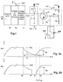
- Figure 1 shows switch member 1 connected to the insertion space of a user card known per se, the switch member being closed, i.e. in position "a" when the SIM user card is inserted, and the switch 1 then generates an output signal Swa.
- switch position "b" shown in the figure, the card has been removed and the switch generates output signal Swb.
- the control circuit comprises an inverter circuit 2 for the switch signal, which inverts output signal Swa or Swb.
- the inverter circuit has been accomplished with a simple transistor switch 3.
- the collector 4 of transistor 3 is connected to the centre of measurement circuit 5 between resistor R1 and capacitor C1.
- the RC circuit is used to measure the duration of the supply voltage break in the manner described below.
- the voltage of capacitor C1 is detected with the member combination DET, which in the example given comprises a voltage detecting circuit 11, e.g. a comparator, which directly generates an activating signal, i.e. output signal Act.
- circuit may comprise a voltage measuring circuit, e.g. a digital/analog converter.
- the output of circuit 11 may be taken to circuit 12, by means of which the voltage data are converted into time data, expressing the duration of the break.
- the output of the converting circuit is connected to terminal circuit 13, which generates output signal Act, if the detected duration of the break has exceeded a predetermined limit value tlim.
- FIG. 2a illustrates the operation of the circuit of figure 1.
- the figure shows voltage Vcl of capacitor C1 as a function of time. Starting from the left in figure 2a, one can see how the voltage of capacitor C1 increases to the approximate value +Vcc, the user card being inserted in the mobile telephone, and the supply voltage having been switched on.
- Output signal Swa of switch 1 is essentially zero and transistor T1 is not conductive, since voltage Vcc passes via diode D1 and resistor R2 directly into the ground.
- the capacitor voltage Vc1 remains approx. at value Vcc.
- the supply voltage is interrupted.
- Voltage Vc1 decreases exponentially corresponding to the time constant of circuit RC due to leakage currents.
- voltage Vcc is switched on again.
- Vc1 begins to increase, also exponentially, starting from residual value Vr.
- voltage Vc1 is measured at moment t2.
- the length of period dt is predetermined.
- voltage value Va is obtained.
- Voltage Va is detected with circuit 11, which can be a comparator, voltage Vc1 being then compared with the limit value Vlim having been set. In this case Va is less than Vlim, and signal Act will not be generated.
- Voltage value Va can optionally be converted into a digital value and then into a time value t0..,t1, i.e. (t1-t0), e.g. by making use of the processor capacity already existing in the mobile telephone.
- Figure 2b illustrates a situation, in which the SIM user card is removed or detached from the mobile telephone for the time of the voltage break at moment tx.
- the switch position is shifted into position b, signal Swb causing the transistor to be conductive on the socket approx. +Vcc, causing capacitor C1 to be discharged very rapidly.
- voltage Vc1 is measured at the end of a period dt, yielding a value Vb, which is greater than the limit value.
- Detecting circuit generates activating signal Act.
- the situation illustrated in figure 2b arises again if period t0...t1 is very long, the capacitor having been discharged in the meantime. For this reason, the mobile telephone, when activated, asks for the PIN code, because the SIM card is supposed to have been exchanged.
- the limit value tlim (or Vlim) of the break being controlled may have a fixed length.
- the limit value tlim may, for example be between 15 and 60 seconds.
- the limit value can optionally be set on the basis of data obtained from the base station of the network, for instance with the aid of a "Radio Link Time Out" signal.
- limit value tlim must be of the order of 30 seconds, equalling the longest resynchronization period in GSM networks.
- switch SW could be inversed; this would require a different type of logic for the inverter circuit 2.
- Switch SW can of course be replaced by other means detecting the correct position of the SIM card.
- the invention is advantageously applied to the mobile telephone of a GSM network, but is not confined to this system.
Landscapes
- Engineering & Computer Science (AREA)
- Computer Networks & Wireless Communication (AREA)
- Signal Processing (AREA)
- Telephone Function (AREA)
- Mobile Radio Communication Systems (AREA)
Claims (10)
- Steuerschaltung für das selektive Ausschalten eines Geräts, die mit SIM (Subscriber Identity Module)-Karten Aufnahmemitteln (1) ausgestattet ist, welche bei aufgenommener SIM-Karte ein erstes Signal (Swa) und bei nicht aufgenommener SIM-Karte ein zweites Signal (Swb) erzeugen, und die mit einem Meßkreis (5) gekoppelt sind, dessen Amplitude am Ausgang von dem Signal der SIM-Karten- Aufnahmemittel (1) derart abhängt, daß bei dem ersten von den SIM-Karten-Aufnahmemitteln (1) erzeugten Signal (Swa) die Amplitude des Signals am Ausgang des Meßkreises (5) von der Dauer irgendeiner Unterbrechung der Eingangsspannung des Geräts abhängt, und daß bei dem zweiten von den SIM-Karten-Aufnahmemitteln (1) erzeugten Signal (Swb) die Amplitude am Ausgang des Meßkreises (5) unter einen vorbestimmten Pegel fällt, wobei der Meßkreis (5) mit Deaktivierungsmitteln (8) gekoppelt ist, die das Gerät ausschalten, falls die Amplitude des Signals von dem Meßkreis (5) unterhalb des vorbestimmten Pegels liegt, entweder weil die SIM-Karte nicht aufgenommen ist, oder weil die Unterbrechungsdauer der Eingangsspannung einen vorbestimmten Grenzwert überschritten hat.
- Steuerschaltung nach Anspruch 1, bei der der Meßkreis (5) eine gekoppelte Widerstands-Kondensatorschaltung (5) enthält, und das Ausgangssignal des Meßkreises (5) gleich der Spannung (Vc1) des Kondensators (C1) ist.
- Steuerschaltung nach Anspruch 1 oder 2, mit einer Inverterschaltung (2), die den Meßkreis (5) mit den SIM-Karten-Aufnahmemitteln (1) derart koppelt, daß die Inverterschaltung (2) beim Empfang des ersten Signals (Swa) von den SIM-Karten-Aufnahmemitteln (1) den Kondensator (C1) im Meßkreis (5) entlädt, wodurch die Kondensatorspannung (Vc1) im wesentlichen Null wird.
- Steuerschaltung nach Anspruch 3, bei der die Inverterschaltung (2) einen Transistor (3) enthält, dessen Kollektoranschluß (4) über einen gemeinsamen Verbindungspunkt des Kondensators (C1) und des Widerstands (R1) mit dem Meßkreis (5) und dessen Basis mit den SIM-Karten-Aufnahmemitteln (1) derart gekoppelt sind, daß beim Empfang des zweiten Signals (Swb) von den SIM-Karte-Aufnahmemitteln (1) der Transistor (3) leitend wird, wodurch sich der Kondensator (C1) über den Transistor entlädt.
- Steuerschaltung nach irgendeinem der vorangegangenen Ansprüche, mit einem Spannungs-Komparator (11), der die Ausgangsspannung des Meßkreises (5) mit einem vorbestimmten Spannungswert vergleicht, um festzustellen, ob das Gerät ausgeschaltet sein soll oder nicht.
- Steuerschaltung nach irgendeinem der vorangegangenen Ansprüche, mit einer Spannungs-Zeit-Wandlerschaltung (12), die korrespondierend zur Unterbrechungsdauer der Eingangsspannung das Ausgangssignal des Meßkreises (5) in ein Zeitperiodenmaß wandelt.
- Steuerschaltung nach irgendeinem der vorangegangenen Ansprüche, bei der die vorbestimmte Zeitdauergrenze zwischen 15 und 60 Sekunden liegt.
- Steuerschaltung nach irgendeinem der vorangegangenen Ansprüche, bei der das erste (Swa) oder das zweite (Swb) Signal von den SIM-Karten-Aufnahmemitteln (1) den Wert Null aufweisen können.
- Telefon mit einer Steuerschaltung nach irgendeinem vorangegangenen Anspruch.
- Verfahren zur Bestimmung ob ein Gerät deaktiviert werden soll, mit folgenden Schritten:Bildung eines Ausgangssignals (Vc1) in Abhängigkeit von der Dauer irgendeiner Unterbrechung der Eingangsspannung eines Geräts und Bildung eines Signals in den SIM (Subscriber Identity Module)-Karten-Aufnahmemitteln (1), wobei die SIM-Karten-Aufnahmemittel (1) bei aufgenommener SIM-Karte ein erstes Signal (Swa) und bei nicht aufgenommener SIM-Karte ein zweites Signal (Swb) liefern, so daß das Ausgangssignal (Vc 1) bei unterbrochener Eingangsspannung und aufgenommener SIM-Karte allmählich und bei nicht aufgenommener SIM-Karte schnell abnimmt,Abnahme des Ausgangssignals (Vc1) bei Unterbrechung der Eingangsspannung zum Zeitpunkt (t0),Speicherung der Amplitude des Ausgangssignals (Vc1) bei Wiedereinsetzen der Eingangsspannung für das Gerät zum Zeitpunkt (t1);Abwarten einer vorbestimmten Zeitdauer (dt), um dann erneut die Amplitude des Ausgangssignals (Vc1) zu speichern;Differenzbildung der Amplituden der gemessenen Ausgangssignale; undBestimmung ob das Gerät deaktiviert werden soll, und zwar in Abhängigkeit von der Differenz der Amplituden der Ausgangssignale.
Applications Claiming Priority (2)
| Application Number | Priority Date | Filing Date | Title |
|---|---|---|---|
| FI922027 | 1992-05-05 | ||
| FI922027A FI94703C (fi) | 1992-05-05 | 1992-05-05 | Matkapuhelimen käyttökortin valvontapiiri |
Publications (2)
| Publication Number | Publication Date |
|---|---|
| EP0570145A1 EP0570145A1 (de) | 1993-11-18 |
| EP0570145B1 true EP0570145B1 (de) | 1997-10-08 |
Family
ID=8535229
Family Applications (1)
| Application Number | Title | Priority Date | Filing Date |
|---|---|---|---|
| EP93303461A Expired - Lifetime EP0570145B1 (de) | 1992-05-05 | 1993-05-04 | Steuerschaltung |
Country Status (3)
| Country | Link |
|---|---|
| EP (1) | EP0570145B1 (de) |
| DE (1) | DE69314379T2 (de) |
| FI (1) | FI94703C (de) |
Families Citing this family (4)
| Publication number | Priority date | Publication date | Assignee | Title |
|---|---|---|---|---|
| JP3042619B2 (ja) * | 1998-07-13 | 2000-05-15 | 日本電気株式会社 | 二重バンド携帯電話機およびそのバンド選択方法 |
| US6381477B1 (en) * | 1999-11-05 | 2002-04-30 | Motorola, Inc. | Method and apparatus for protecting a circuit module in a communication device |
| WO2003021992A1 (en) * | 2001-09-03 | 2003-03-13 | Telefonaktiebolaget L M Ericsson (Publ) | Mobile communications device |
| GB0121354D0 (en) * | 2001-09-03 | 2001-10-24 | Ericsson Telefon Ab L M | Mobile communications device |
Family Cites Families (4)
| Publication number | Priority date | Publication date | Assignee | Title |
|---|---|---|---|---|
| JPS58168119A (ja) * | 1982-03-30 | 1983-10-04 | Nec Corp | 電源瞬断判定方式 |
| JPS58225743A (ja) * | 1982-06-23 | 1983-12-27 | Toshiba Corp | 無線電話装置 |
| JPS6486739A (en) * | 1987-09-29 | 1989-03-31 | Toshiba Corp | Car telephone equipment |
| JP2806589B2 (ja) * | 1990-01-23 | 1998-09-30 | 日本電気株式会社 | 移動電話装置 |
-
1992
- 1992-05-05 FI FI922027A patent/FI94703C/fi active
-
1993
- 1993-05-04 DE DE69314379T patent/DE69314379T2/de not_active Expired - Fee Related
- 1993-05-04 EP EP93303461A patent/EP0570145B1/de not_active Expired - Lifetime
Also Published As
| Publication number | Publication date |
|---|---|
| FI94703B (fi) | 1995-06-30 |
| DE69314379D1 (de) | 1997-11-13 |
| FI94703C (fi) | 1995-10-10 |
| EP0570145A1 (de) | 1993-11-18 |
| FI922027A0 (fi) | 1992-05-05 |
| DE69314379T2 (de) | 1998-02-26 |
| FI922027L (fi) | 1993-11-06 |
Similar Documents
| Publication | Publication Date | Title |
|---|---|---|
| JP4642990B2 (ja) | 通信装置において回路モジュールを保護する方法 | |
| US5444867A (en) | Adapter unit for adaptively supplying a portable radio telephone with power | |
| US4726052A (en) | Radio telephone system and method for controlling same | |
| US6571091B1 (en) | Power control method and apparatus suitable for use in a radio communication device | |
| KR100965957B1 (ko) | 순차적 충전을 수행하는 배터리 충전기 | |
| AU721457B2 (en) | Apparatus and method of monitoring battery temperature during charging | |
| CA2133127C (en) | Cordless telephone system | |
| US5426690A (en) | Cordless telephone apparatus which restores radio channels after power loss | |
| JPH0774856A (ja) | カードインタフェイスの制御用の配置 | |
| KR20130023337A (ko) | 배터리 분리 검출 방법 | |
| EP1759468B1 (de) | Notrufe mit einem gsm-funktelefon bei extremen temperaturen | |
| US5682603A (en) | Start-up method for mobile transceivers, mobile transceivers and fixed transceivers thereof | |
| EP0310284B1 (de) | Fahrzeugfernsprechgerät | |
| JPH07121023B2 (ja) | コードレス電話機 | |
| EP0570145A1 (de) | Steuerschaltung | |
| US20020093371A1 (en) | Integrated circuit device | |
| US7343175B2 (en) | Peak current control in wireless network interface devices | |
| KR0134936B1 (ko) | 무선전화기 휴대장치의 과방전 방지회로 | |
| KR100458065B1 (ko) | 배터리 전원 꺼짐 시 분실된 이동통신 단말기의 위치정보발신 장치 및 방법 | |
| JPH0635638Y2 (ja) | 電源装置 | |
| JPH09294330A (ja) | 情報通信端末の電源回路 | |
| WO1997032383A1 (en) | Automatic deep discharge circuit for rechargeable batteries | |
| KR950000975B1 (ko) | 정전시 무선전화기의 축전지 방전방지방법 | |
| KR20000038858A (ko) | 아이디 전류를 이용한 이동통신 단말기의 배터리 검출회로 | |
| KR20040026759A (ko) | 이어잭 자동 감지 회로 및 방법 |
Legal Events
| Date | Code | Title | Description |
|---|---|---|---|
| PUAI | Public reference made under article 153(3) epc to a published international application that has entered the european phase |
Free format text: ORIGINAL CODE: 0009012 |
|
| AK | Designated contracting states |
Kind code of ref document: A1 Designated state(s): DE FR GB SE |
|
| K1C3 | Correction of patent application (complete document) published |
Effective date: 19931118 |
|
| 17P | Request for examination filed |
Effective date: 19940208 |
|
| 17Q | First examination report despatched |
Effective date: 19960715 |
|
| GRAG | Despatch of communication of intention to grant |
Free format text: ORIGINAL CODE: EPIDOS AGRA |
|
| GRAH | Despatch of communication of intention to grant a patent |
Free format text: ORIGINAL CODE: EPIDOS IGRA |
|
| GRAH | Despatch of communication of intention to grant a patent |
Free format text: ORIGINAL CODE: EPIDOS IGRA |
|
| GRAA | (expected) grant |
Free format text: ORIGINAL CODE: 0009210 |
|
| AK | Designated contracting states |
Kind code of ref document: B1 Designated state(s): DE FR GB SE |
|
| REF | Corresponds to: |
Ref document number: 69314379 Country of ref document: DE Date of ref document: 19971113 |
|
| ET | Fr: translation filed | ||
| PLBE | No opposition filed within time limit |
Free format text: ORIGINAL CODE: 0009261 |
|
| STAA | Information on the status of an ep patent application or granted ep patent |
Free format text: STATUS: NO OPPOSITION FILED WITHIN TIME LIMIT |
|
| 26N | No opposition filed | ||
| REG | Reference to a national code |
Ref country code: GB Ref legal event code: IF02 |
|
| REG | Reference to a national code |
Ref country code: GB Ref legal event code: 732E |
|
| PGFP | Annual fee paid to national office [announced via postgrant information from national office to epo] |
Ref country code: GB Payment date: 20020501 Year of fee payment: 10 |
|
| PGFP | Annual fee paid to national office [announced via postgrant information from national office to epo] |
Ref country code: FR Payment date: 20020508 Year of fee payment: 10 Ref country code: DE Payment date: 20020508 Year of fee payment: 10 Ref country code: SE Payment date: 20020508 Year of fee payment: 10 |
|
| PG25 | Lapsed in a contracting state [announced via postgrant information from national office to epo] |
Ref country code: GB Free format text: LAPSE BECAUSE OF NON-PAYMENT OF DUE FEES Effective date: 20030504 |
|
| PG25 | Lapsed in a contracting state [announced via postgrant information from national office to epo] |
Ref country code: SE Free format text: LAPSE BECAUSE OF NON-PAYMENT OF DUE FEES Effective date: 20030505 |
|
| PG25 | Lapsed in a contracting state [announced via postgrant information from national office to epo] |
Ref country code: DE Free format text: LAPSE BECAUSE OF NON-PAYMENT OF DUE FEES Effective date: 20031202 |
|
| GBPC | Gb: european patent ceased through non-payment of renewal fee |
Effective date: 20030504 |
|
| EUG | Se: european patent has lapsed | ||
| PG25 | Lapsed in a contracting state [announced via postgrant information from national office to epo] |
Ref country code: FR Free format text: LAPSE BECAUSE OF NON-PAYMENT OF DUE FEES Effective date: 20040130 |
|
| REG | Reference to a national code |
Ref country code: FR Ref legal event code: ST |