EP0570190A2 - Système d'égalisation de forme d'onde - Google Patents
Système d'égalisation de forme d'onde Download PDFInfo
- Publication number
- EP0570190A2 EP0570190A2 EP93303627A EP93303627A EP0570190A2 EP 0570190 A2 EP0570190 A2 EP 0570190A2 EP 93303627 A EP93303627 A EP 93303627A EP 93303627 A EP93303627 A EP 93303627A EP 0570190 A2 EP0570190 A2 EP 0570190A2
- Authority
- EP
- European Patent Office
- Prior art keywords
- circuit
- television signal
- transversal filter
- signal
- processing unit
- Prior art date
- Legal status (The legal status is an assumption and is not a legal conclusion. Google has not performed a legal analysis and makes no representation as to the accuracy of the status listed.)
- Withdrawn
Links
Images


Classifications
-
- H—ELECTRICITY
- H04—ELECTRIC COMMUNICATION TECHNIQUE
- H04N—PICTORIAL COMMUNICATION, e.g. TELEVISION
- H04N5/00—Details of television systems
- H04N5/14—Picture signal circuitry for video frequency region
- H04N5/21—Circuitry for suppressing or minimising disturbance, e.g. moiré or halo
- H04N5/211—Ghost signal cancellation
Definitions
- the present invention relates to a waveform equalizing system for waveform equalizing a television signal transmitted in the form of a series of sampled values.
- High definition television signals contain greater amounts of information than the conventional television signals of the existing TV systems and have to be compressed to an acceptable bandwidth for effective transmission.
- One of the known bandwidth compressing methods is a subsampling technique such as the Japanese MUSE (multiple sub-Nyquist sampling encoding) system.
- the MUSE system performs sampling of a television signal at 16.2 MHz to produce a sampled analog signal which is then transmitted, as compared with direct transmission of an original analog television signal in the existing TV system. Having been transmitted and received at a receiver side, the sampled signal can successfully be reproduced without any loss of its information through resampling when the entire system of signal transmission including the transmitter and the receiver satisfies the Nyquist conditions for transmission without waveform distortion.
- waveform equalization of the received signal is requested at the receiver side.
- the television signal carries a reference signal superimposed in its vertical blanking periods for identifying the transmission characteristics.
- the reference signal is a VIT(vertical interval test) signal, or a single impulse of 32 MHz.
- the waveform equalization produces a filter characteristics corresponding to a reverse of the transmission characteristics which are identified using the reference signal.
- Two major methods of the waveform equalization employ sampling rates equal to and two times greater than the frequency of the TV signal respectively.
- the former is shown, for example, in "Waveform equalizer for a Hi-Vision receiver” by Nakamura et al, 1989 Spring National Conference, B-584, Institute of Electronics and Communication Engineers of Japan, and the latter includes "MUSE decoder built-in waveform equalizer” by Iwadate et al, 1988 National Conference, 16-5, Institute of Television Engineers of Japan and "A waveform equalizer the MUSE transmission system” by Noboru Kojima et al, IEEE, Transactions on Consumer Electronics, Vol.36, No.3, August 1990. Nakamura offers waveform equalization through resampling at 16 MHz which is equal to the frequency of a TV signal.
- a VIT signal of the sampled data received at the receiver side will be in the same form of a single-impulse as that at the transmission side. If the Nyquist conditions fail to be satisfied, undesired signals are extracted other than the peak value of each single impulse. Those appear as waveform distortions. It is now understood that the train of impulses represents the transmission characteristics.
- the tap coefficients of a transversal filter are corrected one by one in the time domain according to a particular algorithm such, e.g. as MSE (mean square error) or ZF (zero forcing) schemes.
- MSE mean square error
- ZF zero forcing
- the tap coefficients are modified tens of times until they become desired values for elimination of the waveform distortions caused during transmission.
- the transversal filter is determined to minimize a difference between the received VIT signal at 32 MHz and its ideal shape.
- the reproduction of a clock signal for determining the timing for resampling is carried out using a phase locked loop (PLL) circuit in which a phase difference of the horizontal synchronizing signal of the TV signal can be minimized.
- PLL phase locked loop
- a voltage representing a phase error detected by a phase comparator circuit is converted by a digital-to-analog converting circuit (referred to as a D/A converter circuit hereinafter) to its analog form which is then fed to a loop filter.
- the output of the loop filter shifts a frequency of oscillation at a voltage controlled oscillator (referred to as a VCO hereinafter) to attenuate the phase error.
- VCO voltage controlled oscillator
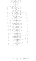
- Fig. 3 is a flow chart showing a known process of the waveform equalization.
- the generation of the clock signal is conducted independently of the waveform equalization.
- the received TV signal is fed to the transversal filter at the timing controlled by the clock signal from the clock circuit. This will not imply that the timing for resampling is optimum to the waveform equalization.
- the clock signal for resampling is being shifted in phase by application of a correction data from the outside to the PLL circuit, the waveform equalization has to be in no operation until the phase correction is completed thus increasing the entire processing time.
- the signal-to-noise (S/N) ratio has to be improved by repeating addition of the reference signals in the TV signal at equal intervals of time (as will be referred to as synchronous addition hereinafter). If the received TV signal contains noises of considerable levels which have not been attenuated, its waveform will hardly be distinguished from the original shape thus degrading the waveform equalization and, if worse, diverging the transmission system.
- the synchronous addition is needed upon every correction of the tap coefficients of the transversal filter thus increasing the overall time needed for the waveform equalization.
- a reference signal superimposed on the television signal is fed through a second memory to a central processing unit (referred to as a CPU hereinafter) and processed by synchronous addition to be a training signal.
- the training signal is then transferred to a first memory for storage and when requested, supplied alternative to the television signal to a transversal filter.
- the input and output training signals of the transmission filter are fed through the second memory to the CPU for waveform equalization.
- the CPU extracts a resampled phase value from the reference signal during producing the training signal, compares the resampled phase value with an ideal reference phase value to produce a phase difference, and sends a control voltage representing the phase difference to a PLL circuit which reproduces a clock signal from the television signal. Accordingly, the clock signal will be specified to produce optimum resampling phase matching in the waveform equalization.
- Fig. 1 illustrates a circuit diagram of a waveform equalizing system of the present invention, which comprises an A/D converter 1, a phase comparator 2, an adder 3, a D/A converter 4, a loop filter 5, a voltage controlled oscillator circuit 6, a first selector circuit 7, a second selector circuit 8, a transversal filter 9, a first memory 10, two second memories 11a and 11b, and a CPU 12.
- An input television signal is quantized by the A/D converter 1 and transmitted to the phase comparator circuit 2.
- the phase comparator circuit 2 detects a phase difference or delay between a horizontal synchronizing signal of the input TV signal and an output of the voltage controlled oscillator circuit 6 and delivers its corresponding voltage to the adder 3.
- the phase different voltage is added to a phase control signal fed from the CPU 12 which is adapted to control the transversal filter 9.
- the output of the adder 3 is converted by the D/A converter 4 to its analog equivalent which is then transmitted across the loop filter 5 to the voltage controlled oscillator circuit 6 for controlling the frequency of oscillation.
- the output of the voltage controlled oscillator circuit 6 is a reproduced clock signal and supplied to the A/D converter 1.
- the television signal after quantized is fed to the first selector circuit 7.
- the CPU 12 controls the first selector circuit 7 to open the "a" position to pass the TV signal to the transversal filter 9.
- the CPU 12 extracts VIT components of the TV signal at both input and output ends of the transversal filter 9 and takes them through the two memories 11a, 11b respectively for synchronous addition. Through repeating this action accompanied with the synchronous addition, the S/N ratio will be improved.
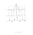
- Fig. 4(a) illustrates the resampling of an ideal VIT signal
- Fig. 4(b) shows a reproduction of the VIT signal through correct phase resampling
- Fig. 4(c) shows a phase deviated reproduction of the VIT signal created by erroneous resampling.
- the VIT signal extracted and subjected to synchronous addition by the CPU 12 has a waveform as shown in Fig. 4(c).
- the phase control signal supplied from the CPU 12 to the adder 3 is a data having a specified number of bits (e.g. a 4-bit signal), and a phase difference corresponding to one LSB (least significant bit) of the control signal is 1.5 nsec.
- the CPU 12 is provided with a table containing the values of theoretical VIT signals having phase differences of 1.5 nanoseconds unit and performs a correlation calculation from the theoretical values in the table and the values of the actually retrieved VIT signal. In the correlation calculation, local peaks in several cycles near the peak of the VIT signal are also involved for minimizing a calculation error resulted from noises at a low S/N ratio.
- a theoretical VIT signal which exhibits the largest correlative effect will be designated as the best match to the actual VIT signal, considering that its phase difference represents a phase distortion of the resampled signal. Accordingly, a reverse of the phase difference (the same in absolute value as and opposite in sign to the phase difference) is fed as the phase control signal to the adder 3.
- the transmission characteristics are identified from the reference signal in the TV signal, optimum resampling in the waveform equalization can be achieved by controlling the timing of resampling with the reference signal. Also, the use of the reference signal for the waveform equalization allows the synchronous addition to be assigned for common use. Accordingly, the overall time needed for the waveform equalization will be reduced as compared with a separate control over the timing for resampling.
- Fig. 2 is a flow chart showing a process of the waveform equalization.
- the VIT signal is extracted (Step 22) and processed by synchronous addition (Step 23) before moving to Step 25 because both steps are essential for both the waveform equalization and the resampling phase correction.
- Step 25 for resampling phase correction is completed, two Steps 22,23 for VIT signal extraction and synchronous addition are repeated. This repetitive action is accomplished by adding a new VIT signal to the resultant sum signal produced at Step 25.
- the VIT signal is transferred by the CPU 12 to the memory 10 where it is stored as a training signal.
- the selector circuit 7 is then switched to the "b" position for feeding the training signal of the memory 10 to the transversal filter 9.
- the CPU 12 extracts the training signals at the input and output of the transversal filter 9 through the respective memories 11a, 11b and compares them with the ideal reference signal form to produce differences which represent waveform distortions (Step 26).
- the tap coefficients of the transversal filter 9 are then calculated to desired values for attenuating the waveform distortions to zero (Step 27).
- the existing tap coefficients of the transversal filter 9 are replaced with the desired values (Step 28).
- the two steps 26 and 27 are repeated until the waveform distortions are completely eliminated.
- a series of Steps 26, 27, 28 for the waveform distortion detection, the tap coefficient calculation, and the tap coefficient correction can be conducted without involvement of previous Steps 22, 23 of the VIT signal extraction and the synchronous addition. Hence, the time consumption of this part of the sequence will be decreased considerably.
- the CPU 12 turns the selector circuit 7 from the "b" position to the "a” position and also, the selector circuit 8 from the "c" position to the "d” position for delivering a corrected waveform of the TV signal.
- the waveform distortions of the TV signal are compared by the CPU 12 before and after the waveform equalization to examine a change thereof (Step 30). If the change in the waveform distortion is found (Step 31) and its value is small (Step 32), the procedure starts again after Step 25 of the resampling phase correction. The procedure can however be minimized in time consumption similarly and thus, the traceability to waveform distortion change will be increased.
- the waveform equalization with the training signal is done in a closed loop. Accordingly, it can be conducted without being disturbed by a succeeding input of the TV signal and will thus remain stable and free from interference.
- Fig. 5 is a circuit diagram of another waveform equalizing system according to the present invention. Common components will be no more explained in details.
- the input TV signal is fed for generation of the clock signal to the PLL circuit which comprises a phase comparator circuit 2, an adder 3, a D/A converter 4, a loop filter 5, and a voltage controlled oscillator 6.
- the CPU 12 calculates several VIT signals which are lagged by several given values of ⁇ ⁇ in phase from the ideal VIT signal and sends them to a resampled phase delay detector circuit 13.
- the resampled phase delay detector circuit 13 then examines the correlation between the input TV signal and the VIT signal having a phase delay and fed from the CPU 12 and transfers back its result to the CPU 12. The correlation is examined on the plurality of VIT signals.
- the correlation is greater than a predetermined threshold value, it is judged that the VIT signal is deviated by ⁇ ⁇ in the phase at resampling. In consequence, a reverse of the characteristic of the VIT signal is assigned to the tap coefficient of the transversal filter 12. Then, the waveform equalization is carried out to eliminate waveform distortions derived from other than the resampled phase delay. As the waveform equalization is performed after the elimination of waveform distortions caused by the resampled phase delay, the time needed for convergence will be shortened.
- Fig. 6 is a circuit diagram of a further waveform equalizing system according to the present invention. Common components will be no more explained in details.
- An A/D converter 1 is provided for quantizing the clamp level component of the input TV signal to a given value.
- the clamp level components of the TV signal are fed through second memories 11a, 11b to a CPU 12 where they are compared with reference values contained. If the clamp level is different from the reference value, it is judged that the A/D converter 1 produced a quantizing error.
- the CPU 12 then demands a quantizing error correcting circuit 14 to correct the quantizing error. Succeedingly, the waveform equalization is carried out. No quantizing errors are involved after the quantizing error correction and the waveform equalization may thus be performed to eliminate inherent waveform distortions.
- Fig. 7 is a circuit diagram of a still further waveform equalizing system according to the present invention. Also, common components will be no more explained in details. There is not provided a means for detecting a change in the input TV signal because the TV signal is not fed to the CPU 12 during action of the waveform equalization with the training signal supplied via the "b" position of the selector circuit 7 from the memory 10. In particular, a waveform distortion change detector circuit 15 is provided for actuating independently of the waveform equalization to examine whether the waveform distortion is varied or not due to a change in the TV signal.
- the CPU 12 switches the selector circuit 7 from the "b" position to the "a” position and also, another selector circuit 8 from the "c" position to the "d” position for delivery of a waveform equalized version of the TV signal.
- This system will allow the waveform equalized signal to be passed steadily without being affected by any change in the waveform distortion.
- the input TV signal varies significantly after completion of the waveform equalization, it should be corrected by starting again the same process from initialization of the transversal filter. If its change is small, the waveform equalization may be continued to a succeeding cycle. However, the signal processing becomes interrupted in both cases thus producing a TV signal error for an instant.
- a modified arrangement of the CPU 12 contains a software or program of a digital filter equivalent to the transversal filter so as to carry out the waveform equalization without affecting the transversal filter 9. After completion of the waveform equalization by the equivalent digital filter, the characteristics of the transversal filter 9 is corrected. As the result, such TV signal error will be prevented.
- each resampled phase delay which has been detected is true or not.
- the examination can be made by comparing the phase of the present VIT signal with those of at least two, preceding and succeeding, VIT signal.
- the two other VIT signals have to be extracted in the same manner as of the present VIT component. Therefore, the CPU 12 is provided with a set of impulse responses of their respective resampled phase values and performs another resampling phase correction through multiplying the resampled phase by its preceding and succeeding impulse responses. Accordingly, the examination for the resampled phase delay will be done without extracting the comparative VIT signals.
Landscapes
- Engineering & Computer Science (AREA)
- Multimedia (AREA)
- Signal Processing (AREA)
- Picture Signal Circuits (AREA)
Applications Claiming Priority (4)
| Application Number | Priority Date | Filing Date | Title |
|---|---|---|---|
| JP121679/92 | 1992-05-14 | ||
| JP4121679A JPH05316391A (ja) | 1992-05-14 | 1992-05-14 | 波形等化装置 |
| JP4121624A JPH05316475A (ja) | 1992-05-14 | 1992-05-14 | ハイビジョン受像機 |
| JP121624/92 | 1992-05-14 |
Publications (2)
| Publication Number | Publication Date |
|---|---|
| EP0570190A2 true EP0570190A2 (fr) | 1993-11-18 |
| EP0570190A3 EP0570190A3 (en) | 1994-07-06 |
Family
ID=26458934
Family Applications (1)
| Application Number | Title | Priority Date | Filing Date |
|---|---|---|---|
| EP19930303627 Withdrawn EP0570190A3 (en) | 1992-05-14 | 1993-05-11 | Waveform equalizing system |
Country Status (2)
| Country | Link |
|---|---|
| US (1) | US5353069A (fr) |
| EP (1) | EP0570190A3 (fr) |
Families Citing this family (4)
| Publication number | Priority date | Publication date | Assignee | Title |
|---|---|---|---|---|
| JP3281992B2 (ja) * | 1993-03-26 | 2002-05-13 | 日本テキサス・インスツルメンツ株式会社 | ノイズ低減回路 |
| KR100238284B1 (ko) * | 1997-05-12 | 2000-01-15 | 윤종용 | 위상 보정 회로 및 그 방법 |
| US6515713B1 (en) * | 1998-12-31 | 2003-02-04 | Lg Electronics Inc. | Method and apparatus which compensates for channel distortion |
| JP3727206B2 (ja) * | 1999-11-11 | 2005-12-14 | Necエレクトロニクス株式会社 | クロック乗換回路及びその方法 |
Family Cites Families (5)
| Publication number | Priority date | Publication date | Assignee | Title |
|---|---|---|---|---|
| EP0179948B1 (fr) * | 1984-11-02 | 1988-05-25 | Deutsche ITT Industries GmbH | Récepteur de télévision en couleur comportant au moins un circuit intégré pour traiter le signal complet en couleurs numérisé |
| EP0212839B2 (fr) * | 1985-07-16 | 1994-10-19 | Matsushita Electric Industrial Co., Ltd. | Système de transmission/réception d'un signal de référence pour la suppression d'image fantôme |
| JPH0767167B2 (ja) * | 1989-01-20 | 1995-07-19 | 日本ビクター株式会社 | 波形等化器 |
| US5099328A (en) * | 1989-12-12 | 1992-03-24 | Matsushita Electric Industrial Co., Ltd. | Ghost canceller |
| JPH04103267A (ja) * | 1990-08-22 | 1992-04-06 | Matsushita Electric Ind Co Ltd | ゴースト除去装置 |
-
1993
- 1993-05-11 EP EP19930303627 patent/EP0570190A3/en not_active Withdrawn
- 1993-05-11 US US08/059,266 patent/US5353069A/en not_active Expired - Fee Related
Also Published As
| Publication number | Publication date |
|---|---|
| EP0570190A3 (en) | 1994-07-06 |
| US5353069A (en) | 1994-10-04 |
Similar Documents
| Publication | Publication Date | Title |
|---|---|---|
| JP4845246B2 (ja) | トレーニングモードを有する適応チャネル等化器 | |
| US20020051087A1 (en) | Repetitive-PN1023-sequence echo-cancellation reference signal for single-carrier digital television broadcast systems | |
| JPS61198848A (ja) | デ−タ受信システム | |
| KR0153610B1 (ko) | 영상 캐리어와 직각 위상을 이루는 캐리어를 변조한 신호에서의 고스트 억압 장치 | |
| US5159609A (en) | Data receiving device with delayed equalization and retroactive time-pulse recovery | |
| KR100337097B1 (ko) | 타이밍수단을포함하는전송시스템및수신기 | |
| US6570916B1 (en) | Adaptive equalization circuit and method | |
| EP0308776B1 (fr) | Egaliseur décodeur | |
| US5353069A (en) | Transmitted television signal waveform equalizing system | |
| JP2843690B2 (ja) | 波形等化回路 | |
| US5252932A (en) | Waveform equalizing filter unit | |
| EP0561556B1 (fr) | Egaliseur de signal vidéo | |
| JP2000244777A (ja) | 波形等化装置 | |
| JPH0345591B2 (fr) | ||
| JP2568765B2 (ja) | 波形等化装置 | |
| JPS62292079A (ja) | 自動波形等化器 | |
| Pazarci | An adaptive ghost processor for broadcast television | |
| JPH09135402A (ja) | 波形等化装置 | |
| JP2579090B2 (ja) | ハイビジョン受像機 | |
| US5347316A (en) | Image information transmission system having time base variation correcting function | |
| JPH05145793A (ja) | ハイビジヨン受像機 | |
| JPH06164982A (ja) | 波形等化装置 | |
| JPH0614626B2 (ja) | 自動波形等化器 | |
| KR950001506B1 (ko) | 자동 위상 등화 장치 | |
| JP2901645B2 (ja) | 波形等化回路 |
Legal Events
| Date | Code | Title | Description |
|---|---|---|---|
| PUAI | Public reference made under article 153(3) epc to a published international application that has entered the european phase |
Free format text: ORIGINAL CODE: 0009012 |
|
| AK | Designated contracting states |
Kind code of ref document: A2 Designated state(s): DE FR GB NL |
|
| PUAL | Search report despatched |
Free format text: ORIGINAL CODE: 0009013 |
|
| AK | Designated contracting states |
Kind code of ref document: A3 Designated state(s): DE FR GB NL |
|
| 17P | Request for examination filed |
Effective date: 19940812 |
|
| 17Q | First examination report despatched |
Effective date: 19960207 |
|
| STAA | Information on the status of an ep patent application or granted ep patent |
Free format text: STATUS: THE APPLICATION IS DEEMED TO BE WITHDRAWN |
|
| 18D | Application deemed to be withdrawn |
Effective date: 19980422 |