EP0570708A2 - Dispositifs de mémoire à lignes de bit ouvertes et méthode d'opération - Google Patents
Dispositifs de mémoire à lignes de bit ouvertes et méthode d'opération Download PDFInfo
- Publication number
- EP0570708A2 EP0570708A2 EP93106490A EP93106490A EP0570708A2 EP 0570708 A2 EP0570708 A2 EP 0570708A2 EP 93106490 A EP93106490 A EP 93106490A EP 93106490 A EP93106490 A EP 93106490A EP 0570708 A2 EP0570708 A2 EP 0570708A2
- Authority
- EP
- European Patent Office
- Prior art keywords
- bit line
- signal
- reference voltage
- memory
- sense amplifier
- Prior art date
- Legal status (The legal status is an assumption and is not a legal conclusion. Google has not performed a legal analysis and makes no representation as to the accuracy of the status listed.)
- Withdrawn
Links
Images

Classifications
-
- G—PHYSICS
- G11—INFORMATION STORAGE
- G11C—STATIC STORES
- G11C7/00—Arrangements for writing information into, or reading information out from, a digital store
- G11C7/18—Bit line organisation; Bit line lay-out
-
- G—PHYSICS
- G11—INFORMATION STORAGE
- G11C—STATIC STORES
- G11C11/00—Digital stores characterised by the use of particular electric or magnetic storage elements; Storage elements therefor
- G11C11/21—Digital stores characterised by the use of particular electric or magnetic storage elements; Storage elements therefor using electric elements
- G11C11/34—Digital stores characterised by the use of particular electric or magnetic storage elements; Storage elements therefor using electric elements using semiconductor devices
- G11C11/40—Digital stores characterised by the use of particular electric or magnetic storage elements; Storage elements therefor using electric elements using semiconductor devices using transistors
- G11C11/401—Digital stores characterised by the use of particular electric or magnetic storage elements; Storage elements therefor using electric elements using semiconductor devices using transistors forming cells needing refreshing or charge regeneration, i.e. dynamic cells
- G11C11/4063—Auxiliary circuits, e.g. for addressing, decoding, driving, writing, sensing or timing
- G11C11/407—Auxiliary circuits, e.g. for addressing, decoding, driving, writing, sensing or timing for memory cells of the field-effect type
- G11C11/409—Read-write [R-W] circuits
- G11C11/4091—Sense or sense/refresh amplifiers, or associated sense circuitry, e.g. for coupled bit-line precharging, equalising or isolating
-
- G—PHYSICS
- G11—INFORMATION STORAGE
- G11C—STATIC STORES
- G11C7/00—Arrangements for writing information into, or reading information out from, a digital store
- G11C7/06—Sense amplifiers; Associated circuits, e.g. timing or triggering circuits
Definitions
- This invention relates in general to semiconductor memory devices and to their operation, and more particularly, to dynamic random access memory (DRAM) devices configured with a novel open bit line architecture and to an operational method thereof.
- DRAM dynamic random access memory
- open bit line architecture In comparison with folded bit line architecture, open bit line architecture is more suitable for very close packing of memory cell arrays. Notwithstanding this, product chips using conventional open bit line cell arrays are rarely implemented, primarily because common mode noise reduction inherent in folded bit line architecture is lacking in open bit line architecture, at least without significant additional process complexity, signal loss and/or performance degradation. In view of the continuing advancement in the art towards greater and greater circuit integration, the open bit line configuration is drawing significant attention throughout the memory industry, especially in relation to 16 Mbit, 64 Mbit, and beyond, memories. This is because an open bit line architecture provides a memory cell at every X,Y cross-point location of the array, which is not possible with folded bit line architecture.
- Folded bit line architecture (commonly used in DRAMs of, for example, 256 Kbits or 1 Mbits) is inherently limited by the degree of integration obtainable within a defined area. Since a folded memory array cannot accommodate disposition of a memory cell at each bit line, word line intersection (i.e., cross-point), the configuration is by necessity less dense than an open bit line memory structure. By way of example, folded bit line architecture typically requires twenty-five percent, or more, area than open bit line architecture to implement the same size memory array. Thus, in terms of density of structure, an open bit line configuration clearly has the advantage. However, common mode noise difficulties inherent in conventional open bit line architectures have limited its commercial manufacture.
- the reference bit line which in a folded architecture supplies common-mode noise rejection, is for open bit line architecture either a parasitic capacitance liability or a source of additional noise.
- the present invention comprises in one aspect a novel open bit line memory device wherein at least some of the memory cells are interconnected by a bit line such that the bit line is able to perform selection of the interconnected memory cells.
- a signal detection unit is coupled to the bit line for sensing a developing signal on the line during a predefined bit line signal development interval.
- the detection unit also includes setting means for producing a signal having one of two logic states.
- the setting means operates during a predefined setting interval, which is subsequent the bit line signal development interval.
- this open bit line device includes an isolator for electrically separating the bit line from the signal detection unit for at least a portion of the unit's setting interval so that noise variations on the bit line during the setting interval do not effect the signal detection unit.
- the invention comprises a dynamic random access memory device which includes a plurality of memory cells arranged in a novel open bit line architecture. At least some of the memory cells are interconnected by a bit line, which functions to select the interconnected memory cells. Selection means for identifying a particular one of the interconnected memory cells to be read is also provided.
- a reference voltage line is associated with the bit line for providing a predefined reference voltage signal.
- a sense amplifier is coupled to the bit line for sensing a developing signal on the line from the selected one of the plurality of interconnected memory cells during a predefined bit line signal development period. Also coupled to the amplifier is the reference voltage line associated with the subject bit line.
- the amplifier includes a setting means for producing one of two logic states based upon a determined differential between a sensed signal on the bit line and the reference voltage signal.
- the sense amplifier produces its set signal during a predefined setting interval.
- an isolator is coupled to both the bit line and the associated reference voltage line for electrically isolating the lines from the sense amplifier for at least a portion of the sense amplifier's setting period so that signal variations on the lines are isolated from the sense amplifier for that portion of its setting interval.
- the present invention comprises a memory cell reading method for an open bit line memory device having a plurality of memory cells arranged in rows and columns.
- the open bit line device includes a plurality of periodically spaced bit lines for performing column selection of memory cells and a plurality of periodically spaced word lines for performing row selection of memory cells.
- the method includes the steps of: allowing a signal to develop on one of the plurality of bit lines representative of the state of a selected one of the memory cells interconnected by the subject bit line; utilizing a sensing device to read the signal on the selected bit line during a predefined bit line signal development period; electrically isolating the selected bit line from the sensing device; and at least partially simultaneous with the isolating step, producing a signal having one of two logical states based upon the signal developed on the selected bit line.
- the at least partial isolation step allows the signal produced by the sensing device to be defined at least partially independent of any continuing signal variations on the selected bit line.
- a novel open bit line DRAM device which is dense, requires no additional wiring levels, and is also easily laid out, is provided herein.
- the sense amplifier connection layout is similar to that of a folded sense amplifier layout. However, no reference bit line cells are required and no noise generated on a selected bit line (and associated reference voltage line) is passed to the sense amplifier while the sense amplifier is setting.
- the architecture presented allows for easy access of all array bits in a block-type layout with no special layout requirements on array edges. Improved sense amplifier setting performance is obtained through the light loading of internal sense amplifier nodes during the setting interval. Therefore, the sense amplifier can set rail to rail very quickly. Thus, bit switch timing can also be increased with faster driving of the data lines and I/O path.
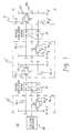
- FIG. 1 A conventional interleaved open bit line architecture, generally denoted 10, is depicted in FIG. 1.
- Arrangement 10 which is assumed to comprise a DRAM structure, includes multiple arrays 11 of memory cells (not shown). To reduce signal noise, each array 11 is typically disposed within a unique array well in a supporting substrate (not shown).
- Open bit line arrangement 10 also includes multiple sense amplifier banks, each of which contains multiple sense amplifier units 12.
- Each unit 12 is coupled to receive signals from a paired set of bit lines (such as BL1, BL1'; BL2, BL2'; BLi, BLi'; & BLj, BLj') on opposite sides of the respective sense amplifier bank.
- the true and complement (or reference) bit line pairings for this conventional open bit line configuration are on opposite sides of the corresponding sense amplifier unit 12.
- the bit switch “BS” gate line (shown in phantom) runs parallel to the various bit lines but on a second wiring level.
- Line “BS” connects selected bit lines to the appropriate data line bus, i.e., data line “DLi”, “DLj” or complementary data line “DL(C)i”, “DL(C)j”.
- Selection occurs through data output control transistors 14 (e.g., T1, T3, Ti, Tj), each of which is responsive to a unique control signal generated by a column decode circuit 16, and each of which is coupled between a data line bus and an adjacent sense amplifier bank.
- the transistors comprise n channel field effect transistors (NFETs) which are represented by a rectangle having a control element or gate electrode arranged adjacent thereto.
- circuits provided herein could be implemented with p channel field effect transistors (PFETs).
- PFETs p channel field effect transistors
- memory cells (not shown) are assumed to be disposed at every bit line, word line intersection (i.e., at every X,Y cross- point) in each array 11. Further, it is assumed that there are multiple bit line pairings coupled to each sense amplifier bank.
- conventional open bit line architecture such as arrangement 10, has a number of inherent problems.
- the arrangement requires a second wiring level to accommodate a bit switch gate line "BS" which, besides increasing manufacturing complexity, results in additional bit line parasitic capacitance.
- BS bit switch gate line
- edge array cells it is difficult to utilize edge array cells in a conventional open bit line architecture.
- array well voltage bounce under a selected bit line and/or reference bit line array can comprise a significant source of unbalanced noise between paired inputs to a sense amplifier unit.
- a common problem addressed by many open bit line architectures is how to deal with the reference bit line, which is typically either a parasitic capacitance liability or a source of additional noise.
- a significant feature to the architecture disclosed herein is the elimination of the reference bit line as heretofore known in the art. This reference line elimination is accomplished without compromising sense amplifier balance.
- the architecture disclosed herein utilizes a reference voltage signal in association with each bit line of a modified open bit line array.
- Bit lines are configured in an open cell architecture (i.e., a memory cell is disposed at each X,Y cross-point in the array) while common mode noise is able to be inherently reduced in a manner similar to that of folded bit line architecture.
- Common mode noise reduction is possible pursuant to the present invention because each bit line and its associated reference bit line are no longer in different array wells on opposite sides of the corresponding sense amplifier unit. Rather, each bit line is associated with a drastically truncated reference voltage line, and both are disposed on the same side of a sense amplifier unit.
- the architecture is more analogous to a folded bit line configuration.
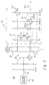
- FIG. 2 depicts one embodiment of a memory device, generally denoted 20, pursuant to the present invention.
- device 20 comprises a switched-gate isolation device which allows a folded sense amplifier layout to operate within a novel open bit line architecture.
- open bit line architecture is used herein to refer to a memory device having memory cells disposed at substantially every X,Y cross-point location in the memory array.
- open bit line architecture is used herein to refer to a memory device having memory cells disposed at substantially every X,Y cross-point location in the memory array.
- open bit line architecture is used herein to refer to a memory device having memory cells disposed at substantially every X,Y cross-point location in the memory array.
- a full reference bit line e.g., in a folded bit line array configuration
- the reference voltage line of the present invention is thus a vestigial portion of a conventional reference bit line cell.
- the memory cells (again, not shown) to be selected for reading by one or more sense amplifier units 22 in the depicted sense amplifier bank are disposed in a single array 23 to the right of the amplifier bank.
- One or more mirror image sense amplifier bank(s), memory array(s) and connecting structures could further exist to the right of the structures shown.
- every other bit line in array 23 is coupled to a different one of two sense amplifier banks disposed on opposite sides of the respective memory array, with each bit line (e.g. BL5 & BL6) terminating before reaching the other of the two opposing sense amplifier banks.
- reference voltage circuit 21 is positioned between the termination of the bit line and the sense amplifier bank to which the bit line is not coupled.
- Circuit 21 includes a reference voltage line, e.g., RVL5, and a reference voltage generator (not shown).
- the reference voltage generator produces a preselected voltage, such as the depicted 1/2 VDD, in part for input to the sense amplifier unit 22 coupled thereto.
- an isolation device is disposed, such as a switched-gate isolation transistor T5.
- Transistor T5 is gated “G” by an appropriately timed bit line isolation signal “BL(ISO),” and has its drain “D” connected to line BL5 and source “S” connected to unit 22.
- a reference isolation device such as a switched-gate reference transistor T6, is disposed to isolate a reference voltage generator (not shown) from sense amplifier unit 22 when active.
- Transistor T6 is gated “G” by an appropriately timed control signal "REF(ISO)” and has a source “S” coupled to the reference generator (which, e.g., supplies a 1/2 VDD signal), and a drain “D” connected to unit 22.
- isolation devices T5 & T6 When both NFET isolation transistors T5 & T6 are active, the bit line “BL” and the truncated reference line “RVL” are each connected directly to the sense amplifier unit. Again, isolation devices T5 & T6 are shown to comprise NMOS transistors, however, any alternate signal isolation means could be used.
- a first embodiment of a charge equalization circuit, denoted 24, is also depicted in FIG. 2.
- Sense amplifier units 22 set based on a determined differential between the signal on the respective bit line (e.g., BL5) in comparison with the signal on the corresponding reference voltage line (e.g., RVL5). Each unit 22 thus "reads" the value of the selected memory cell by setting to a high signal level or a low signal level based on the determined differential between signals on the associated bit and reference lines.
- bits input to each sense amplifier unit are typically equalized for a predetermined period of time. Subsequent equalization, the signal on the bit line is allowed to float to a higher or lower value. The change in the signal on the bit line is driven primarily by the state of the selected memory cell. This time interval during which the bit line floats is referred to as the "bit line signal development period or interval".
- the sense amplifier unit experiences a "setting interval" during which time the unit sets to either a high signal value or a low signal value based on the differential between the developed signal on the bit line and the reference voltage signal, which will remain relatively constant, i.e., assuming that the bit line and reference voltage line are equalized at the reference signal voltage.
- the bit line and its truncated reference voltage line are returned to an equalized state.
- FIG. 2 also depicts one possible embodiment of circuitry, labeled 24, to accomplish equalization between the lines.
- Equalization circuit 24 utilizes two serially connected transistors T10 & T11 disposed between the bit line BL5 and its associated reference voltage line RVL5. Each transistor T10 & T11 is gated “G” by an equalization control signal “EQ”.
- the drain “D” of transistor T10 is connected to bit line BL5, while its source “S” is coupled to the drain “D” of transistor T11.
- the common node connection between transistors T10 & T11 is also connected to an equalization voltage supply line "V(EQ)", which by way of example may comprise a 1/2 VDD signal.
- the source “S” of transistor T11 is connected to reference voltage line RVL5.
- data is read out from amplifier unit 22 to either a true data line bus “DL” or a complementary data line bus “DL(C)” through switching transistors T12 & T13, which are gated “G” by a signal from a column decode circuit 25.
- Transistor T12 is connected between unit 22 and data line bus “DL” such that its drain “D” is connected to the data line and its source “S” connects to the sense amplifier unit.
- transistor T13 has its drain “D” connected to the sense amplifier unit and its source “S” wired to the complementary data bus line "DL(C)".
- the row address strobe (RAS) is inactive, 40 "RAS Inactive.”
- signals "EQ”, “BL(ISO)”, and “REF(ISO)” are high, the bit switch signal “BS” from the column decode circuit and the appropriate array word line are low, and the equalization voltage "V(EQ)" is at a predefined level, e.g., one-half VDD.
- a cycle starts, 42 "Cycle Start” (e.g., RAS Falls), and a word line is selected, 44 "Word Line Select.”
- a charge is then transferred into the internal node of the sense amplifier from the connected bit line while the bit line floats, 46 "Bit Lines Float; Charge Transferred to Sense Amplifier.”
- the sense amplifier is isolated, e.g., by dropping "BL(ISO)” and “REF(ISO)” low, 48 "Sense Amplifier Isolation”.
- the amplifier sets using the signals developed at its internal nodes, 50 "Sense Amplifier Sets.” Because of this amplifier isolation, the values to the input of the sense amplifier are frozen and the sense amplifier is independent of any signal variations on the bit line and/or reference line.
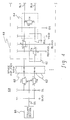
- FIG. 4 depicts an alternate embodiment of an open bit line architecture pursuant to the present invention.
- This memory device generally denoted 60, includes a memory array 63 having a plurality of memory cells (not shown) arranged in rows and columns.
- a sense amplifier bank is disposed adjacent array 63 and includes a plurality of sense amplifier units 62.
- each paired input to a sense amplifier unit originates from the same array well on one side of the sense amplifier bank.
- Amplifier banks (only one of which is depicted) are disposed on opposing sides of memory array 63 and each bit line (e.g., BL7) is connected to only one sense amplifier bank. Again, each bit line is associated with a reference voltage line (e.g., RVL7).
- Circuit 61 comprises the reference voltage supply to the depicted sense amplifier unit 62.
- Gated isolation transistors T7 & T8 again control connection of bit line BL7 and reference voltage line RVL7, respectively, to amplifier unit 62.
- Transistors T7 & T8 are gated and connected in the same manner as transistors T5 & T6 (FIG. 2) described above, except transistor T8 has its source "S” connected to receive the equalization voltage "V(EQ)" rather than a separate reference voltage supply. (In effect, the equalization voltage "V(EQ)" and reference voltage signal are made equal.)
- Circuit 64 comprises a transistor T14, which in the embodiment depicted is an NFET gated “G” by the equalization "EQ” control signal. Transistor T14 has its drain “D” connected to bit line BL7 and its source “S” connected to the equalization voltage "V(EQ)".
- Data is read out from amplifier unit 62 in a manner similar to the process described above in connection with unit 22 of FIG. 2.
- the data output switching transistors are labeled T15 & T16, and are gated “G” by a bit switch "BS" signal from a column decode circuit 65.
- the device is dense, requires no additional wiring levels, and is easily laid out.
- the sense amplifier connection layout is similar to that of a folded sense amplifier layout.
- no reference bit line cells are required and no noise generated on a selected bit line and/or associated reference voltage line is passed to the sense amplifier while the sense amplifier is setting.
- the architecture presented allows for easy access of all array bits in a block-type layout with no special layout requirements on array edges. Improved sense amplifier setting performance is obtained through the light loading of internal sense amplifier nodes. Therefore, the sense amplifier can set rail to rail very quickly.
- bit switch timing can also be increased with faster driving of the data lines and I/O path.
Landscapes
- Engineering & Computer Science (AREA)
- Microelectronics & Electronic Packaging (AREA)
- Computer Hardware Design (AREA)
- Dram (AREA)
- Semiconductor Memories (AREA)
Applications Claiming Priority (2)
| Application Number | Priority Date | Filing Date | Title |
|---|---|---|---|
| US888226 | 1992-05-22 | ||
| US07/888,226 US5303196A (en) | 1992-05-22 | 1992-05-22 | Open bit line memory devices and operational method |
Publications (2)
| Publication Number | Publication Date |
|---|---|
| EP0570708A2 true EP0570708A2 (fr) | 1993-11-24 |
| EP0570708A3 EP0570708A3 (en) | 1994-06-01 |
Family
ID=25392788
Family Applications (1)
| Application Number | Title | Priority Date | Filing Date |
|---|---|---|---|
| EP19930106490 Withdrawn EP0570708A3 (en) | 1992-05-22 | 1993-04-21 | Open bit line memory devices and operational method |
Country Status (3)
| Country | Link |
|---|---|
| US (1) | US5303196A (fr) |
| EP (1) | EP0570708A3 (fr) |
| JP (1) | JPH0628843A (fr) |
Cited By (2)
| Publication number | Priority date | Publication date | Assignee | Title |
|---|---|---|---|---|
| WO2005073982A1 (fr) * | 2004-01-28 | 2005-08-11 | Koninklijke Philips Electronics N.V. | Dispositif a circuit integre comprenant une matrice rom |
| EP1298668A3 (fr) * | 2001-09-27 | 2006-10-04 | Kabushiki Kaisha Toshiba | Mémoire à semi-conducteur avec amplificateur de détection indépendant de l'horloge |
Families Citing this family (7)
| Publication number | Priority date | Publication date | Assignee | Title |
|---|---|---|---|---|
| JP3305449B2 (ja) * | 1993-09-17 | 2002-07-22 | 富士通株式会社 | 半導体記憶装置 |
| US5982693A (en) * | 1997-12-10 | 1999-11-09 | Programmable Microelectronics Corporation | Sense amplifier with improved bit line initialization |
| KR100388318B1 (ko) | 1998-12-24 | 2003-10-10 | 주식회사 하이닉스반도체 | 비트라인디커플링방법 |
| GB2354618B (en) * | 1999-09-24 | 2001-11-14 | Pixelfusion Ltd | Memory devices |
| US6301175B1 (en) | 2000-07-26 | 2001-10-09 | Micron Technology, Inc. | Memory device with single-ended sensing and low voltage pre-charge |
| US6292417B1 (en) | 2000-07-26 | 2001-09-18 | Micron Technology, Inc. | Memory device with reduced bit line pre-charge voltage |
| JP5007722B2 (ja) * | 2006-03-28 | 2012-08-22 | 富士通セミコンダクター株式会社 | 半導体メモリおよびシステム |
Family Cites Families (13)
| Publication number | Priority date | Publication date | Assignee | Title |
|---|---|---|---|---|
| JPS5939836B2 (ja) * | 1976-10-27 | 1984-09-26 | 日本電気株式会社 | 記憶集積回路 |
| JPS5931155B2 (ja) * | 1979-10-11 | 1984-07-31 | インターナシヨナルビジネス マシーンズ コーポレーシヨン | 感知増幅回路 |
| US4312047A (en) * | 1980-05-29 | 1982-01-19 | Motorola, Inc. | Memory array having improved isolation between sense lines |
| JPS5760589A (en) * | 1980-09-30 | 1982-04-12 | Nec Corp | Memory circuit |
| JPS57208691A (en) * | 1981-06-15 | 1982-12-21 | Mitsubishi Electric Corp | Semiconductor memory |
| US4701885A (en) * | 1984-07-26 | 1987-10-20 | Texas Instruments Incorporated | Dynamic memory array with quasi-folded bit lines |
| JPS61110459A (ja) * | 1984-11-02 | 1986-05-28 | Nippon Telegr & Teleph Corp <Ntt> | 半導体メモリ |
| US4733374A (en) * | 1985-03-30 | 1988-03-22 | Kabushiki Kaisha Toshiba | Dynamic semiconductor memory device |
| US4888732A (en) * | 1987-02-23 | 1989-12-19 | Matsushita Electric Industrial Co., Ltd. | Dynamic random access memory having open bit line architecture |
| JPS63206991A (ja) * | 1987-02-23 | 1988-08-26 | Matsushita Electric Ind Co Ltd | ダイナミツク型ram |
| JPS6413290A (en) * | 1987-07-07 | 1989-01-18 | Oki Electric Ind Co Ltd | Semiconductor memory |
| US4804871A (en) * | 1987-07-28 | 1989-02-14 | Advanced Micro Devices, Inc. | Bit-line isolated, CMOS sense amplifier |
| US4918663A (en) * | 1987-09-16 | 1990-04-17 | Motorola, Inc. | Latch-up control for a CMOS memory with a pumped well |
-
1992
- 1992-05-22 US US07/888,226 patent/US5303196A/en not_active Expired - Fee Related
-
1993
- 1993-04-20 JP JP5093076A patent/JPH0628843A/ja active Pending
- 1993-04-21 EP EP19930106490 patent/EP0570708A3/en not_active Withdrawn
Cited By (3)
| Publication number | Priority date | Publication date | Assignee | Title |
|---|---|---|---|---|
| EP1298668A3 (fr) * | 2001-09-27 | 2006-10-04 | Kabushiki Kaisha Toshiba | Mémoire à semi-conducteur avec amplificateur de détection indépendant de l'horloge |
| WO2005073982A1 (fr) * | 2004-01-28 | 2005-08-11 | Koninklijke Philips Electronics N.V. | Dispositif a circuit integre comprenant une matrice rom |
| US7554831B2 (en) | 2004-01-28 | 2009-06-30 | Nxp B.V. | Integrated circuit device with a ROM matrix |
Also Published As
| Publication number | Publication date |
|---|---|
| US5303196A (en) | 1994-04-12 |
| JPH0628843A (ja) | 1994-02-04 |
| EP0570708A3 (en) | 1994-06-01 |
Similar Documents
| Publication | Publication Date | Title |
|---|---|---|
| KR100329024B1 (ko) | 파괴 읽기형 메모리 회로, 이를 위한 리스토어 회로 및 감지 증폭기 | |
| US5367488A (en) | DRAM having bidirectional global bit lines | |
| KR100538883B1 (ko) | 반도체 메모리 장치 | |
| CA2217359C (fr) | Methode de detection pour dram multiniveau | |
| EP0264929B1 (fr) | Dispositif de mémoire à semi-conducteurs avec une disposition modifiée de lignes de bit | |
| US5850367A (en) | Static type semiconductor memory with latch circuit amplifying read data read on a sub bit line pair and transferring the amplified read data to a main bit line pair and operation method thereof | |
| US6023437A (en) | Semiconductor memory device capable of reducing a precharge time | |
| EP0920027B1 (fr) | Cellule de mémoire RAM à consommation réduite avec une seule ligne de bit | |
| KR100308842B1 (ko) | 반도체메모리 | |
| US5303196A (en) | Open bit line memory devices and operational method | |
| EP0834883B1 (fr) | Dispositif de mémoire à semi-conducteur non volatile | |
| JPH0467496A (ja) | 半導体メモリ | |
| US7286425B2 (en) | System and method for capacitive mis-match bit-line sensing | |
| US5359566A (en) | Dynamic random access memory | |
| US4602355A (en) | Memory circuit with noise preventing means for word lines | |
| EP0172112A2 (fr) | Dispositif de mémoire semi-conductrice | |
| US5862072A (en) | Memory array architecture and method for dynamic cell plate sensing | |
| JPH0411954B2 (fr) | ||
| EP0166642A2 (fr) | Dispositif semi-conducteur divisé en blocs avec lignes de bit divisées | |
| KR100344819B1 (ko) | 불휘발성 강유전체 메모리 장치 및 그 구동회로 | |
| JP3415420B2 (ja) | 半導体集積回路装置 | |
| WO1985002314A2 (fr) | Memoire a semi-conducteurs | |
| US5321647A (en) | Semiconductor memory device and operational method with reduced well noise | |
| US20020186607A1 (en) | Sense amplifier and architecture for open digit arrays | |
| US6434069B1 (en) | Two-phase charge-sharing data latch for memory circuit |
Legal Events
| Date | Code | Title | Description |
|---|---|---|---|
| PUAI | Public reference made under article 153(3) epc to a published international application that has entered the european phase |
Free format text: ORIGINAL CODE: 0009012 |
|
| AK | Designated contracting states |
Kind code of ref document: A2 Designated state(s): DE FR GB |
|
| PUAL | Search report despatched |
Free format text: ORIGINAL CODE: 0009013 |
|
| 17P | Request for examination filed |
Effective date: 19940324 |
|
| AK | Designated contracting states |
Kind code of ref document: A3 Designated state(s): DE FR GB |
|
| 18W | Application withdrawn |
Withdrawal date: 19960716 |