EP0570839A2 - Schaltungsanordnung zur Kompensation von Spannungsabfällen an Versorgungsleitungen bzw. zur Minderung der Oberwellen des Stromes - Google Patents
Schaltungsanordnung zur Kompensation von Spannungsabfällen an Versorgungsleitungen bzw. zur Minderung der Oberwellen des Stromes Download PDFInfo
- Publication number
- EP0570839A2 EP0570839A2 EP93107782A EP93107782A EP0570839A2 EP 0570839 A2 EP0570839 A2 EP 0570839A2 EP 93107782 A EP93107782 A EP 93107782A EP 93107782 A EP93107782 A EP 93107782A EP 0570839 A2 EP0570839 A2 EP 0570839A2
- Authority
- EP
- European Patent Office
- Prior art keywords
- phase
- supply network
- voltage
- switching matrix
- circuit arrangement
- Prior art date
- Legal status (The legal status is an assumption and is not a legal conclusion. Google has not performed a legal analysis and makes no representation as to the accuracy of the status listed.)
- Granted
Links
Images



Classifications
-
- G—PHYSICS
- G05—CONTROLLING; REGULATING
- G05F—SYSTEMS FOR REGULATING ELECTRIC OR MAGNETIC VARIABLES
- G05F1/00—Automatic systems in which deviations of an electric quantity from one or more predetermined values are detected at the output of the system and fed back to a device within the system to restore the detected quantity to its predetermined value or values, i.e. retroactive systems
- G05F1/10—Regulating voltage or current
- G05F1/12—Regulating voltage or current wherein the variable actually regulated by the final control device is AC
- G05F1/32—Regulating voltage or current wherein the variable actually regulated by the final control device is AC using magnetic devices having a controllable degree of saturation as final control devices
-
- H—ELECTRICITY
- H02—GENERATION; CONVERSION OR DISTRIBUTION OF ELECTRIC POWER
- H02J—ELECTRIC POWER NETWORKS; CIRCUIT ARRANGEMENTS OR SYSTEMS FOR SUPPLYING OR DISTRIBUTING ELECTRIC POWER; SYSTEMS FOR STORING ELECTRIC ENERGY
- H02J3/00—Circuit arrangements for AC mains or AC distribution networks
- H02J3/01—Arrangements for reducing harmonics or ripples
-
- H—ELECTRICITY
- H02—GENERATION; CONVERSION OR DISTRIBUTION OF ELECTRIC POWER
- H02J—ELECTRIC POWER NETWORKS; CIRCUIT ARRANGEMENTS OR SYSTEMS FOR SUPPLYING OR DISTRIBUTING ELECTRIC POWER; SYSTEMS FOR STORING ELECTRIC ENERGY
- H02J3/00—Circuit arrangements for AC mains or AC distribution networks
- H02J3/18—Arrangements for adjusting, eliminating or compensating reactive power in networks
- H02J3/1807—Arrangements for adjusting, eliminating or compensating reactive power in networks using series compensators, e.g. thyristor-controlled series capacitors [TCSC]
-
- H—ELECTRICITY
- H02—GENERATION; CONVERSION OR DISTRIBUTION OF ELECTRIC POWER
- H02M—APPARATUS FOR CONVERSION BETWEEN AC AND AC, BETWEEN AC AND DC, OR BETWEEN DC AND DC, AND FOR USE WITH MAINS OR SIMILAR POWER SUPPLY SYSTEMS; CONVERSION OF DC OR AC INPUT POWER INTO SURGE OUTPUT POWER; CONTROL OR REGULATION THEREOF
- H02M1/00—Details of apparatus for conversion
- H02M1/12—Arrangements for reducing harmonics from AC input or output
-
- Y—GENERAL TAGGING OF NEW TECHNOLOGICAL DEVELOPMENTS; GENERAL TAGGING OF CROSS-SECTIONAL TECHNOLOGIES SPANNING OVER SEVERAL SECTIONS OF THE IPC; TECHNICAL SUBJECTS COVERED BY FORMER USPC CROSS-REFERENCE ART COLLECTIONS [XRACs] AND DIGESTS
- Y02—TECHNOLOGIES OR APPLICATIONS FOR MITIGATION OR ADAPTATION AGAINST CLIMATE CHANGE
- Y02E—REDUCTION OF GREENHOUSE GAS [GHG] EMISSIONS, RELATED TO ENERGY GENERATION, TRANSMISSION OR DISTRIBUTION
- Y02E40/00—Technologies for an efficient electrical power generation, transmission or distribution
- Y02E40/30—Reactive power compensation
-
- Y—GENERAL TAGGING OF NEW TECHNOLOGICAL DEVELOPMENTS; GENERAL TAGGING OF CROSS-SECTIONAL TECHNOLOGIES SPANNING OVER SEVERAL SECTIONS OF THE IPC; TECHNICAL SUBJECTS COVERED BY FORMER USPC CROSS-REFERENCE ART COLLECTIONS [XRACs] AND DIGESTS
- Y02—TECHNOLOGIES OR APPLICATIONS FOR MITIGATION OR ADAPTATION AGAINST CLIMATE CHANGE
- Y02E—REDUCTION OF GREENHOUSE GAS [GHG] EMISSIONS, RELATED TO ENERGY GENERATION, TRANSMISSION OR DISTRIBUTION
- Y02E40/00—Technologies for an efficient electrical power generation, transmission or distribution
- Y02E40/40—Arrangements for reducing harmonics
Definitions
- the invention relates to a circuit arrangement for compensating voltage drops on supply lines or for reducing the harmonics of the current, in the terminals of an alternating current source via a supply network, which represents an impedance consisting of inductors and resistors, to the input of an electronic voltage and / or or current compensator are connected, a load impedance being connected to the output of the compensator.
- the voltage value at the consumers must correspond to the character of the consumer, adapted tolerances, otherwise the consumer cannot work according to his purpose.
- the mean or effective value of the voltage must generally be kept below the appropriate limits, but some consumers can only tolerate slow changes within the tolerances.
- a typical example of this is the supply of incandescent lamps, where rapid changes are only permitted with relatively low amplitudes.
- More sensitive electronic devices face increased demands on electrical energy supply. This can mean tighter voltage tolerances, and much more stringent requirements are also placed on transient voltage changes.
- the fundamental wave of the consumer current has a phase shift compared to the mains voltage (cos ⁇ ⁇ 1), and, on the other hand, that the consumer current contains harmonics of various orders in addition to its fundamental wave.
- Another method of compensating for the voltage drop is to insert a capacitor to the line in a series circuit (as is usual in long-distance lines with high operating voltages), or a transformer with its primary winding to the line in a series connection is inserted, the secondary winding of the same transformer being connected to a capacitor.
- the capacitor, or its capacitive reactance, which is reduced to the primary side can compensate the inductive reactance of the line if dimensioned accordingly.
- the disadvantage of this solution is that the voltage drop that occurs across the ohmic resistance of the line cannot be compensated for in this way, so that in order to reduce it, much larger line cross sections must be installed than would be necessary due to the thermal load-bearing capacity is often a very expensive measure.
- circuit arrangements can generally be characterized with an intricate design, with the use of numerous, expensive switching elements and the need for complicated control.
- the purpose of the invention is to develop a much simpler and therefore correspondingly more economical solution for compensating voltage drops.
- the invention is based on the following knowledge: if one inserts the primary winding of a transformer into the supply network in a series connection between the current source and the load, the secondary winding of the same transformer being connected by a switch between phase and zero of the supply network, then the switch is permanently closed a voltage corresponding to the step-up (step-down) of the transformer is added to the voltage of the supply network, however, with the switch permanently open, the inductance of the primary winding of the transformer is connected in series to the inductance of the supply network, so that the voltage at the load is lower than that of the supply network becomes.
- the voltage of the desired magnitude can always be produced at the load terminals. If the frequency of the switching operations is still selected 50 to 100 times higher (or even higher) than the frequency of the supply voltage, the voltage at the load terminals can follow a reference variable not only in the mean value or RMS value, but also within its period, i.e. practically normally sinusoidal stay.
- primary winding (s) of transformer (s) is / are inserted between phase output (s) of the supply network and load impedance, a feed line (s) for the (individual) secondary winding (s) to phase output (s) output (e ) of the supply network and other supply line (s) is / are connected directly or indirectly to the neutral point of the supply network via single-phase switching matrix (s), or are connected to one another via a three-phase switching matrix.
- the invention is further designed on the basis of the exemplary embodiments illustrated in the figures.
- the first illustration shows a circuit arrangement corresponding to an embodiment of the invention, for a single-phase supply network.
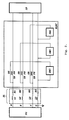
- the second figure shows another embodiment of the invention for a three-phase supply network.
- the third figure shows another embodiment of the invention, also for a three-phase supply network.
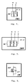
- the 4th figure shows an example of a single-phase switching matrix.
- the 5th figure shows an example of a three-phase switching matrix.
- the 6th figure shows an example of a switching element that was realized with a bipolar transistor insulated base (IGBT) and a diode connected in parallel to it.
- IGBT bipolar transistor insulated base
- the 7th, 8th and 9th figures show current and voltage profiles which characterize the functioning of a circuit arrangement according to the invention.
- the terminals 0, P1 of a single-phase power source are connected to the input terminals P2, P4 of the electronic voltage and / or current compensator ELDC via the supply network ZL.
- the resulting impedance of the supply network ZL is composed of the inductors L0, L1 and resistors R0, R1 of the same network ZL.
- the output terminals P3, P5 of the compensator ELDC are connected to the Leads of load impedance LD connected.
- the primary winding PR of the transformer TR in the compensator ELDC is connected between the input terminal P2 and the output terminal P3 of the same compensator ELDC, the secondary winding SR of the same transformer TR directly or via the filter circuit F and further via the single-phase switching matrix SM1 to the input terminal P4 of the compensator ELDC connected.
- the circuit arrangement according to Figure 1. can be operated in the manner described below:
- the consumer that is drawn with the impedance LD is supplied by the single-phase power source PS. Since a voltage drop occurs at the resulting impedance of the supply network ZL, the voltage present decreases from the output voltage V1 of the current source PS to the input terminals P2, P4 of the compensator ELDC to the voltage value V2.
- the basic function of the switching matrix SM1 corresponds to an idealized switch. According to the invention, the switching matrix SM1 is switched on and off at a frequency that is increased, for example 50 to 100 times higher than the fundamental wave of the current source PS.
- the temporal ratio of the switched on or switched off states and thus the relative pulse width PW is determined by an electronic control part belonging to the circuit arrangement corresponding to the desired output voltage V3.
- the inductance of the primary winding PR of the transformer TR is connected in series with the inductances L0, L1 of the supply network, so that the output voltage V3 becomes lower than the input voltage V2. This means that the voltage can not only be increased but also reduced with this circuit arrangement, which is of particular practical importance.
- the relative pulse width PW can be changed and the voltage V3 that appears at the consumer can be set exactly to a predetermined value. Since the switching frequency of the single-phase switching matrix SM1 is about two orders of magnitude higher than the frequency of the current source PS, in other words, since the single-phase switching matrix SM1 is switched 50 to 100 times within one period of the voltage of the current source PS, it can be achieved be that the voltage V3 not only has the desired mean or effective value, but also follows a predetermined command variable within each period, for example has sinusoidal waveform.
- the voltage induced in the primary winding PR of the transformer TR also has a high-frequency component which suppresses the switching frequency Need to become.
- This type of screening can be carried out either on the primary or on the secondary (possibly simultaneously on both) side (s).
- the screening is carried out with a filter circuit F connected in series with the secondary winding SR on the secondary side.
- the screening on the secondary side has the advantage that the transformer does not have to transmit a high-frequency component, so it can simply be designed for the fundamental waves of current and voltage.
- the required type power of the compensator ELDC is proportional to the extent of the desired compensation. Is e.g. only to compensate for voltage drop in the range of + -10%, the required type power of the compensator ELDC is about 10% of the consumer power.
- the supply lines R, S, T, 0 of the three-phase power source PS are via the supply network ZL, the impedance of which is described with the inductors L1, L2, L3, L0 and with the resistors R1, R2, R3, R0 , connected to the compensator ELDC.
- a primary winding of one of the three transformers TR is inserted into a series connection, the secondary windings SR of the transformers TR directly or indirectly via a filter circuit F and also via a single-phase switching matrix SM1 to the one grounded this time neutral line of the supply network ZL are connected.
- This circuit arrangement essentially contains three single-phase circuit arrangements. The functioning of the circuits belonging to the individual phases completely corresponds to the previous description.
- the voltages or the harmonic contents of the individual phases can be compensated for independently of one another, since the circuits belonging to the individual phases do not interact with one another.
- phase voltages can be compensated in the arrangement according to Figure 3 with the help of the three-phase switching matrix SM3, which contains only a single switching element.
- the single-phase switching matrix SM1 is shown in the fourth figure.
- This exemplary embodiment contains a bridge circuit consisting of diodes D1, D2, D3, D4, in the bridging branch of which there is a semiconductor switching element SW.
- the three-phase switching matrix SM3, which is shown in the 5th figure, contains a three-phase bridge circuit consisting of diodes D1, D2, D3, D4, D5, D6, in the bridging branch of which there is a semiconductor switching element SW.
- the 6th figure shows an embodiment of the semiconductor switching element SW, which consists of a bipolar transistor insulated base (IGBT) and a diode D7 connected between its emitter and collector.
- IGBT bipolar transistor insulated base
- the 7th, 8th and 9th figures show current and voltage curves obtained from computer simulation, in which the frequency of the fundamental wave is 400 Hz, the relative pulse width PW is 60% and the consumer power (in the three phases in total) is 60 kVA.
- the current of the single-phase switching matrix SM1 on the 8th figure the voltage difference V3-V2, and on the 9th figure the output voltage V3 is drawn.
- the frequency of the switching operations is 50 times the frequency of the fundamental wave. It can clearly be seen that the waveform of the output voltage V3 is close to the sinusoidal shape and the mean value of the same output voltage V3 corresponds to the desired mean value.
- the problem solution according to the invention results in a simple structure which can be controlled in a simple manner, and thereby enables the voltage of the consumers to be stabilized with its help and, if necessary, the harmonic content of the current to be compensated at the same time.
- the stabilization of the consumer voltage can not only mean the regulation of its mean or effective value, but also the correction of its distortions (deviations from the sinusoidal shape).
Landscapes
- Engineering & Computer Science (AREA)
- Power Engineering (AREA)
- Physics & Mathematics (AREA)
- Electromagnetism (AREA)
- General Physics & Mathematics (AREA)
- Radar, Positioning & Navigation (AREA)
- Automation & Control Theory (AREA)
- Ac-Ac Conversion (AREA)
Abstract

Description
- Die Erfindung bezieht sich auf eine Schaltungsanordnung zur Kompensation von Spannungsabfällen an Versorgungsleitungen bzw. zur Minderung der Oberwellen des Stromes, in der Klemmen einer Wechselstromquelle über ein Versorgungsnetzwerk, das eine aus Induktivitäten und Widerständen bestehende Impedanz darstellt, an den Eingang eines elektronischen Spannungs- und/oder Stromkompensators angeschlossen sind, wobei an den Ausgang des Kompensators eine Lastimpedanz angeschlossen ist.
- Wie es allgemein bekannt ist, bedeutet der Spannungsabfall, der an Beförderungsleitungen infolge des Stromes entsteht, bei der Beförderung und Verteilung der elektrischen Energie ein wesentliches praktisches Problem.
- Der Spannungswert an den Verbrauchern muß dem Charakter der Verbraucher angepassten Toleranzen entsprechen, sonst kann der Verbraucher nicht seiner Bestimmung entsprechend arbeiten. Für passive Verbraucher muss allgemein der Mittelwert oder Effektivwert der Spannung unter entsprechenden Grenzen gehalten werden, einige Verbraucher ertragen jedoch auch binnen der Toleranzen nur langsame Veränderungen. Ein typisches Beispiel dafür ist die Speisung von Glühlampen, wo schnelle Veränderungen nur mit verhältnismässig geringen Amplituden zulässig sind.
Empfindlichere elektronische Einrichtungen stellen erhöhte Anforderungen der elektrischen Energieversorgung gegenüber. Dies kann engere Spannungstoleranzen bedeuten, und auch den transienten Spannungsveränderungen gegenüber werden viel strengere Anforderungen gestellt. - Als weitere Probleme der elektrischen Energieverteilung sind festzustellen, einerseits, daß die Grundwelle des Verbraucherstromes eine phasenmäßige Verschiebung gegenüber der Netzspannung aufweist ( cos φ < 1 ), anderseits, daß der Verbraucherstrom neben seiner Grundwelle auch Oberwellen verschiedener Ordnung enthält.
- Geringe Werte des Leistungsfaktors und Stromoberwellen verursachen zusätzliche Verluste, und reduzieren damit die an einer vorhandenen Leitung übertragbare Leistung. Oberwellen des Stromes verzerren dabei noch die Wellenform der Verbraucherspannung, das bei elektronischen Verbrauchern Funktionsstörungen herbeiführen kann.
- In Netzwerken, die unter Spannungen höherer Frequenz (z.B. 400Hz) arbeiten, kann der Spannungsabfall an den Versorgungsleitungen zu ernsthaften Schwierigkeiten führen. In solchen Fällen kann die elektrische Energie auch über Kleinere Entfernungen nur mit Sonderkabel großen Querschnitts und komplizierter Konstruktion befördert werden, die eine sehr kostspielige Lösung darstellt.. ( Solche Systeme werden z.B. an Flughäfen betrieben.)
- Zur Kompensation der an den Leitungen entstehenden Spannungsabfälle sind verschiedene Lösungen erarbeitet geworden. Einrichtungen, die auf dem Prinzip der Ferroresonanz arbeiten, werden zum Beispiel seit mehreren Jahrzehnten eingesetzt. Diese Lösung hat den Nachteil, daß verhältnismäßig grosse reaktive Leistungen eingebaut werden müßen, sodaß sie für größere Leistungen kaum mehr gebraucht wird.
- Eine andere, auch in der heutigen Praxis häufig verwendete Methode der Kompensation des Spannungsabfalles besteht darin, daß ein Kondensator zu der Leitung in eine Reihenschaltung eingefügt wird (wie dies in Fernleitungen hoher Betreibsspannungen üblich ist), oder ein Transformator mit seiner Primärwicklung zu der Leitung in eine Reihenschaltung eingefügt wird, wobei die Sekundärwicklung desselben Transformators an einen Kondensator angeschlossen wird. So kann der Kondesator, bzw. seine auf die Primärseite reduzierte kapazitive Reaktanz bei entsprechender Bemessung die induktive Reaktanz der Leitung kompensieren. Der Nachteil dieser Lösung besteht darin, daß der Spannungsabfall, der an dem ohmschen Widerstand der Leitung entsteht, auf dieser weise nicht kompensiert werden kann, sodaß um denselben zu reduzieren weit größere Leitungsquerschnitte eingebaut werden müßen, als dies aufgrund der thermischen Belastbarkeit erforderlich wäre, das wiederum eine oft recht kostspielige Maßnahme ist.
- Die bisher beschriebenen Methoden eignen sich weder zur Besserung des Leistungsfaktors noch zur Minderung der Stromoberwellen.
- Aus der Fachliteratur sind Lösungen bekannt, die unter Gebrauch von in inzwischengesetzten Energiespeichern (z.B. Kondensatoren) gespeicherter elektrischer Energie zur Kompensation der von nichtlinearen Verbrauchern erzeugten Stromoberwellen verwendbar sind. Eine solche Lösung wird z.B. in der Veröffentlichung von Bhattacharya,S.-Divan,D.M.-Benerjee,B.: Synchronous Frame Harmonic Isolator Using Active Series Filter (Proc. of EPE, Firenze, 1991, pp.3030-35) beschrieben, in der neben den aktiven Stromkreisen der Kompensierung auch passive Filterkreise eingesetzt werden. In anderen Veröffentlichungen werden Lösungen beschrieben, die dieselbe Aufgabe mit Gebrauch von Hilfsenergie lösen.
- Diese Schaltungsanordnungen können im allgemeinen mit verwickeltem Aufbau, mit Einsatz zahlreicher, kostspieliger Schaltelemente und dem Bedarf einer komplizierten Ansteuerung charakterisiert werden.
- Die Erfindung hat zum Zweck, eine wesentlich einfachere und damit auch entsprechend wirtschaftlichere Lösung zur Kompensation von Spannungsabfällen zu erarbeiten.
- Die Erfindung beruht auf folgender Erkenntnis:
fügt man die Primärwicklung eines Transformators in das Versorgungsnetz in eine Reihenschaltung zwischen Stromquelle und Last ein, wobei die Sekundärwicklung desselben Transformators durch einen Schalter zwischen Phase und Null des Versorgungsnetzes angeschloßen wird, so wird bei dauernd geschloßenem Schalter eine der Über-(Unter-)setzung des Transformators entsprechende Spannung zur Spannung des Versorgungsnetzes addiert, bei dauernd offenem Schalter wird hingegen die Induktivität der Primärwicklung des Transformators zur Induktivität des Versorgungsnetzes in Reihe geschaltet, sodaß die Spannung an der Last kleiner als die des Versorgungsnetzes wird. Werden die Dauer der eingeschalteten bzw. abgeschalteten Zustände des Schalters einander gegenüber in entsprechendem Verhältnis gesteuert, so kann an den Lastklemmen immer die Spannung gewünschter Größe hergestellt werden. Wird die Frequenz der Schalthandlungen weiterhin 50 bis 100 mal höher (oder auch noch höher) der Frequenz der Versorgungsspannung gegenüber gewählt, so kann die Spannung an den Lastklemmen nicht nur im Mittelwert oder Effektivwert sondern auch binnen ihrer Periode eine Führungsgröße folgen, praktisch also normalerweise sinusvörmig bleiben. - Erfindungsgemäß wird/werden zwischen Phasenausga(e)ng(e) des Versorgungsnetes und Lastimpedanz Primärwicklung(en) von Transformator(en) eingefügt, wobei eine Zuleitung(en) der (einzelnen) Sekundärwicklung(en) an Phasenausga(e)ng(e) des Versorgungsnetzes und andere Zuleitung(en) direkt oder mittelbar über einphasige Schaltmatrix(e) an den neutralen Punkt des Versorgungsnetzes angeschloßen ist/sind, oder über eine dreiphasige Schaltmatrix miteinander verbunden sind.
- Die Erfindung wird weiterhin anhand der an den Abbildungen dargestellten Ausführungsbeispielen ausgelegt.
- An der 1. Abbildung wird eine einem Ausführungsbeispiel der Erfindung entsprechende Schaltungsanordnung gezeigt, für ein einphasiges Versogungsnetz.
- An der 2. Abbildung wird ein anderes Ausführungsbeispiel der Erfindung gezeigt, für ein dreiphasiges Versorgungsnetz.
- An der 3. Abbildung wird ein weiteres Ausführungsbeispiel der Erfindung gezeigt, ebenfalls für ein dreiphasiges Versorgungsnetz.
- An der 4. Abbildung wird ein Beispiel einer einphasigen Schaltmatrix gezeigt.
- An der 5. Abbildung wird ein Beispiel einer dreiphasigen Schaltmatrix gezeigt.
- An der 6. Abbildung wird als Beispiel ein Schaltelement, das mit einem Bipolartransistor isolierter Basis (IGBT) und einer dazu parallel geschalteten Diode realisiert wurde, gezeigt.
- An den 7., 8. und 9. Abbildungen werden Strom- bzw. Spannungsverläufe gezeigt, die die Funktionsweise einer erfindungsgemäßen Schaltungsanordnung charakterisieren.
- In der Schaltungsanordnung gemäß der 1. Abbildung sind die Klemmen 0,P1 einer einphasigen Stromquelle über das Versorgungsnetzwerk ZL an die Eingangsklemmen P2,P4 des elektronischen Spannungs- und/oder Stromkompensators ELDC angeschloßen. Die resultierende Impedanz des Versorgungsnetzes ZL wird aus den Induktivitäten L0, L1 und Widerständen R0, R1 desselben Netzes ZL zusammengesetzt. Die Ausgangsklemmen P3,P5 des Kompensators ELDC sind an die Zuleitungen der Lastimpedanz LD angeschloßen. Die Primärwicklung PR des Transformators TR im Kompensator ELDC ist zwischen der Eingangsklemme P2 und der Ausgangsklemme P3 desselben Kompensators ELDC angeschloßen, wobei die Sekundärwicklung SR desselben Transformators TR direkt oder über den Filterkreis F und weiterhin über die einphasige Schaltmatrix SM1 an die Eingangsklemme P4 des Kompensators ELDC angeschloßen ist.
- Die Schaltungsanordnung gemäß Abbildung 1. kann auf der nachfolgend beschriebenen Weise betrieben werden:
Der Verbraucher der mit der Impedanz LD gezeichnet wird, wird von der einphasigen Stromquelle PS versorgt. Da an der resultierenden Impedanz des Versorgungsnetzes ZL ein Spannungsabfall entsteht, vermindert die vorhandene Spannung sich von der Ausgangspannung V1 der Stromquelle PS bis zu den Eingangsklemmen P2, P4 des Kompensators ELDC auf den Spannungswert V2. Die Schaltmatrix SM1 entspricht bezüglich ihrer prinzipiellen Funktion einem idealisierten Schalter. Erfindungsgemäß erfolgen Ein- und Ausschaltungen der Schaltmatrix SM1 zu einer im vergleich zur Grundwelle der Stromquelle PS erhöhten, beispielsweise 50...100-fach erhöhten Frequenz. Das zeitliche Verhältnis der eingeschalteten bzw. abgeschalteten Zustände und damit die relative Pulsbreite PW wird durch einen, zur Schaltungsanordnung gehörigen elektronischen Steuerteil der gewünschten Ausgangsspannung V3 entprechend bestimmt. - Bleibt die einphasige Schaltmatrix SM1 dauernd im eingeschalteten Zustand, so wird eine der Untersetzung N1/N2 des Transformators TR entsprechende Spannung zur Spannung V2 addiert, wodurch die Ausgangsspannung V3 an den Ausgängen des Kompensators ELDC erhöht wird, und zwar auf den Wert

- Bleibt die einphasige Schaltmatrix SM1 dauernd im ausgeschalteten Zustand, so ist die Induktivität der Primärwicklung PR des Transformators TR in die Reihe zu den Induktivitäten L0, L1 des Versorgungsnetzes geschaltet, sodaß die Ausgangsspannung V3 kleiner als die Eingangsspannung V2 wird. Dies bedeutet, daß die Spannung mit dieser Schaltungsanordnung nicht nur erhöht sondern auch vermindert werden kann, das von besonderer praktischer Bedeutung ist.
- Durch die Betätigung der einphasigen Schaltmatrix SM1 kann die relative Pulsbreite PW verändert und die Spannung V3 die am Verbraucher erscheint genau auf einen vorgegebenen Wert gestellt werden. Da die Schaltfrequenz der einphasigen Schaltmatrix SM1 im Vergleich zur Frequenz der Stromquelle PS um etwa zwei Größenordnungen höher liegt, mit anderen Worten also, da die einphasige Schaltmatrix SM1 50 bis 100 mal binnen einer Periode der Spannung der Stromquelle PS geschaltet wird, kann es wohl erzielt werden, daß die Spannung V3 nicht nur den gewünschten Mittelwert oder Effektivwert hat, sondern auch binnen jeder Periode eine vorgegebene Führungsgröße folgt, also z.B. sinusförmigen Wellenverlauf hat.
- Die in der Primärwicklung PR des Transformators TR induzierte Spannnung hat auch der Schaltfrequenz entsprechende hochfrequente Komponente, die unterdrückt werden müßen. Diese Art Siebung kann entweder an der primären oder an der sekundären (eventuell gleichzeitig an beiden) Seite(n) erledigt werden.
- Im Ausführungsbeispiel gemäß Abbildung 1. wird die Siebung mit einem, zu der Sekundärwicklung SR in die Reihe geschalteten Filterkreis F an der sekundären Seite vorgenommen. Die Siebung an der Sekundärseite hat den Vorteil, daß der Transformator keine hochfrequente Komponente übertragen muss, also einfach auf die Grundwellen von Strom und Spannung ausgelegt werden kann.
- Es kann gezeigt werden, daß die erforderliche Typenleistung des Kompensators ELDC zum Mass der erwünschten Kompensierung proportional ist. Ist z.B. nur Spannungsabfall zu kompensieren im Bereich von +-10%, so beträgt die erforderliche Typenleistung des Kompensators ELDC etwa 10% der Verbraucherleistung.
- Im Ausführungsbeispiel gemäß Abbildung 2. sind die Zuleitungen R, S, T, 0 der dreiphasigen Stromquelle PS über das Versorgungsnetz ZL, dessen Impedanz mit den Induktivitäten L1, L2, L3, L0 und mit den Widerständen R1, R2, R3, R0 beschrieben wird, an den Kompensator ELDC angeschloßen. In jeder der drei Phasenleitungen des Kompensators ELDC ist je eine Primärwicklung eines der drei Transformatoren TR in je eine Reihenschaltung eingefügt, wobei die Sekundärwicklungen SR der Transformatoren TR direkt oder mittelbar über je einen Filterkreis F und weiterhin über je eine einphasige Schaltmatrix SM1 an die diesmal geerdete neutrale Leitung des Versorgungsnetzes ZL angeschloßen sind. Diese Schaltungsanordnung enthält im Wesentlichen drei einphasige Schaltungsanordnungen. Die Funktionsweise der zu den einzelnen Phasen gehörigen Stromkreise stimmt mit der früheren Beschreibung völlig überein.
- In dieser Schaltungsanordnung können die Spannungen bzw. die Oberwellengehalte der einzelnen Phasen voneinander unabhängig kompensiert werden, da die zu den einzelnen Phasen gehörigen Stromkreise aufeinander gegenseitig nicht einwirken.
- Sind Last und Netzimpedanzen symmetrisch, so kann die Kompensierung der Phasenspannungen in der Anordnung gemäß Abbildung 3. mit Hilfe der dreiphasigen Schaltmatrix SM3, die nur ein einziges Schaltelement enthält, vorgenommen werden.
- An der 4. Abbildung wird ein Ausführungsbeispiel der einphasigen Schaltmatrix SM1 gezeigt. Dieses Ausführungsbeispiel enthält eine aus den Dioden D1, D2, D3, D4 bestehende Brückenschaltung, in derem Überbrückungszweig sich ein Halbleiterschaltelement SW befindet. In der dreiphasigen Schaltmatrix SM3, die an der 5. Abbildung gezeigt ist, ist eine, aus den Dioden D1, D2, D3, D4, D5, D6 bestehende dreiphasige Brückenschaltung enthalten, in derem Überbrückungszweig sich ein Halbleiterschaltelement SW befindet. An der 6. Abbildung ist ein Ausführungsbeispiel des Halbleiterschaltelementes SW gezeigt, das aus einem Bipolartransistor isolierter Basis (IGBT) und einer, zwischen dessen Emitter und Kollektor geschalteten Diode D7 besteht.
- An den 7., 8. und 9. Abbildungen werden aus rechnerischer Simulation erhaltene Strom- bzw. Spannungsverläufe gezeigt, in denen die Frequenz der Grundwelle 400Hz, die relative Pulsbreite PW 60% und die Verbraucherleistung (in den drei Phasen insgesamt) 60kVA beträgt. An der 7. Abbildung wird der Strom der einphasigen Schaltmatrix SM1, an der 8. Abbildung die Spannungsdifferenz V3-V2, und an der 9. Abbildung die Ausgangsspannung V3 geziegt. Die Frequenz der Schalthandlungen beträgt 50 mal die Frequenz der Grundwelle. Es ist klar ersichtlich, daß der Wellenverlauf der Ausgangsspannung V3 nahe der Sinusform liegt, und der Mittelwert derselben Ausgangsspannung V3 dem gewünschten Mittelwert entspricht.
- Die erfindungsgemäße Problemlösung ergibt einen einfachen Aufbau, der in einer einfachen Weise gesteuert werden kann, und sie ermöglicht dabei, daß die Spannung der Verbraucher mit ihrer Hilfe stabilisiert, und bei Bedarf der Oberwellengehalt des Stromes gleichzeitig kompensiert wird.
- Die Stabilisierung der Verbraucherspannung kann nicht nur die Regelung deren Mittelwertes oder Effektivwertes, sondern auch die Korrektion ihrer Verzerrungen (Abweichungen von der Sinusform) bedeuten.
- Schutz wird ersucht nicht nur für die anhand der Ausführungsbeispiele beschriebenen Lösungen, sondern ebenso für alle Lösungen, die durch die Ansprüche, besonders durch den Anspruch 1 unter Schutz gezogen werden.
-
- PS
- Stromquelle
- L0,...,L3
- Indaktivität (des Versorgungsnetzes)
- R0,...,R3
- Widerstand (des Versorgungsnetzes)
- TR
- Transformator
- SM1
- Schaltmatrix (einphasig)
- SM3
- Schaltmatrix (dreiphasig)
- LD
- Lastimpedanz
- ELDC
- Kompensator (elektronisch, Strom- und/oder Spannungs-)
- SW
- Halbleiterschaltelement
- D1,...,D7
- Diode
- IGBT
- Transistor (bipolar mit isolierter Basis)
- 0
- Ausgangsklemme (von Stromquelle PS)
- P1
- Ausgangsklemme (von Stromquelle PS)
- P2
- Eingangsklemme (vom Kompensator ELDC)
- P3
- Eingangsklemme (vom Kompensator ELDC)
- P4
- Ausgangsklemme (vom Kompensator ELDC)
- P5
- Ausgangsklemme (vom Kompensator ELDC)
- V1
- Ausgangsspannung (von Stromquelle PS)
- V2
- Eingangsspannung (vom Kompensator ELDC)
- V3
- Ausgangsspannung (vom Kompensator ELDC)
- PW
- relative Pulsbreite
Claims (4)
- Schaltungsanordnung zur Kompensation von Spannungsabfällen an Versorgungsleitungen bzw. zur Minderung des Oberwellengehaltes des Stromes, in der Schaltungsanordnung Klemmen einer Wechselstromquelle über ein, als eine aus Induktivitäten und Widerständen bestehende Impedanz darstellbare Versorgungsnetz an die Eingangsklemmen einer elektronischen Spannungs- und/oder Stromkompensators angeschloßen sind, wobei an die Ausgangsklemmen desselben Kompensators Lastimpedanz angeschlossen ist, dadurch gekennzeichnet , daß
zwischen Phasenausga(e)ng(e) des Versorgungsnetes (ZL) und Lastimpedanz (LD) Primärwicklung(en) (PR) von Transformator(en) (TR) eingefügt ist/sind, wobei eine Zuleitung(en) der (einzelnen) Sekundärwicklung(en) (SR) an Phasenausga(e)ng(e) (R,S,T) des Versorgungsnetzes (ZL) und andere Zuleitung(en) der Sekundärwicklung(en) über einphasige Schaltmatrix(e) (SM1) an den neutralen Punkt (0) des Versorgungsnetzes (ZL) angeschloßen ist/sind, oder über eine dreiphasige Schaltmatrix (SM3) miteinander verbunden sind. - Schaltungsanordnung nach Anspruch 1, dadurch gekennzeichnet, daß zu der/den Primärwicklung(en) (PR) des/der Transformator/s/en (TR) parallel und/oder zu der/den Sekundärwicklung(en) (SR) des/der Transformator/s/en (TR) in die Reihe Filterkreis(e) (F) angeschloßen ist/sind.
- Schaltungsanordnung nach Anspruch 1 oder 2, dadurch gekennzeichnet, daß einphasige Schaltmatrix(e) (SM1) mit aus (je) vier Dioden (D1,...,D4) bestehender einphasiger Brückenschaltung, bzw. die dreiphasige Schaltmatrix (SM3) mit aus sechs Dioden (D1,...,D6) bestehender dreiphasiger Brückenschaltung gebaut ist/sind, und im Überbrückungszweig dieser Brückenschaltung(en) sich (je) ein Halbleiterschaltelement befindet.
- Schaltungsanordnung nach Anspruch 3, dadurch gekennzeichnet, daß als Halbleiterschaltelement (SW) ein Bipolartransistor isolierter Basis (IGBT), MOSFET, (herkömmlicher) Bipolartransistor, oder eine andere Art abschaltbares Halbleiterelementes eingebaut ist.
Applications Claiming Priority (2)
| Application Number | Priority Date | Filing Date | Title |
|---|---|---|---|
| HU170592 | 1992-05-22 | ||
| HU9201705A HU211048B (en) | 1992-05-22 | 1992-05-22 | Connection arrangement to compensate loss of voltage in power supply cables as well as to reduce harmonic component content of current |
Publications (3)
| Publication Number | Publication Date |
|---|---|
| EP0570839A2 true EP0570839A2 (de) | 1993-11-24 |
| EP0570839A3 EP0570839A3 (de) | 1994-11-02 |
| EP0570839B1 EP0570839B1 (de) | 1996-11-20 |
Family
ID=10981918
Family Applications (1)
| Application Number | Title | Priority Date | Filing Date |
|---|---|---|---|
| EP19930107782 Expired - Lifetime EP0570839B1 (de) | 1992-05-22 | 1993-05-13 | Schaltungsanordnung zur Kompensation von Spannungsabfällen an Versorgungsleitungen bzw. zur Minderung der Oberwellen des Stromes |
Country Status (3)
| Country | Link |
|---|---|
| EP (1) | EP0570839B1 (de) |
| DE (1) | DE59304513D1 (de) |
| HU (1) | HU211048B (de) |
Cited By (8)
| Publication number | Priority date | Publication date | Assignee | Title |
|---|---|---|---|---|
| WO1995005697A1 (en) * | 1993-08-13 | 1995-02-23 | Peter Nygren | Device for compensation of reactive power in electrical systems |
| WO1998004024A1 (en) * | 1996-07-18 | 1998-01-29 | Sundstrand Corporation | Electrical power transmitting system with reduced feeder size and method of operation |
| WO1999025061A1 (de) * | 1997-11-11 | 1999-05-20 | Wolfgang Croce | Schaltung zum umformen, schalten, regeln oder steuern elektrischer leistung |
| RU2393520C1 (ru) * | 2009-06-16 | 2010-06-27 | Государственное образовательное учреждение высшего профессионального образования "Санкт-Петербургский Государственный политехнический университет" (ГОУ "СПбГПУ") | Способ стабилизации выходного сигнала колебательного объекта |
| RU2410815C1 (ru) * | 2010-01-25 | 2011-01-27 | Василий Сергеевич Богачев | Устройство параметрической стабилизации напряжения переменного тока |
| RU2520572C1 (ru) * | 2013-03-19 | 2014-06-27 | Федеральное государственное бюджетное образовательное учреждение высшего профессионального образования "Томский государственный университет систем управления и радиоэлектроники" (ТУСУР) | Источник питания для электротехнологических установок |
| RU2522913C1 (ru) * | 2013-06-04 | 2014-07-20 | Российская Федерация, от имени которой выступает Государственная корпорация по атомной энергии "Росатом" | Устройство для гальванического разделения сигналов |
| IT202300024852A1 (it) * | 2023-11-23 | 2025-05-23 | Energia Europa S P A | Un sistema per l’attenuazione dei disturbi energetici che si verificano in fase di commutazione di un apparato elettronico per la trasformazione delle caratteristiche di tensione e corrente da fornire ad un carico |
Families Citing this family (1)
| Publication number | Priority date | Publication date | Assignee | Title |
|---|---|---|---|---|
| CN104078975B (zh) * | 2014-07-10 | 2016-06-01 | 国家电网公司 | 单变压器变电站谐波状态估计方法 |
Family Cites Families (1)
| Publication number | Priority date | Publication date | Assignee | Title |
|---|---|---|---|---|
| GB2216348B (en) * | 1988-03-29 | 1992-03-25 | Apv Uk | Power supply circuit |
-
1992
- 1992-05-22 HU HU9201705A patent/HU211048B/hu unknown
-
1993
- 1993-05-13 DE DE59304513T patent/DE59304513D1/de not_active Expired - Fee Related
- 1993-05-13 EP EP19930107782 patent/EP0570839B1/de not_active Expired - Lifetime
Cited By (10)
| Publication number | Priority date | Publication date | Assignee | Title |
|---|---|---|---|---|
| WO1995005697A1 (en) * | 1993-08-13 | 1995-02-23 | Peter Nygren | Device for compensation of reactive power in electrical systems |
| WO1998004024A1 (en) * | 1996-07-18 | 1998-01-29 | Sundstrand Corporation | Electrical power transmitting system with reduced feeder size and method of operation |
| US5801460A (en) * | 1996-07-18 | 1998-09-01 | Sundstrand Corporation | Electrical power transmitting system with reduced feeder size and method of operation |
| WO1999025061A1 (de) * | 1997-11-11 | 1999-05-20 | Wolfgang Croce | Schaltung zum umformen, schalten, regeln oder steuern elektrischer leistung |
| US6300747B1 (en) | 1997-11-11 | 2001-10-09 | Wolfgang Croce | Circuit having reduced losses occurring during transforming switching adjusting or controlling electric power |
| RU2393520C1 (ru) * | 2009-06-16 | 2010-06-27 | Государственное образовательное учреждение высшего профессионального образования "Санкт-Петербургский Государственный политехнический университет" (ГОУ "СПбГПУ") | Способ стабилизации выходного сигнала колебательного объекта |
| RU2410815C1 (ru) * | 2010-01-25 | 2011-01-27 | Василий Сергеевич Богачев | Устройство параметрической стабилизации напряжения переменного тока |
| RU2520572C1 (ru) * | 2013-03-19 | 2014-06-27 | Федеральное государственное бюджетное образовательное учреждение высшего профессионального образования "Томский государственный университет систем управления и радиоэлектроники" (ТУСУР) | Источник питания для электротехнологических установок |
| RU2522913C1 (ru) * | 2013-06-04 | 2014-07-20 | Российская Федерация, от имени которой выступает Государственная корпорация по атомной энергии "Росатом" | Устройство для гальванического разделения сигналов |
| IT202300024852A1 (it) * | 2023-11-23 | 2025-05-23 | Energia Europa S P A | Un sistema per l’attenuazione dei disturbi energetici che si verificano in fase di commutazione di un apparato elettronico per la trasformazione delle caratteristiche di tensione e corrente da fornire ad un carico |
Also Published As
| Publication number | Publication date |
|---|---|
| HU9201705D0 (en) | 1992-08-28 |
| EP0570839A3 (de) | 1994-11-02 |
| EP0570839B1 (de) | 1996-11-20 |
| DE59304513D1 (de) | 1997-01-02 |
| HU211048B (en) | 1995-12-28 |
Similar Documents
| Publication | Publication Date | Title |
|---|---|---|
| EP1311058B1 (de) | Frequenzumrichter | |
| DE69005647T2 (de) | System zum ableiten elektrischer energie von einer hochspannungs-gleichstrom-übertragungsleitung. | |
| DE3325612C2 (de) | ||
| DE69032899T2 (de) | Gleichstrom-leistungstransformator | |
| EP0152002B1 (de) | Phasenschieber | |
| EP1759450B1 (de) | Oberschwingungsarme mehrphasige umrichterschaltung | |
| EP2451065B1 (de) | Wechselrichterschaltung mit einem tiefsetzsteller | |
| DE19616591A1 (de) | Stromrichtergerät vom Spannungsquellentyp | |
| DE2446635A1 (de) | Wechselrichteranordnung mit zwei dreiphasigen steuerbaren wechselrichtern | |
| DE2652275A1 (de) | Einrichtung ohne prinzipbedingte verluste zur entnahme von praktisch rein sinusfoermigem, netzfrequentem strom aus wechsel- oder drehspannungsnetzen und zur ueberfuehrung der entnommenen elektrischen energie in galvanisch verbundene gleichspannungssysteme oder gleichspannungszwischensysteme | |
| EP1069673B1 (de) | Netzfilter | |
| EP0570839B1 (de) | Schaltungsanordnung zur Kompensation von Spannungsabfällen an Versorgungsleitungen bzw. zur Minderung der Oberwellen des Stromes | |
| EP0852841B1 (de) | Netzfreundlicher stromrichtergesteuerter, spannungseinprägender schrägtransformator grosser leistung | |
| DE3700495A1 (de) | Versorgungsvorrichtung fuer einen wellengenerator fuer ein impulsradar | |
| DE2159030A1 (de) | Stromrichteranordnung | |
| EP0026374B1 (de) | Vorrichtung zur Übertragung elektrischer Energie hoher Leistung aus einem dreiphasigen Versorgungsnetz höherer Frequenz in ein einphasiges Lastnetz niedrigerer Frequenz | |
| DE4446864C2 (de) | Abschaltverfahren für einen dreiphasigen Blindleistungssteller mit zwei Thyristorschaltern | |
| DE3035305C2 (de) | Wechselrichterschaltung für einen Dreiphasen-Synchronmotor | |
| EP3118961B1 (de) | Nutzung elektrischer netz-verzerrungsenergie mittels gleichrichter | |
| EP3786986B1 (de) | Schaltungsanordnung zur verringerung eines gleichfluss-anteils im weichmagnetischen kern eines transformators | |
| DE3418065C2 (de) | ||
| DE691729C (de) | Verfahren und Einrichtung zum Betrieb einer Gleichstromfernleitung | |
| DE69521998T2 (de) | Schaltungsanordnung | |
| DE1513518B2 (de) | Einrichtung zur zwangskommutierung fuer einen selbstgefuehrten stromrichter zur steuerung der drehzahl und drehrichtung eines drehstrommotors | |
| DE2653137C3 (de) | Mehrphasiger Gleichrichter |
Legal Events
| Date | Code | Title | Description |
|---|---|---|---|
| PUAI | Public reference made under article 153(3) epc to a published international application that has entered the european phase |
Free format text: ORIGINAL CODE: 0009012 |
|
| AK | Designated contracting states |
Kind code of ref document: A2 Designated state(s): CH DE FR LI NL |
|
| TCNL | Nl: translation of patent claims filed | ||
| EL | Fr: translation of claims filed | ||
| PUAL | Search report despatched |
Free format text: ORIGINAL CODE: 0009013 |
|
| AK | Designated contracting states |
Kind code of ref document: A3 Designated state(s): CH DE FR LI NL |
|
| 17P | Request for examination filed |
Effective date: 19950103 |
|
| 17Q | First examination report despatched |
Effective date: 19950814 |
|
| GRAG | Despatch of communication of intention to grant |
Free format text: ORIGINAL CODE: EPIDOS AGRA |
|
| GRAH | Despatch of communication of intention to grant a patent |
Free format text: ORIGINAL CODE: EPIDOS IGRA |
|
| GRAH | Despatch of communication of intention to grant a patent |
Free format text: ORIGINAL CODE: EPIDOS IGRA |
|
| GRAA | (expected) grant |
Free format text: ORIGINAL CODE: 0009210 |
|
| AK | Designated contracting states |
Kind code of ref document: B1 Designated state(s): CH DE FR LI NL |
|
| REF | Corresponds to: |
Ref document number: 59304513 Country of ref document: DE Date of ref document: 19970102 |
|
| ET | Fr: translation filed | ||
| REG | Reference to a national code |
Ref country code: CH Ref legal event code: NV Representative=s name: E. BLUM & CO. PATENTANWAELTE |
|
| PLBI | Opposition filed |
Free format text: ORIGINAL CODE: 0009260 |
|
| 26 | Opposition filed |
Opponent name: SIEMENS AG Effective date: 19970507 |
|
| NLR1 | Nl: opposition has been filed with the epo |
Opponent name: SIEMENS AG |
|
| PLBF | Reply of patent proprietor to notice(s) of opposition |
Free format text: ORIGINAL CODE: EPIDOS OBSO |
|
| PLBF | Reply of patent proprietor to notice(s) of opposition |
Free format text: ORIGINAL CODE: EPIDOS OBSO |
|
| PLBF | Reply of patent proprietor to notice(s) of opposition |
Free format text: ORIGINAL CODE: EPIDOS OBSO |
|
| PLBO | Opposition rejected |
Free format text: ORIGINAL CODE: EPIDOS REJO |
|
| PLBN | Opposition rejected |
Free format text: ORIGINAL CODE: 0009273 |
|
| 27O | Opposition rejected |
Effective date: 20001015 |
|
| NLR2 | Nl: decision of opposition | ||
| PGFP | Annual fee paid to national office [announced via postgrant information from national office to epo] |
Ref country code: FR Payment date: 20010518 Year of fee payment: 9 |
|
| PGFP | Annual fee paid to national office [announced via postgrant information from national office to epo] |
Ref country code: CH Payment date: 20010523 Year of fee payment: 9 |
|
| PGFP | Annual fee paid to national office [announced via postgrant information from national office to epo] |
Ref country code: DE Payment date: 20010528 Year of fee payment: 9 |
|
| PGFP | Annual fee paid to national office [announced via postgrant information from national office to epo] |
Ref country code: NL Payment date: 20010531 Year of fee payment: 9 |
|
| PG25 | Lapsed in a contracting state [announced via postgrant information from national office to epo] |
Ref country code: LI Free format text: LAPSE BECAUSE OF NON-PAYMENT OF DUE FEES Effective date: 20020531 Ref country code: CH Free format text: LAPSE BECAUSE OF NON-PAYMENT OF DUE FEES Effective date: 20020531 |
|
| PG25 | Lapsed in a contracting state [announced via postgrant information from national office to epo] |
Ref country code: NL Free format text: LAPSE BECAUSE OF NON-PAYMENT OF DUE FEES Effective date: 20021201 |
|
| PG25 | Lapsed in a contracting state [announced via postgrant information from national office to epo] |
Ref country code: DE Free format text: LAPSE BECAUSE OF NON-PAYMENT OF DUE FEES Effective date: 20021203 |
|
| REG | Reference to a national code |
Ref country code: CH Ref legal event code: PL |
|
| PG25 | Lapsed in a contracting state [announced via postgrant information from national office to epo] |
Ref country code: FR Free format text: LAPSE BECAUSE OF NON-PAYMENT OF DUE FEES Effective date: 20030131 |
|
| NLV4 | Nl: lapsed or anulled due to non-payment of the annual fee |
Effective date: 20021201 |
|
| REG | Reference to a national code |
Ref country code: FR Ref legal event code: ST |