EP0570839A2 - Circuit de compensation de chute de tension sur les lignes d'alimentation et pour la réduction des ondes harmoniques du courant électrique - Google Patents
Circuit de compensation de chute de tension sur les lignes d'alimentation et pour la réduction des ondes harmoniques du courant électrique Download PDFInfo
- Publication number
- EP0570839A2 EP0570839A2 EP93107782A EP93107782A EP0570839A2 EP 0570839 A2 EP0570839 A2 EP 0570839A2 EP 93107782 A EP93107782 A EP 93107782A EP 93107782 A EP93107782 A EP 93107782A EP 0570839 A2 EP0570839 A2 EP 0570839A2
- Authority
- EP
- European Patent Office
- Prior art keywords
- phase
- supply network
- voltage
- switching matrix
- circuit arrangement
- Prior art date
- Legal status (The legal status is an assumption and is not a legal conclusion. Google has not performed a legal analysis and makes no representation as to the accuracy of the status listed.)
- Granted
Links
Images



Classifications
-
- G—PHYSICS
- G05—CONTROLLING; REGULATING
- G05F—SYSTEMS FOR REGULATING ELECTRIC OR MAGNETIC VARIABLES
- G05F1/00—Automatic systems in which deviations of an electric quantity from one or more predetermined values are detected at the output of the system and fed back to a device within the system to restore the detected quantity to its predetermined value or values, i.e. retroactive systems
- G05F1/10—Regulating voltage or current
- G05F1/12—Regulating voltage or current wherein the variable actually regulated by the final control device is AC
- G05F1/32—Regulating voltage or current wherein the variable actually regulated by the final control device is AC using magnetic devices having a controllable degree of saturation as final control devices
-
- H—ELECTRICITY
- H02—GENERATION; CONVERSION OR DISTRIBUTION OF ELECTRIC POWER
- H02J—ELECTRIC POWER NETWORKS; CIRCUIT ARRANGEMENTS OR SYSTEMS FOR SUPPLYING OR DISTRIBUTING ELECTRIC POWER; SYSTEMS FOR STORING ELECTRIC ENERGY
- H02J3/00—Circuit arrangements for AC mains or AC distribution networks
- H02J3/01—Arrangements for reducing harmonics or ripples
-
- H—ELECTRICITY
- H02—GENERATION; CONVERSION OR DISTRIBUTION OF ELECTRIC POWER
- H02J—ELECTRIC POWER NETWORKS; CIRCUIT ARRANGEMENTS OR SYSTEMS FOR SUPPLYING OR DISTRIBUTING ELECTRIC POWER; SYSTEMS FOR STORING ELECTRIC ENERGY
- H02J3/00—Circuit arrangements for AC mains or AC distribution networks
- H02J3/18—Arrangements for adjusting, eliminating or compensating reactive power in networks
- H02J3/1807—Arrangements for adjusting, eliminating or compensating reactive power in networks using series compensators, e.g. thyristor-controlled series capacitors [TCSC]
-
- H—ELECTRICITY
- H02—GENERATION; CONVERSION OR DISTRIBUTION OF ELECTRIC POWER
- H02M—APPARATUS FOR CONVERSION BETWEEN AC AND AC, BETWEEN AC AND DC, OR BETWEEN DC AND DC, AND FOR USE WITH MAINS OR SIMILAR POWER SUPPLY SYSTEMS; CONVERSION OF DC OR AC INPUT POWER INTO SURGE OUTPUT POWER; CONTROL OR REGULATION THEREOF
- H02M1/00—Details of apparatus for conversion
- H02M1/12—Arrangements for reducing harmonics from AC input or output
-
- Y—GENERAL TAGGING OF NEW TECHNOLOGICAL DEVELOPMENTS; GENERAL TAGGING OF CROSS-SECTIONAL TECHNOLOGIES SPANNING OVER SEVERAL SECTIONS OF THE IPC; TECHNICAL SUBJECTS COVERED BY FORMER USPC CROSS-REFERENCE ART COLLECTIONS [XRACs] AND DIGESTS
- Y02—TECHNOLOGIES OR APPLICATIONS FOR MITIGATION OR ADAPTATION AGAINST CLIMATE CHANGE
- Y02E—REDUCTION OF GREENHOUSE GAS [GHG] EMISSIONS, RELATED TO ENERGY GENERATION, TRANSMISSION OR DISTRIBUTION
- Y02E40/00—Technologies for an efficient electrical power generation, transmission or distribution
- Y02E40/30—Reactive power compensation
-
- Y—GENERAL TAGGING OF NEW TECHNOLOGICAL DEVELOPMENTS; GENERAL TAGGING OF CROSS-SECTIONAL TECHNOLOGIES SPANNING OVER SEVERAL SECTIONS OF THE IPC; TECHNICAL SUBJECTS COVERED BY FORMER USPC CROSS-REFERENCE ART COLLECTIONS [XRACs] AND DIGESTS
- Y02—TECHNOLOGIES OR APPLICATIONS FOR MITIGATION OR ADAPTATION AGAINST CLIMATE CHANGE
- Y02E—REDUCTION OF GREENHOUSE GAS [GHG] EMISSIONS, RELATED TO ENERGY GENERATION, TRANSMISSION OR DISTRIBUTION
- Y02E40/00—Technologies for an efficient electrical power generation, transmission or distribution
- Y02E40/40—Arrangements for reducing harmonics
Definitions
- the invention relates to a circuit arrangement for compensating voltage drops on supply lines or for reducing the harmonics of the current, in the terminals of an alternating current source via a supply network, which represents an impedance consisting of inductors and resistors, to the input of an electronic voltage and / or or current compensator are connected, a load impedance being connected to the output of the compensator.
- the voltage value at the consumers must correspond to the character of the consumer, adapted tolerances, otherwise the consumer cannot work according to his purpose.
- the mean or effective value of the voltage must generally be kept below the appropriate limits, but some consumers can only tolerate slow changes within the tolerances.
- a typical example of this is the supply of incandescent lamps, where rapid changes are only permitted with relatively low amplitudes.
- More sensitive electronic devices face increased demands on electrical energy supply. This can mean tighter voltage tolerances, and much more stringent requirements are also placed on transient voltage changes.
- the fundamental wave of the consumer current has a phase shift compared to the mains voltage (cos ⁇ ⁇ 1), and, on the other hand, that the consumer current contains harmonics of various orders in addition to its fundamental wave.
- Another method of compensating for the voltage drop is to insert a capacitor to the line in a series circuit (as is usual in long-distance lines with high operating voltages), or a transformer with its primary winding to the line in a series connection is inserted, the secondary winding of the same transformer being connected to a capacitor.
- the capacitor, or its capacitive reactance, which is reduced to the primary side can compensate the inductive reactance of the line if dimensioned accordingly.
- the disadvantage of this solution is that the voltage drop that occurs across the ohmic resistance of the line cannot be compensated for in this way, so that in order to reduce it, much larger line cross sections must be installed than would be necessary due to the thermal load-bearing capacity is often a very expensive measure.
- circuit arrangements can generally be characterized with an intricate design, with the use of numerous, expensive switching elements and the need for complicated control.
- the purpose of the invention is to develop a much simpler and therefore correspondingly more economical solution for compensating voltage drops.
- the invention is based on the following knowledge: if one inserts the primary winding of a transformer into the supply network in a series connection between the current source and the load, the secondary winding of the same transformer being connected by a switch between phase and zero of the supply network, then the switch is permanently closed a voltage corresponding to the step-up (step-down) of the transformer is added to the voltage of the supply network, however, with the switch permanently open, the inductance of the primary winding of the transformer is connected in series to the inductance of the supply network, so that the voltage at the load is lower than that of the supply network becomes.
- the voltage of the desired magnitude can always be produced at the load terminals. If the frequency of the switching operations is still selected 50 to 100 times higher (or even higher) than the frequency of the supply voltage, the voltage at the load terminals can follow a reference variable not only in the mean value or RMS value, but also within its period, i.e. practically normally sinusoidal stay.
- primary winding (s) of transformer (s) is / are inserted between phase output (s) of the supply network and load impedance, a feed line (s) for the (individual) secondary winding (s) to phase output (s) output (e ) of the supply network and other supply line (s) is / are connected directly or indirectly to the neutral point of the supply network via single-phase switching matrix (s), or are connected to one another via a three-phase switching matrix.
- the invention is further designed on the basis of the exemplary embodiments illustrated in the figures.
- the first illustration shows a circuit arrangement corresponding to an embodiment of the invention, for a single-phase supply network.
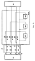
- the second figure shows another embodiment of the invention for a three-phase supply network.
- the third figure shows another embodiment of the invention, also for a three-phase supply network.
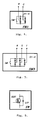
- the 4th figure shows an example of a single-phase switching matrix.
- the 5th figure shows an example of a three-phase switching matrix.
- the 6th figure shows an example of a switching element that was realized with a bipolar transistor insulated base (IGBT) and a diode connected in parallel to it.
- IGBT bipolar transistor insulated base
- the 7th, 8th and 9th figures show current and voltage profiles which characterize the functioning of a circuit arrangement according to the invention.
- the terminals 0, P1 of a single-phase power source are connected to the input terminals P2, P4 of the electronic voltage and / or current compensator ELDC via the supply network ZL.
- the resulting impedance of the supply network ZL is composed of the inductors L0, L1 and resistors R0, R1 of the same network ZL.
- the output terminals P3, P5 of the compensator ELDC are connected to the Leads of load impedance LD connected.
- the primary winding PR of the transformer TR in the compensator ELDC is connected between the input terminal P2 and the output terminal P3 of the same compensator ELDC, the secondary winding SR of the same transformer TR directly or via the filter circuit F and further via the single-phase switching matrix SM1 to the input terminal P4 of the compensator ELDC connected.
- the circuit arrangement according to Figure 1. can be operated in the manner described below:
- the consumer that is drawn with the impedance LD is supplied by the single-phase power source PS. Since a voltage drop occurs at the resulting impedance of the supply network ZL, the voltage present decreases from the output voltage V1 of the current source PS to the input terminals P2, P4 of the compensator ELDC to the voltage value V2.
- the basic function of the switching matrix SM1 corresponds to an idealized switch. According to the invention, the switching matrix SM1 is switched on and off at a frequency that is increased, for example 50 to 100 times higher than the fundamental wave of the current source PS.
- the temporal ratio of the switched on or switched off states and thus the relative pulse width PW is determined by an electronic control part belonging to the circuit arrangement corresponding to the desired output voltage V3.
- the inductance of the primary winding PR of the transformer TR is connected in series with the inductances L0, L1 of the supply network, so that the output voltage V3 becomes lower than the input voltage V2. This means that the voltage can not only be increased but also reduced with this circuit arrangement, which is of particular practical importance.
- the relative pulse width PW can be changed and the voltage V3 that appears at the consumer can be set exactly to a predetermined value. Since the switching frequency of the single-phase switching matrix SM1 is about two orders of magnitude higher than the frequency of the current source PS, in other words, since the single-phase switching matrix SM1 is switched 50 to 100 times within one period of the voltage of the current source PS, it can be achieved be that the voltage V3 not only has the desired mean or effective value, but also follows a predetermined command variable within each period, for example has sinusoidal waveform.
- the voltage induced in the primary winding PR of the transformer TR also has a high-frequency component which suppresses the switching frequency Need to become.
- This type of screening can be carried out either on the primary or on the secondary (possibly simultaneously on both) side (s).
- the screening is carried out with a filter circuit F connected in series with the secondary winding SR on the secondary side.
- the screening on the secondary side has the advantage that the transformer does not have to transmit a high-frequency component, so it can simply be designed for the fundamental waves of current and voltage.
- the required type power of the compensator ELDC is proportional to the extent of the desired compensation. Is e.g. only to compensate for voltage drop in the range of + -10%, the required type power of the compensator ELDC is about 10% of the consumer power.
- the supply lines R, S, T, 0 of the three-phase power source PS are via the supply network ZL, the impedance of which is described with the inductors L1, L2, L3, L0 and with the resistors R1, R2, R3, R0 , connected to the compensator ELDC.
- a primary winding of one of the three transformers TR is inserted into a series connection, the secondary windings SR of the transformers TR directly or indirectly via a filter circuit F and also via a single-phase switching matrix SM1 to the one grounded this time neutral line of the supply network ZL are connected.
- This circuit arrangement essentially contains three single-phase circuit arrangements. The functioning of the circuits belonging to the individual phases completely corresponds to the previous description.
- the voltages or the harmonic contents of the individual phases can be compensated for independently of one another, since the circuits belonging to the individual phases do not interact with one another.
- phase voltages can be compensated in the arrangement according to Figure 3 with the help of the three-phase switching matrix SM3, which contains only a single switching element.
- the single-phase switching matrix SM1 is shown in the fourth figure.
- This exemplary embodiment contains a bridge circuit consisting of diodes D1, D2, D3, D4, in the bridging branch of which there is a semiconductor switching element SW.
- the three-phase switching matrix SM3, which is shown in the 5th figure, contains a three-phase bridge circuit consisting of diodes D1, D2, D3, D4, D5, D6, in the bridging branch of which there is a semiconductor switching element SW.
- the 6th figure shows an embodiment of the semiconductor switching element SW, which consists of a bipolar transistor insulated base (IGBT) and a diode D7 connected between its emitter and collector.
- IGBT bipolar transistor insulated base
- the 7th, 8th and 9th figures show current and voltage curves obtained from computer simulation, in which the frequency of the fundamental wave is 400 Hz, the relative pulse width PW is 60% and the consumer power (in the three phases in total) is 60 kVA.
- the current of the single-phase switching matrix SM1 on the 8th figure the voltage difference V3-V2, and on the 9th figure the output voltage V3 is drawn.
- the frequency of the switching operations is 50 times the frequency of the fundamental wave. It can clearly be seen that the waveform of the output voltage V3 is close to the sinusoidal shape and the mean value of the same output voltage V3 corresponds to the desired mean value.
- the problem solution according to the invention results in a simple structure which can be controlled in a simple manner, and thereby enables the voltage of the consumers to be stabilized with its help and, if necessary, the harmonic content of the current to be compensated at the same time.
- the stabilization of the consumer voltage can not only mean the regulation of its mean or effective value, but also the correction of its distortions (deviations from the sinusoidal shape).
Landscapes
- Engineering & Computer Science (AREA)
- Power Engineering (AREA)
- Physics & Mathematics (AREA)
- Electromagnetism (AREA)
- General Physics & Mathematics (AREA)
- Radar, Positioning & Navigation (AREA)
- Automation & Control Theory (AREA)
- Ac-Ac Conversion (AREA)
Applications Claiming Priority (2)
| Application Number | Priority Date | Filing Date | Title |
|---|---|---|---|
| HU170592 | 1992-05-22 | ||
| HU9201705A HU211048B (en) | 1992-05-22 | 1992-05-22 | Connection arrangement to compensate loss of voltage in power supply cables as well as to reduce harmonic component content of current |
Publications (3)
| Publication Number | Publication Date |
|---|---|
| EP0570839A2 true EP0570839A2 (fr) | 1993-11-24 |
| EP0570839A3 EP0570839A3 (fr) | 1994-11-02 |
| EP0570839B1 EP0570839B1 (fr) | 1996-11-20 |
Family
ID=10981918
Family Applications (1)
| Application Number | Title | Priority Date | Filing Date |
|---|---|---|---|
| EP19930107782 Expired - Lifetime EP0570839B1 (fr) | 1992-05-22 | 1993-05-13 | Circuit de compensation de chute de tension sur les lignes d'alimentation et pour la réduction des ondes harmoniques du courant électrique |
Country Status (3)
| Country | Link |
|---|---|
| EP (1) | EP0570839B1 (fr) |
| DE (1) | DE59304513D1 (fr) |
| HU (1) | HU211048B (fr) |
Cited By (8)
| Publication number | Priority date | Publication date | Assignee | Title |
|---|---|---|---|---|
| WO1995005697A1 (fr) * | 1993-08-13 | 1995-02-23 | Peter Nygren | Dispositif destine a compenser la puissance reactive de systemes electriques |
| WO1998004024A1 (fr) * | 1996-07-18 | 1998-01-29 | Sundstrand Corporation | Systeme de transmission d'energie electrique presentant une ligne d'alimentation de dimension reduite et procede de fonctionnement associe |
| WO1999025061A1 (fr) * | 1997-11-11 | 1999-05-20 | Wolfgang Croce | Circuit de transformation, de commutation, de reglage ou de commande d'une puissance electrique |
| RU2393520C1 (ru) * | 2009-06-16 | 2010-06-27 | Государственное образовательное учреждение высшего профессионального образования "Санкт-Петербургский Государственный политехнический университет" (ГОУ "СПбГПУ") | Способ стабилизации выходного сигнала колебательного объекта |
| RU2410815C1 (ru) * | 2010-01-25 | 2011-01-27 | Василий Сергеевич Богачев | Устройство параметрической стабилизации напряжения переменного тока |
| RU2520572C1 (ru) * | 2013-03-19 | 2014-06-27 | Федеральное государственное бюджетное образовательное учреждение высшего профессионального образования "Томский государственный университет систем управления и радиоэлектроники" (ТУСУР) | Источник питания для электротехнологических установок |
| RU2522913C1 (ru) * | 2013-06-04 | 2014-07-20 | Российская Федерация, от имени которой выступает Государственная корпорация по атомной энергии "Росатом" | Устройство для гальванического разделения сигналов |
| IT202300024852A1 (it) * | 2023-11-23 | 2025-05-23 | Energia Europa S P A | Un sistema per l’attenuazione dei disturbi energetici che si verificano in fase di commutazione di un apparato elettronico per la trasformazione delle caratteristiche di tensione e corrente da fornire ad un carico |
Families Citing this family (1)
| Publication number | Priority date | Publication date | Assignee | Title |
|---|---|---|---|---|
| CN104078975B (zh) * | 2014-07-10 | 2016-06-01 | 国家电网公司 | 单变压器变电站谐波状态估计方法 |
Family Cites Families (1)
| Publication number | Priority date | Publication date | Assignee | Title |
|---|---|---|---|---|
| GB2216348B (en) * | 1988-03-29 | 1992-03-25 | Apv Uk | Power supply circuit |
-
1992
- 1992-05-22 HU HU9201705A patent/HU211048B/hu unknown
-
1993
- 1993-05-13 DE DE59304513T patent/DE59304513D1/de not_active Expired - Fee Related
- 1993-05-13 EP EP19930107782 patent/EP0570839B1/fr not_active Expired - Lifetime
Cited By (10)
| Publication number | Priority date | Publication date | Assignee | Title |
|---|---|---|---|---|
| WO1995005697A1 (fr) * | 1993-08-13 | 1995-02-23 | Peter Nygren | Dispositif destine a compenser la puissance reactive de systemes electriques |
| WO1998004024A1 (fr) * | 1996-07-18 | 1998-01-29 | Sundstrand Corporation | Systeme de transmission d'energie electrique presentant une ligne d'alimentation de dimension reduite et procede de fonctionnement associe |
| US5801460A (en) * | 1996-07-18 | 1998-09-01 | Sundstrand Corporation | Electrical power transmitting system with reduced feeder size and method of operation |
| WO1999025061A1 (fr) * | 1997-11-11 | 1999-05-20 | Wolfgang Croce | Circuit de transformation, de commutation, de reglage ou de commande d'une puissance electrique |
| US6300747B1 (en) | 1997-11-11 | 2001-10-09 | Wolfgang Croce | Circuit having reduced losses occurring during transforming switching adjusting or controlling electric power |
| RU2393520C1 (ru) * | 2009-06-16 | 2010-06-27 | Государственное образовательное учреждение высшего профессионального образования "Санкт-Петербургский Государственный политехнический университет" (ГОУ "СПбГПУ") | Способ стабилизации выходного сигнала колебательного объекта |
| RU2410815C1 (ru) * | 2010-01-25 | 2011-01-27 | Василий Сергеевич Богачев | Устройство параметрической стабилизации напряжения переменного тока |
| RU2520572C1 (ru) * | 2013-03-19 | 2014-06-27 | Федеральное государственное бюджетное образовательное учреждение высшего профессионального образования "Томский государственный университет систем управления и радиоэлектроники" (ТУСУР) | Источник питания для электротехнологических установок |
| RU2522913C1 (ru) * | 2013-06-04 | 2014-07-20 | Российская Федерация, от имени которой выступает Государственная корпорация по атомной энергии "Росатом" | Устройство для гальванического разделения сигналов |
| IT202300024852A1 (it) * | 2023-11-23 | 2025-05-23 | Energia Europa S P A | Un sistema per l’attenuazione dei disturbi energetici che si verificano in fase di commutazione di un apparato elettronico per la trasformazione delle caratteristiche di tensione e corrente da fornire ad un carico |
Also Published As
| Publication number | Publication date |
|---|---|
| HU9201705D0 (en) | 1992-08-28 |
| EP0570839A3 (fr) | 1994-11-02 |
| EP0570839B1 (fr) | 1996-11-20 |
| DE59304513D1 (de) | 1997-01-02 |
| HU211048B (en) | 1995-12-28 |
Similar Documents
| Publication | Publication Date | Title |
|---|---|---|
| EP1311058B1 (fr) | Convertisseur de frequence | |
| DE69005647T2 (de) | System zum ableiten elektrischer energie von einer hochspannungs-gleichstrom-übertragungsleitung. | |
| DE3325612C2 (fr) | ||
| DE69032899T2 (de) | Gleichstrom-leistungstransformator | |
| EP0152002B1 (fr) | Déphaseur | |
| EP1759450B1 (fr) | Circuit commutateur polyphase pauvre en oscillations harmoniques | |
| EP2451065B1 (fr) | Onduleur comporter un convertisseur abaisseur | |
| DE19616591A1 (de) | Stromrichtergerät vom Spannungsquellentyp | |
| DE2446635A1 (de) | Wechselrichteranordnung mit zwei dreiphasigen steuerbaren wechselrichtern | |
| DE2652275A1 (de) | Einrichtung ohne prinzipbedingte verluste zur entnahme von praktisch rein sinusfoermigem, netzfrequentem strom aus wechsel- oder drehspannungsnetzen und zur ueberfuehrung der entnommenen elektrischen energie in galvanisch verbundene gleichspannungssysteme oder gleichspannungszwischensysteme | |
| EP1069673B1 (fr) | Filtre réseau | |
| EP0570839B1 (fr) | Circuit de compensation de chute de tension sur les lignes d'alimentation et pour la réduction des ondes harmoniques du courant électrique | |
| EP0852841B1 (fr) | Transformateur oblique de puissance elevee, compatible avec le reseau, pilote par convertisseur de courant et appliquant une tension | |
| DE3700495A1 (de) | Versorgungsvorrichtung fuer einen wellengenerator fuer ein impulsradar | |
| DE2159030A1 (de) | Stromrichteranordnung | |
| EP0026374B1 (fr) | Dispositif pour le transfert d'énergie électrique de grande puissance d'un réseau d'alimentation triphasé à fréquence plus élevée à un réseau de charge monophasé à fréquence plus basse | |
| DE4446864C2 (de) | Abschaltverfahren für einen dreiphasigen Blindleistungssteller mit zwei Thyristorschaltern | |
| DE3035305C2 (de) | Wechselrichterschaltung für einen Dreiphasen-Synchronmotor | |
| EP3118961B1 (fr) | Utilisation d'une energie de distorsion de reseau electrique a l'aide d'un redresseur | |
| EP3786986B1 (fr) | Circuit de réduction d'une part de flux continu dans le noyau magnétique mou d'un transformateur | |
| DE3418065C2 (fr) | ||
| DE691729C (de) | Verfahren und Einrichtung zum Betrieb einer Gleichstromfernleitung | |
| DE69521998T2 (de) | Schaltungsanordnung | |
| DE1513518B2 (de) | Einrichtung zur zwangskommutierung fuer einen selbstgefuehrten stromrichter zur steuerung der drehzahl und drehrichtung eines drehstrommotors | |
| DE2653137C3 (de) | Mehrphasiger Gleichrichter |
Legal Events
| Date | Code | Title | Description |
|---|---|---|---|
| PUAI | Public reference made under article 153(3) epc to a published international application that has entered the european phase |
Free format text: ORIGINAL CODE: 0009012 |
|
| AK | Designated contracting states |
Kind code of ref document: A2 Designated state(s): CH DE FR LI NL |
|
| TCNL | Nl: translation of patent claims filed | ||
| EL | Fr: translation of claims filed | ||
| PUAL | Search report despatched |
Free format text: ORIGINAL CODE: 0009013 |
|
| AK | Designated contracting states |
Kind code of ref document: A3 Designated state(s): CH DE FR LI NL |
|
| 17P | Request for examination filed |
Effective date: 19950103 |
|
| 17Q | First examination report despatched |
Effective date: 19950814 |
|
| GRAG | Despatch of communication of intention to grant |
Free format text: ORIGINAL CODE: EPIDOS AGRA |
|
| GRAH | Despatch of communication of intention to grant a patent |
Free format text: ORIGINAL CODE: EPIDOS IGRA |
|
| GRAH | Despatch of communication of intention to grant a patent |
Free format text: ORIGINAL CODE: EPIDOS IGRA |
|
| GRAA | (expected) grant |
Free format text: ORIGINAL CODE: 0009210 |
|
| AK | Designated contracting states |
Kind code of ref document: B1 Designated state(s): CH DE FR LI NL |
|
| REF | Corresponds to: |
Ref document number: 59304513 Country of ref document: DE Date of ref document: 19970102 |
|
| ET | Fr: translation filed | ||
| REG | Reference to a national code |
Ref country code: CH Ref legal event code: NV Representative=s name: E. BLUM & CO. PATENTANWAELTE |
|
| PLBI | Opposition filed |
Free format text: ORIGINAL CODE: 0009260 |
|
| 26 | Opposition filed |
Opponent name: SIEMENS AG Effective date: 19970507 |
|
| NLR1 | Nl: opposition has been filed with the epo |
Opponent name: SIEMENS AG |
|
| PLBF | Reply of patent proprietor to notice(s) of opposition |
Free format text: ORIGINAL CODE: EPIDOS OBSO |
|
| PLBF | Reply of patent proprietor to notice(s) of opposition |
Free format text: ORIGINAL CODE: EPIDOS OBSO |
|
| PLBF | Reply of patent proprietor to notice(s) of opposition |
Free format text: ORIGINAL CODE: EPIDOS OBSO |
|
| PLBO | Opposition rejected |
Free format text: ORIGINAL CODE: EPIDOS REJO |
|
| PLBN | Opposition rejected |
Free format text: ORIGINAL CODE: 0009273 |
|
| 27O | Opposition rejected |
Effective date: 20001015 |
|
| NLR2 | Nl: decision of opposition | ||
| PGFP | Annual fee paid to national office [announced via postgrant information from national office to epo] |
Ref country code: FR Payment date: 20010518 Year of fee payment: 9 |
|
| PGFP | Annual fee paid to national office [announced via postgrant information from national office to epo] |
Ref country code: CH Payment date: 20010523 Year of fee payment: 9 |
|
| PGFP | Annual fee paid to national office [announced via postgrant information from national office to epo] |
Ref country code: DE Payment date: 20010528 Year of fee payment: 9 |
|
| PGFP | Annual fee paid to national office [announced via postgrant information from national office to epo] |
Ref country code: NL Payment date: 20010531 Year of fee payment: 9 |
|
| PG25 | Lapsed in a contracting state [announced via postgrant information from national office to epo] |
Ref country code: LI Free format text: LAPSE BECAUSE OF NON-PAYMENT OF DUE FEES Effective date: 20020531 Ref country code: CH Free format text: LAPSE BECAUSE OF NON-PAYMENT OF DUE FEES Effective date: 20020531 |
|
| PG25 | Lapsed in a contracting state [announced via postgrant information from national office to epo] |
Ref country code: NL Free format text: LAPSE BECAUSE OF NON-PAYMENT OF DUE FEES Effective date: 20021201 |
|
| PG25 | Lapsed in a contracting state [announced via postgrant information from national office to epo] |
Ref country code: DE Free format text: LAPSE BECAUSE OF NON-PAYMENT OF DUE FEES Effective date: 20021203 |
|
| REG | Reference to a national code |
Ref country code: CH Ref legal event code: PL |
|
| PG25 | Lapsed in a contracting state [announced via postgrant information from national office to epo] |
Ref country code: FR Free format text: LAPSE BECAUSE OF NON-PAYMENT OF DUE FEES Effective date: 20030131 |
|
| NLV4 | Nl: lapsed or anulled due to non-payment of the annual fee |
Effective date: 20021201 |
|
| REG | Reference to a national code |
Ref country code: FR Ref legal event code: ST |