EP0571756A2 - Innerlich verbundene dreidimensionelle Schaltungsstruktur höherer Dichte - Google Patents
Innerlich verbundene dreidimensionelle Schaltungsstruktur höherer Dichte Download PDFInfo
- Publication number
- EP0571756A2 EP0571756A2 EP93106388A EP93106388A EP0571756A2 EP 0571756 A2 EP0571756 A2 EP 0571756A2 EP 93106388 A EP93106388 A EP 93106388A EP 93106388 A EP93106388 A EP 93106388A EP 0571756 A2 EP0571756 A2 EP 0571756A2
- Authority
- EP
- European Patent Office
- Prior art keywords
- signals
- substrates
- electrical
- substrate
- disposed
- Prior art date
- Legal status (The legal status is an assumption and is not a legal conclusion. Google has not performed a legal analysis and makes no representation as to the accuracy of the status listed.)
- Granted
Links
Images


Classifications
-
- B—PERFORMING OPERATIONS; TRANSPORTING
- B23—MACHINE TOOLS; METAL-WORKING NOT OTHERWISE PROVIDED FOR
- B23K—SOLDERING OR UNSOLDERING; WELDING; CLADDING OR PLATING BY SOLDERING OR WELDING; CUTTING BY APPLYING HEAT LOCALLY, e.g. FLAME CUTTING; WORKING BY LASER BEAM
- B23K15/00—Electron-beam welding or cutting
- B23K15/002—Devices involving relative movement between electron beam and workpiece
-
- B—PERFORMING OPERATIONS; TRANSPORTING
- B23—MACHINE TOOLS; METAL-WORKING NOT OTHERWISE PROVIDED FOR
- B23K—SOLDERING OR UNSOLDERING; WELDING; CLADDING OR PLATING BY SOLDERING OR WELDING; CUTTING BY APPLYING HEAT LOCALLY, e.g. FLAME CUTTING; WORKING BY LASER BEAM
- B23K17/00—Use of the energy of nuclear particles in welding or related techniques
-
- B—PERFORMING OPERATIONS; TRANSPORTING
- B23—MACHINE TOOLS; METAL-WORKING NOT OTHERWISE PROVIDED FOR
- B23K—SOLDERING OR UNSOLDERING; WELDING; CLADDING OR PLATING BY SOLDERING OR WELDING; CUTTING BY APPLYING HEAT LOCALLY, e.g. FLAME CUTTING; WORKING BY LASER BEAM
- B23K26/00—Working by laser beam, e.g. welding, cutting or boring
- B23K26/08—Devices involving relative movement between laser beam and workpiece
-
- G—PHYSICS
- G01—MEASURING; TESTING
- G01P—MEASURING LINEAR OR ANGULAR SPEED, ACCELERATION, DECELERATION, OR SHOCK; INDICATING PRESENCE, ABSENCE, OR DIRECTION, OF MOVEMENT
- G01P15/00—Measuring acceleration; Measuring deceleration; Measuring shock, i.e. sudden change of acceleration
- G01P15/02—Measuring acceleration; Measuring deceleration; Measuring shock, i.e. sudden change of acceleration by making use of inertia forces using solid seismic masses
- G01P15/08—Measuring acceleration; Measuring deceleration; Measuring shock, i.e. sudden change of acceleration by making use of inertia forces using solid seismic masses with conversion into electric or magnetic values
- G01P15/09—Measuring acceleration; Measuring deceleration; Measuring shock, i.e. sudden change of acceleration by making use of inertia forces using solid seismic masses with conversion into electric or magnetic values by piezoelectric pick-up
- G01P15/0922—Measuring acceleration; Measuring deceleration; Measuring shock, i.e. sudden change of acceleration by making use of inertia forces using solid seismic masses with conversion into electric or magnetic values by piezoelectric pick-up of the bending or flexing mode type
-
- G—PHYSICS
- G01—MEASURING; TESTING
- G01P—MEASURING LINEAR OR ANGULAR SPEED, ACCELERATION, DECELERATION, OR SHOCK; INDICATING PRESENCE, ABSENCE, OR DIRECTION, OF MOVEMENT
- G01P15/00—Measuring acceleration; Measuring deceleration; Measuring shock, i.e. sudden change of acceleration
- G01P15/18—Measuring acceleration; Measuring deceleration; Measuring shock, i.e. sudden change of acceleration in two or more dimensions
-
- G—PHYSICS
- G02—OPTICS
- G02B—OPTICAL ELEMENTS, SYSTEMS OR APPARATUS
- G02B6/00—Light guides; Structural details of arrangements comprising light guides and other optical elements, e.g. couplings
- G02B6/10—Light guides; Structural details of arrangements comprising light guides and other optical elements, e.g. couplings of the optical waveguide type
- G02B6/12—Light guides; Structural details of arrangements comprising light guides and other optical elements, e.g. couplings of the optical waveguide type of the integrated circuit kind
- G02B6/12002—Three-dimensional structures
-
- G—PHYSICS
- G02—OPTICS
- G02B—OPTICAL ELEMENTS, SYSTEMS OR APPARATUS
- G02B6/00—Light guides; Structural details of arrangements comprising light guides and other optical elements, e.g. couplings
- G02B6/24—Coupling light guides
- G02B6/42—Coupling light guides with opto-electronic elements
- G02B6/4295—Coupling light guides with opto-electronic elements coupling with semiconductor devices activated by light through the light guide, e.g. thyristors, phototransistors
-
- G—PHYSICS
- G02—OPTICS
- G02B—OPTICAL ELEMENTS, SYSTEMS OR APPARATUS
- G02B6/00—Light guides; Structural details of arrangements comprising light guides and other optical elements, e.g. couplings
- G02B6/24—Coupling light guides
- G02B6/42—Coupling light guides with opto-electronic elements
- G02B6/43—Arrangements comprising a plurality of opto-electronic elements and associated optical interconnections
-
- G—PHYSICS
- G03—PHOTOGRAPHY; CINEMATOGRAPHY; ANALOGOUS TECHNIQUES USING WAVES OTHER THAN OPTICAL WAVES; ELECTROGRAPHY; HOLOGRAPHY
- G03C—PHOTOSENSITIVE MATERIALS FOR PHOTOGRAPHIC PURPOSES; PHOTOGRAPHIC PROCESSES, e.g. CINE, X-RAY, COLOUR, STEREO-PHOTOGRAPHIC PROCESSES; AUXILIARY PROCESSES IN PHOTOGRAPHY
- G03C7/00—Multicolour photographic processes or agents therefor; Regeneration of such processing agents; Photosensitive materials for multicolour processes
- G03C7/22—Subtractive cinematographic processes; Materials therefor; Preparing or processing such materials
- G03C7/24—Subtractive cinematographic processes; Materials therefor; Preparing or processing such materials combined with sound-recording
-
- G—PHYSICS
- G03—PHOTOGRAPHY; CINEMATOGRAPHY; ANALOGOUS TECHNIQUES USING WAVES OTHER THAN OPTICAL WAVES; ELECTROGRAPHY; HOLOGRAPHY
- G03F—PHOTOMECHANICAL PRODUCTION OF TEXTURED OR PATTERNED SURFACES, e.g. FOR PRINTING, FOR PROCESSING OF SEMICONDUCTOR DEVICES; MATERIALS THEREFOR; ORIGINALS THEREFOR; APPARATUS SPECIALLY ADAPTED THEREFOR
- G03F7/00—Photomechanical, e.g. photolithographic, production of textured or patterned surfaces, e.g. printing surfaces; Materials therefor, e.g. comprising photoresists; Apparatus specially adapted therefor
- G03F7/70—Microphotolithographic exposure; Apparatus therefor
- G03F7/70691—Handling of masks or workpieces
-
- G—PHYSICS
- G05—CONTROLLING; REGULATING
- G05B—CONTROL OR REGULATING SYSTEMS IN GENERAL; FUNCTIONAL ELEMENTS OF SUCH SYSTEMS; MONITORING OR TESTING ARRANGEMENTS FOR SUCH SYSTEMS OR ELEMENTS
- G05B19/00—Program-control systems
- G05B19/02—Program-control systems electric
- G05B19/18—Numerical control [NC], i.e. automatically operating machines, in particular machine tools, e.g. in a manufacturing environment, so as to execute positioning, movement or co-ordinated operations by means of program data in numerical form
- G05B19/182—Numerical control [NC], i.e. automatically operating machines, in particular machine tools, e.g. in a manufacturing environment, so as to execute positioning, movement or co-ordinated operations by means of program data in numerical form characterised by the machine tool function, e.g. thread cutting, cam making, tool direction control
- G05B19/186—Generation of screw- or gearlike surfaces
-
- G—PHYSICS
- G12—INSTRUMENT DETAILS
- G12B—CONSTRUCTIONAL DETAILS OF INSTRUMENTS, OR COMPARABLE DETAILS OF OTHER APPARATUS, NOT OTHERWISE PROVIDED FOR
- G12B1/00—Sensitive elements capable of producing movement or displacement for purposes not limited to measurement; Associated transmission mechanisms therefor
-
- H—ELECTRICITY
- H10—SEMICONDUCTOR DEVICES; ELECTRIC SOLID-STATE DEVICES NOT OTHERWISE PROVIDED FOR
- H10D—INORGANIC ELECTRIC SEMICONDUCTOR DEVICES
- H10D62/00—Semiconductor bodies, or regions thereof, of devices having potential barriers
- H10D62/10—Shapes, relative sizes or dispositions of the regions of the semiconductor bodies; Shapes of the semiconductor bodies
- H10D62/117—Shapes of semiconductor bodies
-
- H—ELECTRICITY
- H10—SEMICONDUCTOR DEVICES; ELECTRIC SOLID-STATE DEVICES NOT OTHERWISE PROVIDED FOR
- H10P—GENERIC PROCESSES OR APPARATUS FOR THE MANUFACTURE OR TREATMENT OF DEVICES COVERED BY CLASS H10
- H10P72/00—Handling or holding of wafers, substrates or devices during manufacture or treatment thereof
- H10P72/04—Apparatus for manufacture or treatment
-
- H—ELECTRICITY
- H10—SEMICONDUCTOR DEVICES; ELECTRIC SOLID-STATE DEVICES NOT OTHERWISE PROVIDED FOR
- H10P—GENERIC PROCESSES OR APPARATUS FOR THE MANUFACTURE OR TREATMENT OF DEVICES COVERED BY CLASS H10
- H10P72/00—Handling or holding of wafers, substrates or devices during manufacture or treatment thereof
- H10P72/50—Handling or holding of wafers, substrates or devices during manufacture or treatment thereof for positioning, orientation or alignment
-
- H—ELECTRICITY
- H10—SEMICONDUCTOR DEVICES; ELECTRIC SOLID-STATE DEVICES NOT OTHERWISE PROVIDED FOR
- H10W—GENERIC PACKAGES, INTERCONNECTIONS, CONNECTORS OR OTHER CONSTRUCTIONAL DETAILS OF DEVICES COVERED BY CLASS H10
- H10W40/00—Arrangements for thermal protection or thermal control
- H10W40/40—Arrangements for thermal protection or thermal control involving heat exchange by flowing fluids
- H10W40/47—Arrangements for thermal protection or thermal control involving heat exchange by flowing fluids by flowing liquids, e.g. forced water cooling
-
- H—ELECTRICITY
- H10—SEMICONDUCTOR DEVICES; ELECTRIC SOLID-STATE DEVICES NOT OTHERWISE PROVIDED FOR
- H10W—GENERIC PACKAGES, INTERCONNECTIONS, CONNECTORS OR OTHER CONSTRUCTIONAL DETAILS OF DEVICES COVERED BY CLASS H10
- H10W44/00—Electrical arrangements for controlling or matching impedance
- H10W44/601—Capacitive arrangements
-
- H—ELECTRICITY
- H10—SEMICONDUCTOR DEVICES; ELECTRIC SOLID-STATE DEVICES NOT OTHERWISE PROVIDED FOR
- H10W—GENERIC PACKAGES, INTERCONNECTIONS, CONNECTORS OR OTHER CONSTRUCTIONAL DETAILS OF DEVICES COVERED BY CLASS H10
- H10W70/00—Package substrates; Interposers; Redistribution layers [RDL]
- H10W70/01—Manufacture or treatment
- H10W70/05—Manufacture or treatment of insulating or insulated package substrates, or of interposers, or of redistribution layers
-
- H—ELECTRICITY
- H10—SEMICONDUCTOR DEVICES; ELECTRIC SOLID-STATE DEVICES NOT OTHERWISE PROVIDED FOR
- H10W—GENERIC PACKAGES, INTERCONNECTIONS, CONNECTORS OR OTHER CONSTRUCTIONAL DETAILS OF DEVICES COVERED BY CLASS H10
- H10W70/00—Package substrates; Interposers; Redistribution layers [RDL]
- H10W70/60—Insulating or insulated package substrates; Interposers; Redistribution layers
- H10W70/611—Insulating or insulated package substrates; Interposers; Redistribution layers for connecting multiple chips together
-
- H—ELECTRICITY
- H10—SEMICONDUCTOR DEVICES; ELECTRIC SOLID-STATE DEVICES NOT OTHERWISE PROVIDED FOR
- H10W—GENERIC PACKAGES, INTERCONNECTIONS, CONNECTORS OR OTHER CONSTRUCTIONAL DETAILS OF DEVICES COVERED BY CLASS H10
- H10W70/00—Package substrates; Interposers; Redistribution layers [RDL]
- H10W70/60—Insulating or insulated package substrates; Interposers; Redistribution layers
- H10W70/67—Insulating or insulated package substrates; Interposers; Redistribution layers characterised by their insulating layers or insulating parts
- H10W70/68—Shapes or dispositions thereof
-
- H—ELECTRICITY
- H10—SEMICONDUCTOR DEVICES; ELECTRIC SOLID-STATE DEVICES NOT OTHERWISE PROVIDED FOR
- H10W—GENERIC PACKAGES, INTERCONNECTIONS, CONNECTORS OR OTHER CONSTRUCTIONAL DETAILS OF DEVICES COVERED BY CLASS H10
- H10W90/00—Package configurations
-
- H—ELECTRICITY
- H10—SEMICONDUCTOR DEVICES; ELECTRIC SOLID-STATE DEVICES NOT OTHERWISE PROVIDED FOR
- H10W—GENERIC PACKAGES, INTERCONNECTIONS, CONNECTORS OR OTHER CONSTRUCTIONAL DETAILS OF DEVICES COVERED BY CLASS H10
- H10W90/00—Package configurations
- H10W90/401—Package configurations characterised by multiple insulating or insulated package substrates, interposers or RDLs
-
- H—ELECTRICITY
- H10—SEMICONDUCTOR DEVICES; ELECTRIC SOLID-STATE DEVICES NOT OTHERWISE PROVIDED FOR
- H10W—GENERIC PACKAGES, INTERCONNECTIONS, CONNECTORS OR OTHER CONSTRUCTIONAL DETAILS OF DEVICES COVERED BY CLASS H10
- H10W70/00—Package substrates; Interposers; Redistribution layers [RDL]
- H10W70/60—Insulating or insulated package substrates; Interposers; Redistribution layers
-
- H—ELECTRICITY
- H10—SEMICONDUCTOR DEVICES; ELECTRIC SOLID-STATE DEVICES NOT OTHERWISE PROVIDED FOR
- H10W—GENERIC PACKAGES, INTERCONNECTIONS, CONNECTORS OR OTHER CONSTRUCTIONAL DETAILS OF DEVICES COVERED BY CLASS H10
- H10W72/00—Interconnections or connectors in packages
- H10W72/801—Interconnections on sidewalls of containers
-
- H—ELECTRICITY
- H10—SEMICONDUCTOR DEVICES; ELECTRIC SOLID-STATE DEVICES NOT OTHERWISE PROVIDED FOR
- H10W—GENERIC PACKAGES, INTERCONNECTIONS, CONNECTORS OR OTHER CONSTRUCTIONAL DETAILS OF DEVICES COVERED BY CLASS H10
- H10W90/00—Package configurations
- H10W90/20—Configurations of stacked chips
-
- H—ELECTRICITY
- H10—SEMICONDUCTOR DEVICES; ELECTRIC SOLID-STATE DEVICES NOT OTHERWISE PROVIDED FOR
- H10W—GENERIC PACKAGES, INTERCONNECTIONS, CONNECTORS OR OTHER CONSTRUCTIONAL DETAILS OF DEVICES COVERED BY CLASS H10
- H10W90/00—Package configurations
- H10W90/20—Configurations of stacked chips
- H10W90/291—Configurations of stacked chips characterised by containers, encapsulations, or other housings for the stacked chips
Definitions
- This invention relates to a system for constructing integrated circuits on a plurality of three-dimensional objects and for arranging the objects so that the circuits may be selectively intercoupled, all in a high density configuration.
- circuit boards or chips may be formed in various ways including the use of lithographic techniques which allows for the precise manufacturing and formation of very small details on the circuit board or chip.
- lithographic techniques have in the past generally been limited to the formation of the circuit structures on planar surfaces such as found on boards and chips.
- circuit structures can be provided in which electrical components may be positioned about an entire three-dimensional substrate to both allow for increased density of components for a certain volume and allow for greater exposure of the components for purposes of connecting those components with components on other substrates.
- a three-dimensional electrical circuit structure which includes a plurality of elongate body substrates, each of which includes one or more electrical components disposed on the surface thereof, and electrical conductors also disposed on the surface and coupled to one or more of the electrical components of that substrate.
- the electrical conductors on the elongate body substrates are patterned so that when the substrates are placed in contact with one another, such as side-by-side and in parallel, electrical conductors on each substrate make electrical contact with electrical conductors of at least one other substrate to allow the transfer of electrical signals therebetween.
- the electrical conductors may be disposed at the ends of the substrates, and the substrates formed, so that the substrates may be placed end to end, with the electrical conductors on adjacent substrates making contact to allow exchange of electrical signals between substrates.
- channels for carrying cooling fluid are formed in the elongate body substrates in parallel with the long axes thereof, or between the elongate body substrates when the substrates are positioned or bundled in a contacting, side-by-side, parallel configuration.
- the elongate body substrates may have a variety of cross sections such as circular, oval, triangular, rectangular, hexagonal, etc. as may be desired to carry the circuitry and to allow for electrical conductors on one substrate to contact selected electrical conductors of other substrates when the substrates are bundled or positioned together.
- a building block approach to constructing circuits may be taken in which substrates may be easily added to or taken from the composite whole, for example, to add or subtract memory, add or subtract computational power, etc. This could be done by adding additional substrates to a bundle, removing substrates and replacing them with other substrates, etc. where electrical interconnection to the added substrates is made by contact of surface location conductors. Also, selected interconnections between substrates may be had by proper positioning of the substrates in the bundle, relative to one another, such as by rotating a substrate and/or moving it longitudinally relative to the other substrates.
- FIG. 1 there is shown one illustrative embodiment of a three-dimensional, intercoupled circuit structure made in accordance with the present invention.
- This structure includes a plurality of cylinders 4 made, for example, of an insulator material such as quartz, silica, sapphire, etc., some of said cylinders including axially disposed bores or hollows 6.
- various integrated circuit components 8 fabricated, for example, using non-planar, exposure beam lithography as described in the afore-cited co-pending patent application.
- Such lithography allows for the formation on the surface of three-dimensional objects and bodies of various integrated circuits which otherwise are conventionally formed on planar plates, chips or boards.
- integrated circuit components are not a part of the present invention, and such components could be both active and passive electrical components such as, in the former case, transistors, diodes, semiconductors, etc. and, in the latter case, resistors, capacitors, inductors, etc. These components, in turn, could be fabricated into circuits such as amplifiers, power supplies, modulators and demodulators, etc.
- the circuit components 8 are coupled to electrical conductors or leads 12 formed to extend both longitudinally on the surface of the cylinders and circumferentially thereabout, as shown.
- the conductors on each cylinder 4 are formed and positioned so as to selectively make electrical contact with conductors on adjacent cylinders with which said each cylinder is in contact.
- longitudinal conductors may be coupled to circuit components 8 to extend a distance longitudinally from the component so as to contact a ring or circumferential conductor on an adjacent cylinder when the two cylinders are placed together side-by-side.
- the longitudinal conductors may simply be positioned to connect with ring conductors which circumscribe the cylinder, which ring conductors, in turn, selectively contact ring conductors of adjacent cylinders.
- electrical signals may be transferred not only between circuit components 8 on the same cylinder, but also between circuit components located on different cylinders.
- the cylinders 4 and conductors 12 could be arranged to allow for transferring electrical signals from circuit components 8 on a certain cylinder, via conductors of an adjacent cylinder to circuit components located on a non-adjacent cylinder.
- cooling fluid may be necessary to provide for cooling the circuit components and this is achievable by either directing cooling fluid through the gaps formed between the cylinders when the cylinders are stacked together, or through the hollows 6 formed in the cylinders.
- Such cooling fluid would be applied to an end, intake manifold (not shown), through either the gaps or hollows 6 to an end, outlet manifold 20.
- the use of such cooling fluid would be to maintain an appropriate temperature for the circuit structure and package to ensure proper and reliable operation.
- FIGS. 2A and 2B respectively show a side, elevational view and an end view of a plurality of cylindrical substrates 24 on two of which are formed helical conductors 28, some of which are connected to circuit components 32, and on one of which are formed ring or circumferential conductors 36.
- the helical conductors 28 on the two cylinders 24 are positioned so as to make contact between cylinders and allow for the transfer of electrical signals from components 32 of one cylinder to components 32 on the other cylinder.
- the dots between the cylinders is also illustrated in FIG. 2B, by the dots between the cylinders.
- the ring conductors 36 are formed so as to make contact with at least some of the helical conductors 28 on the adjacent cylinder.
- additional circuitry can be added to and built upon (or removed from) the existing bundle of cylinders and circuits by placing appropriate additional cylinders with circuitry into contact with the existing bundle. For example, if additional memory were to be added to a bundle of cylinders, then a cylinder with such additional memory would be placed into contact with the appropriate existing cylinders in the bundle.
- FIGS. 1, 2A and 2B The disposition of conductors on the cylindrical substrates in FIGS. 1, 2A and 2B is for illustrating that a variety of conductor formations could be provided to allow both for interconnecting circuit components on the same cylindrical substrate and circuit components on different cylindrical substrates.
- FIGS. 3-6 show perspective views of elongate substrates having alternative cross-sections to allow for alternative ways for stacking of the substrates. No circuit components or conductors are shown on the elongate substrates of FIGS. 3-6 but they would be so formed in the same manner as is done for the cylindrical substrates of FIGS. 1 and 2, in accordance with the method of the afore-cited co-pending patent application.
- FIG. 3 shows elongate substrates having triangular cross-sections and centrally disposed bores 40 extending the length of the substrates for carrying a cooling fluid.
- each of the substrates includes flats (side walls) 44 at least some of which on each substrate make contact with the flats of other substrates.
- FIG. 4 is a perspective view of four elongate substrates 48 having centrally disposed bores 52 extending the length thereof for carrying a cooling fluid.
- the substrates 48 may stack or nest together with the flat side walls making intimate contact with the side walls of adjacent substrates.
- FIG. 5 shows elongate substrates 56 having rectangular (square) cross-sections, again with centrally disposed bores or hollows 60 extending the lengths thereof.
- FIG. 6 shows elongate substrate 64 having octagonal cross-sections, also with centrally disposed bores 68 and further with a gap or opening located centrally of the four substrates 64, which could also be utilized for carrying a cooling fluid.
- substrate shapes could be provided so as to allow stacking together of the substrates for the high density packing of circuit components with the capability of electrical signal interchange between substrates.
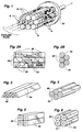
- FIG. 7A is a perspective view showing four cylindrical substrates 76 held together in a nested relationship by a lattice of rods 80.
- the rods 80 advantageously are made of an electrically conductive material to also serve to make contact with conductors 84 on the cylinders 76 to carry electrical signals and provide connections between the cylinders.
- the rods are formed of one set 80a of spaced-apart, generally parallel rods disposed in a plane, and another set 80b of spaced-apart, generally parallel rods disposed in a plane adjacent to and substantially parallel with the first plane so that the one set 80a intersects the other 80b at an acute or right angle to define quadrangular openings 88 in the lattice, each for receiving and holding a different one of the cylinders 76.
- the rods 80 are laterally resilient so as to flex to accommodate receiving and holding of the cylinders and accommodate electrical contact with conductors 84 on the cylinders.
- more than one lattice could be utilized to better hold and support the cylinders; for example, such a lattice could be provided at the end of the cylinders 76 opposite that at which the lattice rods 80 are located.
- FIG. 7B shows an end view of an alternative arrangement for holding cylinder substrates with a lattice.
- three parallel sets of rods 91 are utilized to form triangular openings 92 to hold the cylinders.
- the lattice rods 91 as with the FIG. 7A arrangement, would provide both support and electrical interconnection between the cylinders 92.
- FIG. 8 shows a side, partially cross-sectional view of a generally cylindrical substrate 94 removably disposed in a hollow 96 of a cylindrical substrate 100.
- Circuit components are disposed on the substrate 94, on the exterior thereof to include a pair of sensors 104 suitable, for example, for sensing chemical species (in a chemical composition to which the sensors are exposed), heat, light, electrical fields, etc.
- sensors 104 suitable, for example, for sensing chemical species (in a chemical composition to which the sensors are exposed), heat, light, electrical fields, etc.
- the specific construction of such sensors 104 is not the subject of the present invention but rather, the manner of positioning of sensors on an elongate substrate which may be removably inserted into the hollow of a second substrate to allow for the exchange of electrical signals therebetween.
- the sensors 104 are coupled to a processing circuit 108 which, for example, could process signals received from the sensors 104 to amplify them, reshape them, etc. for transfer onto conductors 112, also formed on the substrate 92.
- the conductors 112, in turn, are coupled to ring conductors 116 which circumscribe the end of the substrate 94 opposite the end at which the sensors 104 are located.
- the ring conductors 116 make contact with a second set of ring conductors 120 which are formed on the inside wall of the hollow 96 to circumscribe the hollow.
- These ring conductors 120 in turn, are coupled to conductors 124 which extend through the hollow to a utilization circuit (not shown) such as, for example, a display means for displaying a value representing the parameter sensed by the sensors 104.
- various sensor substrates could be provided so that if a particular physical parameter were to be sensed, an appropriate sensor substrate could be plugged into the end of substrate 100 so that ring conductors 116 made contact with ring conductors 120, and the sensing operation could then proceed.
- the appropriate sensing substrate 92 for that physical parameter could be selected and plugged into the substrate 100 as earlier described.
- the substrates 94 and 100 are shown to be fairly large in FIG. 8, with the use of the non-planar lithography described in the previously cited co-pending patent application, very small fine-detailed circuit components could be formed on very small substrates of, for example, down to one hundred microns in diameter.
- FIG. 9 shows a pair of cylindrical substrates 130 and 132 spaced apart but positioned generally parallel with one another.
- electrical circuitry is formed on the exterior surface of each of the substrates to include in this instance elements for allowing signalling between the substrates via light, capacitive coupling, or radio frequency signals.
- element 136 on substrate 132 would illustratively be a light emitter such as a photodiode and element 140 on substrate 130 would be a light receiver such as a photocell.
- the light emitting element 136 would energized to produce a light signal which would be received by light receiving element 140 which would produce a signal representing the light signal received, for transfer to a circuit component 144, for example.
- the element 136 on the substrate 132 could simply be a capacitor plate, as would element 140 on substrate 130. Then, when electrical charges were supplied to the element 136, to produce an electrical field directed to element 140, element 140 would produce corresponding charges and thus signals representing the intensity of the electrical field. This information, again, would be passed to circuit component 144 for further processing, for example.
- a dielectric medium represented by arrows 146, could be provided between the plates 136 and 140 and then the dielectric constant varied so as to vary the strength of the electric field detected by plate 140. Varying the dielectric constant could be carried out by simply changing the composition of the dielectric medium as it was passed between the plates 136 and 140.
- element 136 For radio frequency signalling between the substrates 130 and 132, element 136 would be formed to be a transmitting antenna and element 140 would be formed to be a receiving antenna, and then the circuitry on substrate 132 would be formed to include radio frequency signal transmitting circuitry, and the circuitry on substrate 130 would be formed to include radio frequency signal receiving circuitry.
- additional substrates formed in an array with the two substrates 130 and 132 could also be provided to allow for communicating among a large number of substrates.
- the cylinder substrates 130 and 132 of FIG. 9 could be formed of fiber optic strands made, for example, of quartz, silica, sapphire, etc.
- Light represented by arrows 148, could be supplied to and transmitted along the fiber optic strands 130 and 132, and the strands could have formed thereon light detecting elements, such as photocells, for picking up or detecting the intensity of light being transmitted along the strand. Signals representing this detected intensity could be provided to other circuitry formed on the strands, and processed as desired.
- signalling between the substrates can be effected in a variety of ways even without the substrates being in contact with one another, and also that signals can be transmitted along, i.e., inside of, the substrates via the use of light.
- FIG. 10 is a side, elevational view of a pair of cylindrical substrates 154 and 158, one of which (substrate 154) is adapted for sensing a physical parameter, and the other of which (substrate 158) is adapted for emitting a signal identifying the value of the parameter sensed by the first substrate.
- Circuitry is formed on both substrates in a manner already described for carrying out the respective functions of the substrates. Communication between substrate 154 and substrate 158 may be had by an electromagnetic signal transmission such as light or a radio frequency signal.
- the sensor circuitry on substrate 154 might illustratively include circuitry for sensing various chemical species such as described in U. S. Patent No. BI 4,020,830, circuitry for sensing the intensity of light such as by a photocell, circuitry for sensing the temperature of a fluid to which the substrate 154 is exposed, etc.
- Signals produced by the sensing circuitry representing the value of the physical parameter sensed would be processed by other circuitry on the substrate 154 and then signals, again representing the value of the physical parameter sensed, transmitted by the substrate 154 to the substrate 158 as previously mentioned.
- Circuitry on substrate 158 would receive these transmitted signals, and, in turn, produce or cause production of signals for emission outwardly of the substrate, such as light signals or radio frequency signals, indicating the value of the physical parameter sensed.
- FIG. 10 embodiment of the present invention simply shows how a transducer might be constructed for detecting or sensing physical parameters and then emitting a signal representing the value of the sensed parameter.
- communication between the substrate 154 and 158 could be had simply by coupling the two substrates together by an electrical conductor, in lieu of the non-contact communication earlier described.
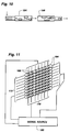
- FIGS. 11 and 12 are perspective views of arrays of substrates suitable for producing optical displays.
- FIG. 11 shows a plurality of cylindrical substrates 164 arranged in parallel in a stack to present a generally planar front surface. Formed on the front surfaces of the substrates 164 are light emitting elements 168, such as light-emitting diodes or the like. Disposed on the back side of the substrates 164 (not seen in FIG. 11) are a plurality of element driving circuits, each coupled to a respective one of the elements 168 and to one horizontal conductor of the conductors 172 and one vertical conductor of the conductors 176. Thus, there are a total of seven (columns) x nine (row) light emitting elements, and the same number of driving circuits coupled to respective light emitting elements.
- Optical displays are produced by supplying electrical signals (from a signal source 180) to selected ones of the horizontal conductors 172 and vertical conductors 176 such that each circuit on the back of the substrates 164 which is connected to a horizontal conductor and vertical conductor which both receive an electrical signal will energize a respective light emitting element 168.
- the circuits on the back of the substrate could utilize simple AND gate logic to determine when both horizontal and vertical conductors to which they were connected receive electrical signals. In this fashion, various optical patterns can be produced on the optical display structure of FIG. 11.
- the FIG. 11 structure could also be adapted to allow for optical detection of light patterns by providing light detecting elements, such as photocells, in place of the light emitting elements 168. Then, when the front surface of the stack of substrates 164 were exposed to a particular light pattern, certain ones of the photocells on the front surfaces of the substrates would detect light, or at least certain levels of light, while others would not and the circuitry on the back of the substrates 164 would produce signals on both the horizontal conductor and vertical conductor to which they are connected. These signals would be supplied to a utilization circuit (in place of signal source 180) connected to both the horizontal conductors 172 and vertical conductors 176 which would determine which photocells detected light and thus determine the light pattern to which the substrate stack was exposed.
- the utilization device 180 for processing the signals on the horizontal conductors 172 and vertical conductors 176 for thus determining the detected light pattern could simply be a microprocessor or other data processing system.
- FIG. 12 is a perspective view of another embodiment of an array of substrates for producing an optical display including a plurality of transparent tubes, made of glass or clear plastic, positioned generally side-by-side and in parallel as shown.
- Each tube 184 is filled with an excitable inert gas such as neon (the tubes 184 would be closed on the ends to prevent the escape of the inert gas, although they are shown as being open in FIG. 12, for illustrative purposes only.
- Threaded through each of the tubes 184 is a different one of a plurality of horizontal electrical conductors 188.
- Disposed on a back side of each of the tubes 184 are elongate conductor strips 192. Extending vertically in parallel with one another to contact each of the conductive strips 192 at different spaced-apart locations along the strips, are a plurality of vertical electrical conductors 196.
- the inert gas located in the general area of the intersection of a horizontal conductor and vertical conductor to which electrical signals are applied will be excited to emit light. Excited areas of gas in the tubes 184 are illustrated by the patches 200 in FIG. 12.
- the electrical signals supplied to only one conductor is insufficient to excite the gas but the electrical signals supplied to two intersecting conductors is sufficient.
- the gas is excited by the electric fields produced by the flow of current through the conductors, which fields, when they exceed a certain level, excite or energize the inert gas in close proximity to such fields.
Landscapes
- Physics & Mathematics (AREA)
- General Physics & Mathematics (AREA)
- Engineering & Computer Science (AREA)
- Optics & Photonics (AREA)
- Mechanical Engineering (AREA)
- High Energy & Nuclear Physics (AREA)
- Automation & Control Theory (AREA)
- Microelectronics & Electronic Packaging (AREA)
- Plasma & Fusion (AREA)
- Human Computer Interaction (AREA)
- Manufacturing & Machinery (AREA)
- Cooling Or The Like Of Electrical Apparatus (AREA)
- Multi-Conductor Connections (AREA)
- Coupling Device And Connection With Printed Circuit (AREA)
- Production Of Multi-Layered Print Wiring Board (AREA)
- Metal Rolling (AREA)
- Diaphragms For Electromechanical Transducers (AREA)
- Combinations Of Printed Boards (AREA)
- Structure Of Printed Boards (AREA)
- Liquid Developers In Electrophotography (AREA)
- Superconductors And Manufacturing Methods Therefor (AREA)
- Cooling Or The Like Of Semiconductors Or Solid State Devices (AREA)
Applications Claiming Priority (2)
| Application Number | Priority Date | Filing Date | Title |
|---|---|---|---|
| US07/871,336 US5270485A (en) | 1991-01-28 | 1992-04-21 | High density, three-dimensional, intercoupled circuit structure |
| US871336 | 1992-04-21 |
Publications (3)
| Publication Number | Publication Date |
|---|---|
| EP0571756A2 true EP0571756A2 (de) | 1993-12-01 |
| EP0571756A3 EP0571756A3 (en) | 1994-06-15 |
| EP0571756B1 EP0571756B1 (de) | 1999-09-15 |
Family
ID=25357225
Family Applications (1)
| Application Number | Title | Priority Date | Filing Date |
|---|---|---|---|
| EP93106388A Expired - Lifetime EP0571756B1 (de) | 1992-04-21 | 1993-04-20 | Innerlich verbundene dreidimensionelle Schaltungsstruktur höherer Dichte |
Country Status (6)
| Country | Link |
|---|---|
| US (1) | US5270485A (de) |
| EP (1) | EP0571756B1 (de) |
| JP (1) | JPH06342991A (de) |
| AT (1) | ATE184730T1 (de) |
| CA (1) | CA2094234C (de) |
| DE (1) | DE69326381T2 (de) |
Families Citing this family (53)
| Publication number | Priority date | Publication date | Assignee | Title |
|---|---|---|---|---|
| US5481184A (en) * | 1991-12-31 | 1996-01-02 | Sarcos Group | Movement actuator/sensor systems |
| US6728113B1 (en) * | 1993-06-24 | 2004-04-27 | Polychip, Inc. | Method and apparatus for non-conductively interconnecting integrated circuits |
| IL106892A0 (en) * | 1993-09-02 | 1993-12-28 | Pierre Badehi | Methods and apparatus for producing integrated circuit devices |
| IL108359A (en) * | 1994-01-17 | 2001-04-30 | Shellcase Ltd | Method and apparatus for producing integrated circuit devices |
| US6898454B2 (en) | 1996-04-25 | 2005-05-24 | The Johns Hopkins University | Systems and methods for evaluating the urethra and the periurethral tissues |
| US6628980B2 (en) | 2000-03-24 | 2003-09-30 | Surgi-Vision, Inc. | Apparatus, systems, and methods for in vivo magnetic resonance imaging |
| US6263229B1 (en) | 1998-11-13 | 2001-07-17 | Johns Hopkins University School Of Medicine | Miniature magnetic resonance catheter coils and related methods |
| US6675033B1 (en) | 1999-04-15 | 2004-01-06 | Johns Hopkins University School Of Medicine | Magnetic resonance imaging guidewire probe |
| US7236816B2 (en) | 1996-04-25 | 2007-06-26 | Johns Hopkins University | Biopsy and sampling needle antennas for magnetic resonance imaging-guided biopsies |
| US6061587A (en) * | 1997-05-15 | 2000-05-09 | Regents Of The University Of Minnesota | Method and apparatus for use with MR imaging |
| US6272370B1 (en) | 1998-08-07 | 2001-08-07 | The Regents Of University Of Minnesota | MR-visible medical device for neurological interventions using nonlinear magnetic stereotaxis and a method imaging |
| US7048716B1 (en) | 1997-05-15 | 2006-05-23 | Stanford University | MR-compatible devices |
| US6026316A (en) * | 1997-05-15 | 2000-02-15 | Regents Of The University Of Minnesota | Method and apparatus for use with MR imaging |
| US5964705A (en) * | 1997-08-22 | 1999-10-12 | Image-Guided Drug Delivery System, Inc. | MR-compatible medical devices |
| DE19750064A1 (de) * | 1997-11-12 | 1999-05-20 | Cit Alcatel | Mehrfachparallelleiter für Wicklungen elektrischer Geräte und Maschinen |
| US6063200A (en) * | 1998-02-10 | 2000-05-16 | Sarcos L.C. | Three-dimensional micro fabrication device for filamentary substrates |
| US6463317B1 (en) | 1998-05-19 | 2002-10-08 | Regents Of The University Of Minnesota | Device and method for the endovascular treatment of aneurysms |
| EP1171032A4 (de) | 1999-04-15 | 2008-10-29 | Surgi Vision | Verfahren für in vivo bildgebung mittels magnetischer resonanz |
| US7848788B2 (en) | 1999-04-15 | 2010-12-07 | The Johns Hopkins University | Magnetic resonance imaging probe |
| DE60143258D1 (de) | 2000-02-01 | 2010-11-25 | Surgivision Inc | Transseptale nadelantenne für ein mr-bildgebungsgerät |
| US6576406B1 (en) | 2000-06-29 | 2003-06-10 | Sarcos Investments Lc | Micro-lithographic method and apparatus using three-dimensional mask |
| JP4401037B2 (ja) | 2001-04-03 | 2010-01-20 | Necエレクトロニクス株式会社 | 半導体装置及びその製造方法 |
| US20030059526A1 (en) * | 2001-09-12 | 2003-03-27 | Benson Martin H. | Apparatus and method for the design and manufacture of patterned multilayer thin films and devices on fibrous or ribbon-like substrates |
| TW560102B (en) * | 2001-09-12 | 2003-11-01 | Itn Energy Systems Inc | Thin-film electrochemical devices on fibrous or ribbon-like substrates and methd for their manufacture and design |
| WO2003022564A1 (en) * | 2001-09-12 | 2003-03-20 | Itn Energy Systems, Inc. | Apparatus and method for the design and manufacture of multifunctional composite materials with power integration |
| US20050156282A1 (en) * | 2004-01-13 | 2005-07-21 | Yoram Palti | Semiconductor device and method of its manufacture |
| US20050180675A1 (en) * | 2004-02-12 | 2005-08-18 | Panorama Flat Limited, A Western Australia Corporation | Apparatus, method, and computer program product for structured waveguide including performance_enhancing bounding region |
| US20060056792A1 (en) * | 2004-02-12 | 2006-03-16 | Panorama Flat Ltd. | System, method, and computer program product for structured waveguide including intra/inter contacting regions |
| US20050180672A1 (en) * | 2004-02-12 | 2005-08-18 | Panorama Flat Ltd. | Apparatus, Method, and Computer Program Product For Multicolor Structured Waveguide |
| US20050180722A1 (en) * | 2004-02-12 | 2005-08-18 | Panorama Flat Ltd. | Apparatus, method, and computer program product for structured waveguide transport |
| US20060056793A1 (en) * | 2004-02-12 | 2006-03-16 | Panorama Flat Ltd. | System, method, and computer program product for structured waveguide including nonlinear effects |
| US7224854B2 (en) * | 2004-02-12 | 2007-05-29 | Panorama Labs Pty. Ltd. | System, method, and computer program product for structured waveguide including polarizer region |
| US20050201705A1 (en) * | 2004-02-12 | 2005-09-15 | Panorama Flat Ltd. | Apparatus, method, and computer program product for structured waveguide including recursion zone |
| US20050185877A1 (en) * | 2004-02-12 | 2005-08-25 | Panorama Flat Ltd. | Apparatus, Method, and Computer Program Product For Structured Waveguide Switching Matrix |
| US20050180723A1 (en) * | 2004-02-12 | 2005-08-18 | Panorama Flat Ltd. | Apparatus, method, and computer program product for structured waveguide including holding bounding region |
| US7254287B2 (en) * | 2004-02-12 | 2007-08-07 | Panorama Labs, Pty Ltd. | Apparatus, method, and computer program product for transverse waveguided display system |
| US20050201679A1 (en) * | 2004-02-12 | 2005-09-15 | Panorama Flat Ltd. | System, method, and computer program product for structured waveguide including modified output regions |
| US20050201654A1 (en) * | 2004-02-12 | 2005-09-15 | Panorama Flat Ltd. | Apparatus, method, and computer program product for substrated waveguided display system |
| US20050180674A1 (en) * | 2004-02-12 | 2005-08-18 | Panorama Flat Ltd. | Faraday structured waveguide display |
| US20060056794A1 (en) * | 2004-02-12 | 2006-03-16 | Panorama Flat Ltd. | System, method, and computer program product for componentized displays using structured waveguides |
| US20050180673A1 (en) * | 2004-02-12 | 2005-08-18 | Panorama Flat Ltd. | Faraday structured waveguide |
| US20050201651A1 (en) * | 2004-02-12 | 2005-09-15 | Panorama Flat Ltd. | Apparatus, method, and computer program product for integrated influencer element |
| US20050201698A1 (en) * | 2004-02-12 | 2005-09-15 | Panorama Flat Ltd. | System, method, and computer program product for faceplate for structured waveguide system |
| US20060074295A1 (en) * | 2004-10-01 | 2006-04-06 | Nexgen | Combined MR coil technology in medical devices |
| US7425760B1 (en) | 2004-10-13 | 2008-09-16 | Sun Microsystems, Inc. | Multi-chip module structure with power delivery using flexible cables |
| US7603153B2 (en) * | 2005-12-12 | 2009-10-13 | Sterling Investments Lc | Multi-element probe array |
| US7333699B2 (en) * | 2005-12-12 | 2008-02-19 | Raytheon Sarcos, Llc | Ultra-high density connector |
| US7999471B2 (en) * | 2005-12-12 | 2011-08-16 | Raytheon Company | Multi-cell electronic circuit array and method of manufacturing |
| US7626123B2 (en) * | 2005-12-12 | 2009-12-01 | Raytheon Sarcos, Llc | Electrical microfilament to circuit interface |
| US20080038704A1 (en) * | 2006-06-29 | 2008-02-14 | Careguide Systems, Inc. | Integrated blood pressure control and coronary artery self-care system and method |
| US20080050709A1 (en) * | 2006-06-29 | 2008-02-28 | Careguide Systems, Inc. | Integrated blood sugar control, blood pressure control and heart failure self-care system and method |
| US20080064016A1 (en) * | 2006-06-29 | 2008-03-13 | Careguide Systems, Inc. | Integrated blood sugar control, blood pressure control and coronary artery self-care system and method |
| US9299686B1 (en) | 2015-01-16 | 2016-03-29 | International Business Machines Corporation | Implementing integrated circuit chip attach in three dimensional stack using vapor deposited solder Cu pillars |
Family Cites Families (18)
| Publication number | Priority date | Publication date | Assignee | Title |
|---|---|---|---|---|
| US3401448A (en) * | 1964-06-22 | 1968-09-17 | Globe Union Inc | Process for making photosensitive semiconductor devices |
| DE1665794C3 (de) * | 1966-10-28 | 1974-06-12 | Siemens Ag, 1000 Berlin Und 8000 Muenchen | Verfahren zum Herstellen einer magnetfeldabhängigen Widerstandsanordnung |
| US3875479A (en) * | 1973-05-07 | 1975-04-01 | Gilbert R Jaggar | Electrical apparatus |
| US3976508A (en) * | 1974-11-01 | 1976-08-24 | Mobil Tyco Solar Energy Corporation | Tubular solar cell devices |
| US4020830A (en) * | 1975-03-12 | 1977-05-03 | The University Of Utah | Selective chemical sensitive FET transducers |
| DE2848502A1 (de) * | 1978-11-08 | 1980-07-17 | Max Planck Gesellschaft | Kuehlvorrichtung fuer elektronische geraete und verfahren zu ihrer herstellung |
| CH665908A5 (de) * | 1983-08-30 | 1988-06-15 | Cerberus Ag | Vorrichtung zum selektiven detektieren der gasfoermigen bestandteile von gasgemischen in luft mittels eines gassensors. |
| US4542640A (en) * | 1983-09-15 | 1985-09-24 | Clifford Paul K | Selective gas detection and measurement system |
| US4617160A (en) * | 1984-11-23 | 1986-10-14 | Irvine Sensors Corporation | Method for fabricating modules comprising uniformly stacked, aligned circuit-carrying layers |
| JPS61168951A (ja) * | 1985-01-22 | 1986-07-30 | Nippon Telegr & Teleph Corp <Ntt> | 半導体集積回路チツプの実装構造 |
| US5016138A (en) * | 1987-10-27 | 1991-05-14 | Woodman John K | Three dimensional integrated circuit package |
| US4858072A (en) * | 1987-11-06 | 1989-08-15 | Ford Aerospace & Communications Corporation | Interconnection system for integrated circuit chips |
| CA1283225C (en) * | 1987-11-09 | 1991-04-16 | Shinji Mine | Cooling system for three-dimensional ic package |
| JPH03185900A (ja) * | 1989-12-15 | 1991-08-13 | Hitachi Ltd | 半導体装置及びその製造方法 |
| JP2995076B2 (ja) * | 1990-07-24 | 1999-12-27 | 富士通株式会社 | 半導体装置 |
| US5124508A (en) * | 1990-08-14 | 1992-06-23 | The Scabbard Corp. | Application of sheet batteries as support base for electronic circuits |
| US5053856A (en) * | 1990-09-04 | 1991-10-01 | Sun Microsystems, Inc. | Apparatus for providing electrical conduits in compact arrays of electronic circuitry utilizing cooling devices |
| US5106455A (en) * | 1991-01-28 | 1992-04-21 | Sarcos Group | Method and apparatus for fabrication of micro-structures using non-planar, exposure beam lithography |
-
1992
- 1992-04-21 US US07/871,336 patent/US5270485A/en not_active Expired - Lifetime
-
1993
- 1993-04-16 CA CA002094234A patent/CA2094234C/en not_active Expired - Lifetime
- 1993-04-20 EP EP93106388A patent/EP0571756B1/de not_active Expired - Lifetime
- 1993-04-20 JP JP5093167A patent/JPH06342991A/ja active Pending
- 1993-04-20 AT AT93106388T patent/ATE184730T1/de not_active IP Right Cessation
- 1993-04-20 DE DE69326381T patent/DE69326381T2/de not_active Expired - Lifetime
Also Published As
| Publication number | Publication date |
|---|---|
| DE69326381T2 (de) | 2000-02-24 |
| JPH06342991A (ja) | 1994-12-13 |
| CA2094234A1 (en) | 1993-10-22 |
| EP0571756A3 (en) | 1994-06-15 |
| CA2094234C (en) | 2005-05-31 |
| DE69326381D1 (de) | 1999-10-21 |
| EP0571756B1 (de) | 1999-09-15 |
| ATE184730T1 (de) | 1999-10-15 |
| US5270485A (en) | 1993-12-14 |
Similar Documents
| Publication | Publication Date | Title |
|---|---|---|
| US5634194A (en) | High density, three-dimensional, intercoupled circuit structure | |
| US5270485A (en) | High density, three-dimensional, intercoupled circuit structure | |
| US5673131A (en) | High density, three-dimensional, intercoupled circuit structure | |
| US5785321A (en) | Roulette registration system | |
| US6856715B1 (en) | Apparatus comprising electronic and/or optoelectronic circuitry and method for realizing said circuitry | |
| US7228051B2 (en) | Light pipe with alignment structures | |
| US20140254140A1 (en) | Led backlight system for cabinet sign | |
| FR2507800B1 (fr) | Procede de fabrication d'une carte d'identification comportant un module incorpore a circuit integre | |
| US20030142913A1 (en) | Fiber-free optical interconnect system for chip-to-chip signaling | |
| JPH05183679A (ja) | 原稿読み取り装置 | |
| CN107438900B (zh) | 辐射传感器 | |
| US4524240A (en) | Universal circuit prototyping board | |
| EP0369427A3 (de) | Halbleitervorrichtung | |
| FR2667444B1 (fr) | Element a emission de champ et son procede de fabrication. | |
| GB2099221B (en) | Light emitting diode array devices and image transfer systems | |
| US6780672B2 (en) | Micro eletro-mechanical component and system architecture | |
| US3943021A (en) | Optical data processing system | |
| US6356089B2 (en) | Contact probe arrangement | |
| EP0224901A2 (de) | Hoch auflösende, optische Faseranordnung und Objektpositionsbestimmungssystem | |
| FR2742578B1 (fr) | Cathode a emission de champ et son procede de fabrication | |
| US20080107373A1 (en) | Diffusion and Laser Photoelectrically Coupled Integrated Circuit Signal Line | |
| FR2638000B1 (fr) | Carte a memoire magnetique a grande capacite et procede de fabrication | |
| US4879465A (en) | Detector module for scintillation cameras | |
| EP0461579A2 (de) | Lichtemittierende Vorrichtung | |
| US3335265A (en) | Punched card reader |
Legal Events
| Date | Code | Title | Description |
|---|---|---|---|
| PUAI | Public reference made under article 153(3) epc to a published international application that has entered the european phase |
Free format text: ORIGINAL CODE: 0009012 |
|
| AK | Designated contracting states |
Kind code of ref document: A2 Designated state(s): AT BE CH DE DK ES FR GB GR IE IT LI NL PT SE |
|
| PUAL | Search report despatched |
Free format text: ORIGINAL CODE: 0009013 |
|
| AK | Designated contracting states |
Kind code of ref document: A3 Designated state(s): AT BE CH DE DK ES FR GB GR IE IT LI NL PT SE |
|
| 17P | Request for examination filed |
Effective date: 19941209 |
|
| 17Q | First examination report despatched |
Effective date: 19960718 |
|
| GRAG | Despatch of communication of intention to grant |
Free format text: ORIGINAL CODE: EPIDOS AGRA |
|
| GRAG | Despatch of communication of intention to grant |
Free format text: ORIGINAL CODE: EPIDOS AGRA |
|
| GRAH | Despatch of communication of intention to grant a patent |
Free format text: ORIGINAL CODE: EPIDOS IGRA |
|
| GRAH | Despatch of communication of intention to grant a patent |
Free format text: ORIGINAL CODE: EPIDOS IGRA |
|
| GRAA | (expected) grant |
Free format text: ORIGINAL CODE: 0009210 |
|
| AK | Designated contracting states |
Kind code of ref document: B1 Designated state(s): AT BE CH DE DK ES FR GB GR IE IT LI NL PT SE |
|
| PG25 | Lapsed in a contracting state [announced via postgrant information from national office to epo] |
Ref country code: SE Free format text: THE PATENT HAS BEEN ANNULLED BY A DECISION OF A NATIONAL AUTHORITY Effective date: 19990915 Ref country code: NL Free format text: LAPSE BECAUSE OF FAILURE TO SUBMIT A TRANSLATION OF THE DESCRIPTION OR TO PAY THE FEE WITHIN THE PRESCRIBED TIME-LIMIT Effective date: 19990915 Ref country code: IT Free format text: LAPSE BECAUSE OF FAILURE TO SUBMIT A TRANSLATION OF THE DESCRIPTION OR TO PAY THE FEE WITHIN THE PRE;WARNING: LAPSES OF ITALIAN PATENTS WITH EFFECTIVE DATE BEFORE 2007 MAY HAVE OCCURRED AT ANY TIME BEFORE 2007. THE CORRECT EFFECTIVE DATE MAY BE DIFFERENT FROM THE ONE RECORDED.SCRIBED TIME-LIMIT Effective date: 19990915 Ref country code: GR Free format text: LAPSE BECAUSE OF NON-PAYMENT OF DUE FEES Effective date: 19990915 Ref country code: ES Free format text: THE PATENT HAS BEEN ANNULLED BY A DECISION OF A NATIONAL AUTHORITY Effective date: 19990915 Ref country code: AT Free format text: LAPSE BECAUSE OF FAILURE TO SUBMIT A TRANSLATION OF THE DESCRIPTION OR TO PAY THE FEE WITHIN THE PRESCRIBED TIME-LIMIT Effective date: 19990915 |
|
| REF | Corresponds to: |
Ref document number: 184730 Country of ref document: AT Date of ref document: 19991015 Kind code of ref document: T |
|
| REG | Reference to a national code |
Ref country code: CH Ref legal event code: NV Representative=s name: PATENTANWALTSBUERO JEAN HUNZIKER Ref country code: CH Ref legal event code: EP |
|
| REF | Corresponds to: |
Ref document number: 69326381 Country of ref document: DE Date of ref document: 19991021 |
|
| REG | Reference to a national code |
Ref country code: IE Ref legal event code: FG4D |
|
| PG25 | Lapsed in a contracting state [announced via postgrant information from national office to epo] |
Ref country code: PT Free format text: LAPSE BECAUSE OF FAILURE TO SUBMIT A TRANSLATION OF THE DESCRIPTION OR TO PAY THE FEE WITHIN THE PRESCRIBED TIME-LIMIT Effective date: 19991215 Ref country code: DK Free format text: LAPSE BECAUSE OF FAILURE TO SUBMIT A TRANSLATION OF THE DESCRIPTION OR TO PAY THE FEE WITHIN THE PRESCRIBED TIME-LIMIT Effective date: 19991215 |
|
| ET | Fr: translation filed | ||
| NLV1 | Nl: lapsed or annulled due to failure to fulfill the requirements of art. 29p and 29m of the patents act | ||
| PG25 | Lapsed in a contracting state [announced via postgrant information from national office to epo] |
Ref country code: IE Free format text: LAPSE BECAUSE OF NON-PAYMENT OF DUE FEES Effective date: 20000420 |
|
| PLBE | No opposition filed within time limit |
Free format text: ORIGINAL CODE: 0009261 |
|
| 26N | No opposition filed | ||
| REG | Reference to a national code |
Ref country code: IE Ref legal event code: MM4A |
|
| REG | Reference to a national code |
Ref country code: GB Ref legal event code: IF02 |
|
| PGFP | Annual fee paid to national office [announced via postgrant information from national office to epo] |
Ref country code: BE Payment date: 20020429 Year of fee payment: 10 |
|
| PGFP | Annual fee paid to national office [announced via postgrant information from national office to epo] |
Ref country code: CH Payment date: 20020430 Year of fee payment: 10 Ref country code: GB Payment date: 20020430 Year of fee payment: 10 |
|
| PG25 | Lapsed in a contracting state [announced via postgrant information from national office to epo] |
Ref country code: GB Free format text: LAPSE BECAUSE OF NON-PAYMENT OF DUE FEES Effective date: 20030420 |
|
| PG25 | Lapsed in a contracting state [announced via postgrant information from national office to epo] |
Ref country code: LI Free format text: LAPSE BECAUSE OF NON-PAYMENT OF DUE FEES Effective date: 20030430 Ref country code: CH Free format text: LAPSE BECAUSE OF NON-PAYMENT OF DUE FEES Effective date: 20030430 Ref country code: BE Free format text: LAPSE BECAUSE OF NON-PAYMENT OF DUE FEES Effective date: 20030430 |
|
| BERE | Be: lapsed |
Owner name: *SARCOS GROUP Effective date: 20030430 |
|
| GBPC | Gb: european patent ceased through non-payment of renewal fee |
Effective date: 20030420 |
|
| REG | Reference to a national code |
Ref country code: CH Ref legal event code: PL |
|
| PGFP | Annual fee paid to national office [announced via postgrant information from national office to epo] |
Ref country code: FR Payment date: 20110426 Year of fee payment: 19 Ref country code: DE Payment date: 20110413 Year of fee payment: 19 |
|
| REG | Reference to a national code |
Ref country code: FR Ref legal event code: ST Effective date: 20121228 |
|
| REG | Reference to a national code |
Ref country code: DE Ref legal event code: R119 Ref document number: 69326381 Country of ref document: DE Effective date: 20121101 |
|
| PG25 | Lapsed in a contracting state [announced via postgrant information from national office to epo] |
Ref country code: FR Free format text: LAPSE BECAUSE OF NON-PAYMENT OF DUE FEES Effective date: 20120430 |
|
| PG25 | Lapsed in a contracting state [announced via postgrant information from national office to epo] |
Ref country code: DE Free format text: LAPSE BECAUSE OF NON-PAYMENT OF DUE FEES Effective date: 20121101 |