EP0571905A2 - Modulationsverfahren - Google Patents
Modulationsverfahren Download PDFInfo
- Publication number
- EP0571905A2 EP0571905A2 EP93108290A EP93108290A EP0571905A2 EP 0571905 A2 EP0571905 A2 EP 0571905A2 EP 93108290 A EP93108290 A EP 93108290A EP 93108290 A EP93108290 A EP 93108290A EP 0571905 A2 EP0571905 A2 EP 0571905A2
- Authority
- EP
- European Patent Office
- Prior art keywords
- numerical value
- minimum
- error rate
- relationship
- data
- Prior art date
- Legal status (The legal status is an assumption and is not a legal conclusion. Google has not performed a legal analysis and makes no representation as to the accuracy of the status listed.)
- Granted
Links
Images




Classifications
-
- G—PHYSICS
- G11—INFORMATION STORAGE
- G11B—INFORMATION STORAGE BASED ON RELATIVE MOVEMENT BETWEEN RECORD CARRIER AND TRANSDUCER
- G11B20/00—Signal processing not specific to the method of recording or reproducing; Circuits therefor
- G11B20/10—Digital recording or reproducing
-
- G—PHYSICS
- G11—INFORMATION STORAGE
- G11B—INFORMATION STORAGE BASED ON RELATIVE MOVEMENT BETWEEN RECORD CARRIER AND TRANSDUCER
- G11B20/00—Signal processing not specific to the method of recording or reproducing; Circuits therefor
- G11B20/10—Digital recording or reproducing
- G11B20/14—Digital recording or reproducing using self-clocking codes
- G11B20/1403—Digital recording or reproducing using self-clocking codes characterised by the use of two levels
- G11B20/1423—Code representation depending on subsequent bits, e.g. delay modulation, double density code, Miller code
- G11B20/1426—Code representation depending on subsequent bits, e.g. delay modulation, double density code, Miller code conversion to or from block codes or representations thereof
Definitions
- the present invention relates to a modulating method adapted for use in digitally recording data on a recording medium and, more particularly, in determining the optimal range of a minimum run length d (minimum number of successive same symbols) in a variable-length code (d, k; m, n; r).
- a magnetic recording system for example, generally its signal frequency characteristic is differential, and there occurs deterioration of the characteristic in a higher frequency range of the signal. Such deterioration is derived from, e.g., a variety of losses relative to a head gap, the space between a head and a recording medium, the thickness of a recording medium, and low-frequency loss caused by a rotary transformer.
- random errors are induced by crosstalk noise from adjacent tracks, noise from a recording medium, or overwrite noise.
- the digital data is modulated, prior to being recorded on a medium, in a manner to be adequate for the recording system, whereby a greater amount of the information can be recorded with stability.
- it is generally customary to channel-code the data in accordance with predetermined rules.
- the output of the error corrector 36 is supplied via the buffer 37 to the demultiplexer 38 so as to be separated into the video data and the audio data.
- the audio data is supplied to the A-D converter 39 for analog-to-digital conversion, while the video data is supplied to the A-D converter 40 for the same conversion.
- the video signal and the audio signal outputted from the A-D converters 39 and 40 respectively are supplied to an unshown monitor.
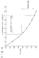
- the S/N needs to be approximately 21dB to 22dB, as will be understood from Fig. 2.
- a routine for deciding the optimal range of the minimum run length d (minimum number of successive same symbols) by the modulating method of the present invention is started at step 51.
- the surface density is increased 3.0 times in the use of a green laser having a wavelength of 532 nm, or 4.2 times in the use of a blue laser having a wavelength of 420 nm.
- NA numerical aperture
- the capacity can be increased 2.8 times in using the red laser, 6.0 times in using the green laser, or 8.4 times in using the blue laser.
- a data word having a 2-bit basic data length is converted to a code word having a 5-bit basic code length.
- Table 4 shows six kinds of basic codes used for such conversion. Digital data can be converted to variable-length code words by combining such six kinds of basic codes. TABLE 4 1 1 0 0 0 0 2 0 1 0 0 0 3 0 0 1 0 0 4 0 0 0 1 0 5 0 0 0 0 1 6 0 0 0 0 0 0 0 0 0 0 0
- Table 5 shows the number of effective codes obtained by the use of such basic codes.
- the code words where the restriction length r is chargeable up to 5 to convert the original data into code words properly without any excess or deficiency.
- Tables 6 and 7 are specific examples for converting the digital data to code words by using the basic codes in Table 4.
- digital data of a 2-bit basic data length is converted to a code word of a 5-bit basic code length.
- data "11” is converted to a code "00000”, and data "10” to a code "10000”.
- data of 4-, 6-, 8- and 10-bit lengths are converted respectively to code words having 10-, 15-, 20- and 25-bit code lengths.
- Fig. 6 is a block diagram showing an exemplary constitution of the modulator 19 employed in the apparatus of Fig. 1.
- Digital data is sequentially inputted to a shift register 61 in synchronism with data clock pulses.
- 10-bit digital data is stored in the shift register 61.
- the data outputted from the shift register 61 is supplied to an encoder 62, where the restriction length r is decided.
- the digital data supplied from the shift register 61 is delivered via the encoder 62 to a selector 63.
- the restriction length r is decided to be 2, and the data is supplied to the ROM 64-2. Then the data is converted to a code "0100000000" in accordance with the table stored therein.
- Fig. 7 shows an example of such conversion.
- the input digital data is 18D2 (Fig. 7(a)) in hexadecimal notation.
- its binary data (Fig. 7(b)) is "0001100011010010”.
- the encoder 2 decides the restriction length r of the input binary data as follows.
- the data corresponding to the first 2 bits "00" is not existent in Table 6. Therefore a decision is made as to whether the 4-bit data "0001" inclusive of the succeeding 2-bit data is existent in Table 6. However, this data is not existent either in Table 6.
- the code words thus converted through the ROMs 64-1 - 64-6 are supplied to the multiplexer 5 and are mutually combined to form a code word of successive bits.
- delimiters of this code word are positioned at the first 20 bits, the next 5 bits, the following 10 bits and the 5 bits posterior thereto (Fig. 7(d)) .
- a multiplexer 84 combines the data read out from the ROMs 83-1 - 83-6 and delivers the composite data to a buffer 85. Subsequently the data read out from the buffer 85 is supplied to a deformatter 86, and the deformatted data therefrom is supplied to an error corrector 86.
- a reference clock generator 87 generates a reference clock signal synchronized with the input code word and supplies the clock signal to both the buffer 85 and a sync detector 88. Then the sync detector 88 detects the sync signal position of the code word on the basis of the reference clock signal supplied thereto from the reference clock generator 87. And the detected signal is supplied to the ROM 83.
- the conversion length detector 81 detects the conversion length of the input code word and controls the selector 82 in conformity with the result of such detection, whereby the code word having a 5-bit basic code length is supplied to the ROM 83-1, while the code word having a 10-bit basic code length is supplied to the ROM 83-2. Similarly, the code words having 15-bit, 20-bit and 25-bit basic code word lengths individually are supplied to the ROMs 83-3 - 83-5 respectively. When the input code word has a 15-bit length as "000010000100000", it is supplied to the ROM 83-6.
- the code words inputted to the ROMs 83-1 - 83-6 are decoded to become the original data in accordance with the tables stored therein respectively.
- the digital data decoded by means of the ROMs 83-1 - 83-6 are combined with one another by the multiplexer 84, and the composite data is written in the buffer 85. Subsequently the data read out from the buffer 85 is supplied to the deformatter 86 and, after the process of separating the sync signal and so forth, the data is supplied to the error corrector 36.
Landscapes
- Signal Processing (AREA)
- Engineering & Computer Science (AREA)
- Signal Processing For Digital Recording And Reproducing (AREA)
- Optical Recording Or Reproduction (AREA)
- Liquid Crystal (AREA)
- Amplifiers (AREA)
- Crystals, And After-Treatments Of Crystals (AREA)
- Ultra Sonic Daignosis Equipment (AREA)
- Magnetic Resonance Imaging Apparatus (AREA)
- Radar Systems Or Details Thereof (AREA)
- Optical Communication System (AREA)
- Compression, Expansion, Code Conversion, And Decoders (AREA)
- Transition And Organic Metals Composition Catalysts For Addition Polymerization (AREA)
- Liquid Crystal Substances (AREA)
- Pharmaceuticals Containing Other Organic And Inorganic Compounds (AREA)
Applications Claiming Priority (2)
| Application Number | Priority Date | Filing Date | Title |
|---|---|---|---|
| JP157558/92 | 1992-05-25 | ||
| JP15755892A JP3427392B2 (ja) | 1992-05-25 | 1992-05-25 | 符号化方法 |
Publications (3)
| Publication Number | Publication Date |
|---|---|
| EP0571905A2 true EP0571905A2 (de) | 1993-12-01 |
| EP0571905A3 EP0571905A3 (de) | 1995-06-07 |
| EP0571905B1 EP0571905B1 (de) | 1998-08-19 |
Family
ID=15652311
Family Applications (1)
| Application Number | Title | Priority Date | Filing Date |
|---|---|---|---|
| EP93108290A Expired - Lifetime EP0571905B1 (de) | 1992-05-25 | 1993-05-21 | Modulationsverfahren |
Country Status (12)
| Country | Link |
|---|---|
| US (1) | US5432799A (de) |
| EP (1) | EP0571905B1 (de) |
| JP (1) | JP3427392B2 (de) |
| KR (1) | KR100263686B1 (de) |
| CN (1) | CN1061159C (de) |
| AT (1) | ATE170019T1 (de) |
| AU (1) | AU656675B2 (de) |
| CA (1) | CA2096792A1 (de) |
| DE (1) | DE69320403T2 (de) |
| ES (1) | ES2119833T3 (de) |
| MY (1) | MY109819A (de) |
| TW (1) | TW342561B (de) |
Cited By (2)
| Publication number | Priority date | Publication date | Assignee | Title |
|---|---|---|---|---|
| EP0903864A3 (de) * | 1997-09-19 | 1999-09-15 | Sony Corporation | Demodulator, Demodulationsverfahren und Übertragungsträger |
| EP0880131A3 (de) * | 1997-05-19 | 2001-02-07 | Sony Corporation | Verfahren und Vorrichtungen zur Datenaufzeichnung und/oder -wiedergabe auf und/oder von optischen Platten, und Plattenkassetten für solche Platten |
Families Citing this family (34)
| Publication number | Priority date | Publication date | Assignee | Title |
|---|---|---|---|---|
| JP3227901B2 (ja) * | 1993-05-21 | 2001-11-12 | ソニー株式会社 | 変調方法及び復調装置 |
| JP3617074B2 (ja) * | 1994-06-30 | 2005-02-02 | ソニー株式会社 | データ変調装置およびデータ復調装置 |
| JP3541439B2 (ja) * | 1994-07-08 | 2004-07-14 | ソニー株式会社 | 信号変調方法及び装置、並びに信号復調装置及び方法 |
| US5603058A (en) * | 1994-09-08 | 1997-02-11 | International Business Machines Corporation | Video optimized media streamer having communication nodes received digital data from storage node and transmitted said data to adapters for generating isochronous digital data streams |
| US5999570A (en) * | 1995-11-21 | 1999-12-07 | Sony Corporation | Transmission apparatus, sending apparatus, and receiving apparatus, and transmission method |
| EP0827310A3 (de) * | 1996-08-30 | 2001-01-24 | Sony Corporation | Infrarotübertragung von digitalen Audiosignalen |
| US7644282B2 (en) | 1998-05-28 | 2010-01-05 | Verance Corporation | Pre-processed information embedding system |
| JP3870573B2 (ja) * | 1998-08-24 | 2007-01-17 | ソニー株式会社 | 変調装置および方法、記録媒体、並びに復調装置および方法 |
| US6737957B1 (en) | 2000-02-16 | 2004-05-18 | Verance Corporation | Remote control signaling using audio watermarks |
| US7046808B1 (en) * | 2000-03-24 | 2006-05-16 | Verance Corporation | Method and apparatus for detecting processing stages applied to a signal |
| JP3950021B2 (ja) * | 2002-07-31 | 2007-07-25 | 株式会社東芝 | ラン長制限符号生成方法、ラン長制限符号記録再生装置、及びラン長制限符号記録再生方法 |
| CA2499967A1 (en) | 2002-10-15 | 2004-04-29 | Verance Corporation | Media monitoring, management and information system |
| US20060239501A1 (en) | 2005-04-26 | 2006-10-26 | Verance Corporation | Security enhancements of digital watermarks for multi-media content |
| US8020004B2 (en) | 2005-07-01 | 2011-09-13 | Verance Corporation | Forensic marking using a common customization function |
| US8781967B2 (en) | 2005-07-07 | 2014-07-15 | Verance Corporation | Watermarking in an encrypted domain |
| US8259938B2 (en) * | 2008-06-24 | 2012-09-04 | Verance Corporation | Efficient and secure forensic marking in compressed |
| US9607131B2 (en) | 2010-09-16 | 2017-03-28 | Verance Corporation | Secure and efficient content screening in a networked environment |
| US8923548B2 (en) | 2011-11-03 | 2014-12-30 | Verance Corporation | Extraction of embedded watermarks from a host content using a plurality of tentative watermarks |
| US8533481B2 (en) | 2011-11-03 | 2013-09-10 | Verance Corporation | Extraction of embedded watermarks from a host content based on extrapolation techniques |
| US8615104B2 (en) | 2011-11-03 | 2013-12-24 | Verance Corporation | Watermark extraction based on tentative watermarks |
| US8682026B2 (en) | 2011-11-03 | 2014-03-25 | Verance Corporation | Efficient extraction of embedded watermarks in the presence of host content distortions |
| US8745403B2 (en) | 2011-11-23 | 2014-06-03 | Verance Corporation | Enhanced content management based on watermark extraction records |
| US9323902B2 (en) | 2011-12-13 | 2016-04-26 | Verance Corporation | Conditional access using embedded watermarks |
| US9547753B2 (en) | 2011-12-13 | 2017-01-17 | Verance Corporation | Coordinated watermarking |
| US9571606B2 (en) | 2012-08-31 | 2017-02-14 | Verance Corporation | Social media viewing system |
| US9106964B2 (en) | 2012-09-13 | 2015-08-11 | Verance Corporation | Enhanced content distribution using advertisements |
| US8726304B2 (en) | 2012-09-13 | 2014-05-13 | Verance Corporation | Time varying evaluation of multimedia content |
| US8869222B2 (en) | 2012-09-13 | 2014-10-21 | Verance Corporation | Second screen content |
| US9262794B2 (en) | 2013-03-14 | 2016-02-16 | Verance Corporation | Transactional video marking system |
| US9251549B2 (en) | 2013-07-23 | 2016-02-02 | Verance Corporation | Watermark extractor enhancements based on payload ranking |
| US9208334B2 (en) | 2013-10-25 | 2015-12-08 | Verance Corporation | Content management using multiple abstraction layers |
| WO2015138798A1 (en) | 2014-03-13 | 2015-09-17 | Verance Corporation | Interactive content acquisition using embedded codes |
| US10078612B2 (en) * | 2014-07-28 | 2018-09-18 | Intel Corporation | Mode selective balanced encoded interconnect |
| KR102183454B1 (ko) * | 2019-03-29 | 2020-11-26 | 황규건 | 트리플 죠를 구비한 공압 바이스 |
Family Cites Families (9)
| Publication number | Priority date | Publication date | Assignee | Title |
|---|---|---|---|---|
| US3689899A (en) * | 1971-06-07 | 1972-09-05 | Ibm | Run-length-limited variable-length coding with error propagation limitation |
| US4538189A (en) * | 1984-02-06 | 1985-08-27 | Storage Technology Corporation | (1,8) Data encoder/decoder |
| EP0162558B1 (de) * | 1984-05-21 | 1991-08-21 | Matsushita Electric Industrial Co., Ltd. | Verfahren und Vorrichtung zur Erzeugung eines lauflängenbegrenzten Kodes |
| JPS63257395A (ja) * | 1987-04-14 | 1988-10-25 | Sony Corp | カラ−映像信号及び音声信号の記録装置 |
| US4985700A (en) * | 1988-03-01 | 1991-01-15 | Canon Kabushiki Kaisha | Variable-length coding/decoding device |
| US4933939A (en) * | 1988-11-23 | 1990-06-12 | National Semiconductor Corporation | Method and apparatus for error measurement and reduction in a mass storage device memory system |
| US5099237A (en) * | 1990-07-10 | 1992-03-24 | Research Corporation Technologies, Inc. | Method and apparatus for providing maximum rate modulation or compression encoding and decoding |
| US5271016A (en) * | 1990-12-24 | 1993-12-14 | Eastman Kodak Company | Shift-correcting code system with efficient symbol-to-channel bit transformation |
| TW219416B (de) * | 1992-03-10 | 1994-01-21 | Sony Co Ltd |
-
1992
- 1992-05-25 JP JP15755892A patent/JP3427392B2/ja not_active Expired - Fee Related
-
1993
- 1993-04-17 TW TW082102948A patent/TW342561B/zh active
- 1993-05-19 KR KR1019930008519A patent/KR100263686B1/ko not_active Expired - Fee Related
- 1993-05-19 US US08/064,764 patent/US5432799A/en not_active Expired - Lifetime
- 1993-05-19 AU AU38694/93A patent/AU656675B2/en not_active Ceased
- 1993-05-21 EP EP93108290A patent/EP0571905B1/de not_active Expired - Lifetime
- 1993-05-21 AT AT93108290T patent/ATE170019T1/de not_active IP Right Cessation
- 1993-05-21 ES ES93108290T patent/ES2119833T3/es not_active Expired - Lifetime
- 1993-05-21 DE DE69320403T patent/DE69320403T2/de not_active Expired - Fee Related
- 1993-05-21 CA CA002096792A patent/CA2096792A1/en not_active Abandoned
- 1993-05-21 MY MYPI93000957A patent/MY109819A/en unknown
- 1993-05-25 CN CN93107320A patent/CN1061159C/zh not_active Expired - Fee Related
Cited By (5)
| Publication number | Priority date | Publication date | Assignee | Title |
|---|---|---|---|---|
| EP0880131A3 (de) * | 1997-05-19 | 2001-02-07 | Sony Corporation | Verfahren und Vorrichtungen zur Datenaufzeichnung und/oder -wiedergabe auf und/oder von optischen Platten, und Plattenkassetten für solche Platten |
| US6564009B2 (en) | 1997-05-19 | 2003-05-13 | Sony Corporation | Apparatus for recording and/or reproducing data onto and/or from an optical disk and method thereof |
| EP1736973A3 (de) * | 1997-05-19 | 2008-09-24 | Sony Corporation | Vorrichtung und Verfahren zur Aufzeichnung und/oder Wiedergabe von Daten auf und/oder von optischen Platten und Plattenkartuschen für derartige Platten |
| EP0903864A3 (de) * | 1997-09-19 | 1999-09-15 | Sony Corporation | Demodulator, Demodulationsverfahren und Übertragungsträger |
| US6313764B1 (en) | 1997-09-19 | 2001-11-06 | Sony Corporation | Demodulating device, demodulating method and transmission medium |
Also Published As
| Publication number | Publication date |
|---|---|
| ATE170019T1 (de) | 1998-09-15 |
| DE69320403D1 (de) | 1998-09-24 |
| CN1082238A (zh) | 1994-02-16 |
| JP3427392B2 (ja) | 2003-07-14 |
| KR940006111A (ko) | 1994-03-23 |
| DE69320403T2 (de) | 1998-12-24 |
| EP0571905B1 (de) | 1998-08-19 |
| JPH05325426A (ja) | 1993-12-10 |
| CA2096792A1 (en) | 1993-11-26 |
| MY109819A (en) | 1997-08-30 |
| KR100263686B1 (ko) | 2000-08-01 |
| TW342561B (en) | 1998-10-11 |
| US5432799A (en) | 1995-07-11 |
| AU3869493A (en) | 1993-12-02 |
| EP0571905A3 (de) | 1995-06-07 |
| ES2119833T3 (es) | 1998-10-16 |
| AU656675B2 (en) | 1995-02-09 |
| CN1061159C (zh) | 2001-01-24 |
Similar Documents
| Publication | Publication Date | Title |
|---|---|---|
| EP0571905B1 (de) | Modulationsverfahren | |
| US5506581A (en) | Modulating method, modulating device and demodulating device | |
| JP3334810B2 (ja) | 符号化方法、再生方法、および、再生装置 | |
| JPH0449304B2 (de) | ||
| EP0625828A2 (de) | Modulationsverfahren und -vorrichtung und Demodulationsvorrichtung | |
| US4988999A (en) | Digital modulation method | |
| US6055664A (en) | Encoding device and decoding device suitable for dubbing | |
| US5317457A (en) | Digital signal recording method | |
| US5528236A (en) | Modulating method, demodulating method, modulating apparatus, and demodulating apparatus | |
| JP3187528B2 (ja) | 符号化装置および復号化装置 | |
| EP1229659A2 (de) | Synchrones Signalerzeugungsverfahren, Aufzeichnungsapparat, Übertragungsapparat, Aufzeichnungsträger, und Übertragungsträger | |
| JP2600156B2 (ja) | 2値信号の符号化方法 | |
| JP3239663B2 (ja) | 変調方法、変調装置及び復調装置 | |
| JP3134500B2 (ja) | 符号化方法ならびに符号化装置および復号化装置 | |
| US7167524B2 (en) | Method of inserting sync data in modulated data and recording medium containing the sync data | |
| KR100372923B1 (ko) | 고밀도 디브이디를 위한 변조방법 | |
| JPH08221904A (ja) | 2値データのエンコード方法および多値データの抜出し装置 | |
| JP3243137B2 (ja) | データ変換方法 | |
| JP3409788B2 (ja) | 符号化方法 | |
| JPH1196691A (ja) | 光ディスクの記録装置および再生装置 | |
| JPH04302866A (ja) | 符号化方法及び装置 | |
| JPH04337988A (ja) | 情報変換装置 | |
| JPH04302867A (ja) | 符号化方法及び装置 |
Legal Events
| Date | Code | Title | Description |
|---|---|---|---|
| PUAI | Public reference made under article 153(3) epc to a published international application that has entered the european phase |
Free format text: ORIGINAL CODE: 0009012 |
|
| AK | Designated contracting states |
Kind code of ref document: A2 Designated state(s): AT DE ES FR GB IT NL |
|
| PUAL | Search report despatched |
Free format text: ORIGINAL CODE: 0009013 |
|
| AK | Designated contracting states |
Kind code of ref document: A3 Designated state(s): AT DE ES FR GB IT NL |
|
| 17P | Request for examination filed |
Effective date: 19951116 |
|
| 17Q | First examination report despatched |
Effective date: 19961223 |
|
| GRAG | Despatch of communication of intention to grant |
Free format text: ORIGINAL CODE: EPIDOS AGRA |
|
| GRAG | Despatch of communication of intention to grant |
Free format text: ORIGINAL CODE: EPIDOS AGRA |
|
| GRAH | Despatch of communication of intention to grant a patent |
Free format text: ORIGINAL CODE: EPIDOS IGRA |
|
| GRAH | Despatch of communication of intention to grant a patent |
Free format text: ORIGINAL CODE: EPIDOS IGRA |
|
| GRAA | (expected) grant |
Free format text: ORIGINAL CODE: 0009210 |
|
| AK | Designated contracting states |
Kind code of ref document: B1 Designated state(s): AT DE ES FR GB IT NL |
|
| REF | Corresponds to: |
Ref document number: 170019 Country of ref document: AT Date of ref document: 19980915 Kind code of ref document: T |
|
| ITF | It: translation for a ep patent filed | ||
| REF | Corresponds to: |
Ref document number: 69320403 Country of ref document: DE Date of ref document: 19980924 |
|
| REG | Reference to a national code |
Ref country code: ES Ref legal event code: FG2A Ref document number: 2119833 Country of ref document: ES Kind code of ref document: T3 |
|
| ET | Fr: translation filed | ||
| PLBE | No opposition filed within time limit |
Free format text: ORIGINAL CODE: 0009261 |
|
| 26N | No opposition filed | ||
| REG | Reference to a national code |
Ref country code: GB Ref legal event code: IF02 |
|
| PGFP | Annual fee paid to national office [announced via postgrant information from national office to epo] |
Ref country code: FR Payment date: 20030508 Year of fee payment: 11 |
|
| PGFP | Annual fee paid to national office [announced via postgrant information from national office to epo] |
Ref country code: AT Payment date: 20030514 Year of fee payment: 11 |
|
| PGFP | Annual fee paid to national office [announced via postgrant information from national office to epo] |
Ref country code: GB Payment date: 20030519 Year of fee payment: 11 |
|
| PGFP | Annual fee paid to national office [announced via postgrant information from national office to epo] |
Ref country code: ES Payment date: 20030529 Year of fee payment: 11 Ref country code: DE Payment date: 20030529 Year of fee payment: 11 |
|
| PGFP | Annual fee paid to national office [announced via postgrant information from national office to epo] |
Ref country code: NL Payment date: 20030530 Year of fee payment: 11 |
|
| PG25 | Lapsed in a contracting state [announced via postgrant information from national office to epo] |
Ref country code: GB Free format text: LAPSE BECAUSE OF NON-PAYMENT OF DUE FEES Effective date: 20040521 Ref country code: AT Free format text: LAPSE BECAUSE OF NON-PAYMENT OF DUE FEES Effective date: 20040521 |
|
| PG25 | Lapsed in a contracting state [announced via postgrant information from national office to epo] |
Ref country code: ES Free format text: LAPSE BECAUSE OF NON-PAYMENT OF DUE FEES Effective date: 20040522 |
|
| PG25 | Lapsed in a contracting state [announced via postgrant information from national office to epo] |
Ref country code: NL Free format text: LAPSE BECAUSE OF NON-PAYMENT OF DUE FEES Effective date: 20041201 Ref country code: DE Free format text: LAPSE BECAUSE OF NON-PAYMENT OF DUE FEES Effective date: 20041201 |
|
| GBPC | Gb: european patent ceased through non-payment of renewal fee |
Effective date: 20040521 |
|
| PG25 | Lapsed in a contracting state [announced via postgrant information from national office to epo] |
Ref country code: FR Free format text: LAPSE BECAUSE OF NON-PAYMENT OF DUE FEES Effective date: 20050131 |
|
| NLV4 | Nl: lapsed or anulled due to non-payment of the annual fee |
Effective date: 20041201 |
|
| REG | Reference to a national code |
Ref country code: FR Ref legal event code: ST |
|
| PG25 | Lapsed in a contracting state [announced via postgrant information from national office to epo] |
Ref country code: IT Free format text: LAPSE BECAUSE OF NON-PAYMENT OF DUE FEES;WARNING: LAPSES OF ITALIAN PATENTS WITH EFFECTIVE DATE BEFORE 2007 MAY HAVE OCCURRED AT ANY TIME BEFORE 2007. THE CORRECT EFFECTIVE DATE MAY BE DIFFERENT FROM THE ONE RECORDED. Effective date: 20050521 |
|
| REG | Reference to a national code |
Ref country code: ES Ref legal event code: FD2A Effective date: 20040522 |