EP0571963A2 - Procédé d'essai des connexions de cartes électroniques - Google Patents
Procédé d'essai des connexions de cartes électroniques Download PDFInfo
- Publication number
- EP0571963A2 EP0571963A2 EP93108451A EP93108451A EP0571963A2 EP 0571963 A2 EP0571963 A2 EP 0571963A2 EP 93108451 A EP93108451 A EP 93108451A EP 93108451 A EP93108451 A EP 93108451A EP 0571963 A2 EP0571963 A2 EP 0571963A2
- Authority
- EP
- European Patent Office
- Prior art keywords
- currents
- fact
- stage
- structures
- comparing
- Prior art date
- Legal status (The legal status is an assumption and is not a legal conclusion. Google has not performed a legal analysis and makes no representation as to the accuracy of the status listed.)
- Granted
Links
Images
Classifications
-
- G—PHYSICS
- G01—MEASURING; TESTING
- G01R—MEASURING ELECTRIC VARIABLES; MEASURING MAGNETIC VARIABLES
- G01R31/00—Arrangements for testing electric properties; Arrangements for locating electric faults; Arrangements for electrical testing characterised by what is being tested not provided for elsewhere
- G01R31/28—Testing of electronic circuits, e.g. by signal tracer
- G01R31/2801—Testing of printed circuits, backplanes, motherboards, hybrid circuits or carriers for multichip packages [MCP]
- G01R31/2806—Apparatus therefor, e.g. test stations, drivers, analysers, conveyors
- G01R31/2808—Holding, conveying or contacting devices, e.g. test adapters, edge connectors, extender boards
-
- G—PHYSICS
- G01—MEASURING; TESTING
- G01R—MEASURING ELECTRIC VARIABLES; MEASURING MAGNETIC VARIABLES
- G01R31/00—Arrangements for testing electric properties; Arrangements for locating electric faults; Arrangements for electrical testing characterised by what is being tested not provided for elsewhere
- G01R31/50—Testing of electric apparatus, lines, cables or components for short-circuits, continuity, leakage current or incorrect line connections
- G01R31/66—Testing of connections, e.g. of plugs or non-disconnectable joints
- G01R31/70—Testing of connections between components and printed circuit boards
Definitions
- the present invention relates to a method of connection testing electronic boards.
- test techniques For detecting errors made when assembling or soldering electronic components or integrated circuits to electronic boards, and which could jeopardize operation of the finished board, various test techniques are employed for detecting disconnected or short-circuited pins, inverted or missing components, or structural damage to the input/output stages.
- Such techniques are divided into “hot” and “cold” systems.
- the board is supplied by an external circuit for generating appropriate test signals, after which, the system determines, via beds of needles or similar, that the electric quantities measured correspond with predetermined values within a given tolerance.
- Systems of this sort are highly complex and expensive due to the external supply circuit.
- Cold test systems provide for testing the board disconnected from the voltage supply, and in this sense are more straightforward and economical.
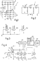
- FIG.1 shows a schematic view of an integrated circuit 1 having a number of pins 2, one of which, indicated by 3, is grounded; clamping diodes 4 between pins 2 and pin 3; and a clamping diode 8 between two pins 2.
- Clamping diodes 4 are formed as shown in Fig.2, which shows a cross section of the chip 5 of integrated circuit 1.
- Fig.2 in which the circuit 1 component layers and sinkers are omitted, shows a P type substrate 6, and the N type sinkers 7 connected to pins 2 and which, together with substrate 6, form PN junctions defining clamping diodes 4.
- the above known system therefore consists in appropriately biasing the clamping diodes and measuring the current through them for detecting any disconnected or short-circuited components.
- diodes 4 are not always known and, at any rate, are not consistent, by virtue of depending closely on the type of external connection of the pins (more specifically, on whether they are connected to external buses or other pins on another integrated circuit) and also on the type of signal for which the pin is designed. As a result, absolute measurement of the current through each pin cannot always be depended on for determining correct connection.
- connection test method of the second type i.e. of straightforward design and circuitry, which nevertheless provides for a high degree of reliability, even in the case of integrated circuits whose internal structure is unknown.
- a method of connection testing electronic boards comprising integrated circuits having pins and clamping diodes between said pins; characterized by the fact that it comprises stages consisting in: identifying uniform groups of said diodes on the basis of functional or structural characteristics, for identifying multiterminal structures; biasing said multiterminal structures so as to cause currents to flow through the terminals of said multiterminal structures; measuring said currents at said terminals; comparing said measured currents; and detecting any faulty connections on the basis of marked variations in said currents.
- the present invention is based on the fact that, on integrated circuits of the above type, various structures are obtainable by appropriately grouping the clamping diodes, that is: a diode structure consisting of a diode between the ground pin and each other pin, or between two different pins; a transistor structure consisting of two diodes between the ground pin and two different pins (the transistors in fact consist more or less of two antiseries PN junctions); a multiemitter structure consisting of the diodes between the ground pin and the other pins, and which present similar functional and connection characteristics; a multicollector structure, as above; an SCR structure consisting of two series diodes, one between ground and a first pin, and the other between the first pin and a second pin (if any) on the integrated circuit.
- Fig.3 shows an equivalent diagram of the clamping diodes in the Fig.1 circuit, grouped uniformly as described above according to the type of pin connection (bus or single component); the type of signals for which the pin is designed (e.g. analog, digital, address, data or control); and the level of the electric quantities involved.
- Each group thus defines a multicollector structure (Fig.3 shows three, 10a, 10b, 10c, respectively relative for example to bus-connected data, address and control signal pins) having its own base terminal 11 (grounded pin), its own emitter terminal 12 (one of the pins in the homogeneous group), and a number of collector terminals 13 (the other pins in the same group).
- each structure 10 is tested by biasing it, measuring the collector current at terminals 13, and checking that the difference in current (which is inevitable, due to production spread and an intrinsic amount of measuring inaccuracy) is below a given percentage of a given reference value.
- each structure 10 is connected to a test apparatus 15 as shown in Fig.4.
- apparatus 15 comprises a current source 16 connected between base terminal 11 and emitter terminal 12; a number of measuring branches 17 connected between emitter terminal 12 and respective collector terminals 13; and a processing logic circuit 18.
- each measuring branch 17 comprises a series-connected voltage source 20 and ammeter 21; and logic circuit 18 comprises an interface 22 connected to ammeters 21 from which it receives the measuring result; a processing unit 23 connected to interface 22 and controlling the diagnostic stage; an input/output unit 24 connected to processing unit 23, for exchanging data, commands and information with the operator or an external system; and a data memory 25.
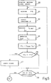
- Fig.5 shows a flow chart of the various stages whereby each integrated circuit is tested according to the present system.
- block 30 provides for acquiring information relative to the diodes grouped uniformly as described above, i.e. connected to similarly connected pins designed for the same type of signal or electric quantity. This may be done by the operator entering the above data on input/output unit 24, or by reading memory 25, if the data has already been entered and stored for similar integrated circuits.
- block 31 then provides for acquiring the permitted percentage deviation of the collector currents in the diodes of the same group, which deviation is selected, for example, on the basis of the absolute value of the measured collector current and/or predictable spread according to the technology of the integrated circuit in question, as well as the type of pin connection and signal.
- Block 32 then provides for enabling current source 16 and sources 20; and block 33 for acquiring, via interface 22, the I Ci current values measured by ammeters 21 and produced by amplifying the base current injected by source 16, and one of which constitutes reference value I C,REF with which the other collector currents are compared.
- the currents so detected are then memorized in block 34 and subsequently compared with one another. More specifically, for all the detected I C values, block 35 provides for calculating the difference DI i between the i-thy current I Ci and reference current I C,REF , and block 36 for checking the differences are below the set deviation percentage V%.
- block 38 checks that all the homogeneous groups on the circuit have been tested. Block 38 is also reached in the event of the connections testing out correctly (NO output of block 36). When all the multicollector structures 10 on circuit 1 have been tested (YES output of block 38), the procedure is terminated (or repeated for other circuits on the same board). Conversely (NO output of block 38), block 38 goes back to block 31.
- connection testing integrated circuit pins by virtue of the collector currents, in the event of correct connection, being comparable and varying within predetermined limits depending on the connection and operating characteristics of the pin, and regardless of the absolute value detected.
- said absolute value need not necessarily be known beforehand, so that the test may also be applied to integrated circuits of unknown function, and of which are known only the connections and the type and level of the electric quantities involved, as shown on any integrated circuit data sheet.
- the homogeneous diode groups constituting the multicollector structures may be acquired automatically; and the procedure described may be implemented in and form only part of a much wider test system.
- collector currents I Ci may be measured sequentially, thus drastically simplifying apparatus 15 by reducing it to a single measuring branch 17, as well as interface unit 22 for acquiring the detected measurements.
- the system may also provide for additional checks, e.g. for detecting faulty connection of the reference base-collector diode or base-emitter diode.
- the collector currents may also be compared differently, by calculating a mean detected current value and comparing each collector current value with the mean value instead of a reference value. Also, the mean value or deviation may be calculated using various techniques as required.
Landscapes
- Engineering & Computer Science (AREA)
- Physics & Mathematics (AREA)
- General Physics & Mathematics (AREA)
- Computer Hardware Design (AREA)
- Microelectronics & Electronic Packaging (AREA)
- General Engineering & Computer Science (AREA)
- Tests Of Electronic Circuits (AREA)
- Testing Of Individual Semiconductor Devices (AREA)
- Testing Or Measuring Of Semiconductors Or The Like (AREA)
- Testing Of Short-Circuits, Discontinuities, Leakage, Or Incorrect Line Connections (AREA)
Applications Claiming Priority (2)
| Application Number | Priority Date | Filing Date | Title |
|---|---|---|---|
| ITTO920463 | 1992-05-29 | ||
| ITTO920463A IT1259395B (it) | 1992-05-29 | 1992-05-29 | Metodo di rilevamento di connesioni erronee in schede elettroniche |
Publications (3)
| Publication Number | Publication Date |
|---|---|
| EP0571963A2 true EP0571963A2 (fr) | 1993-12-01 |
| EP0571963A3 EP0571963A3 (fr) | 1994-04-13 |
| EP0571963B1 EP0571963B1 (fr) | 1998-08-26 |
Family
ID=11410503
Family Applications (1)
| Application Number | Title | Priority Date | Filing Date |
|---|---|---|---|
| EP93108451A Expired - Lifetime EP0571963B1 (fr) | 1992-05-29 | 1993-05-25 | Procédé d'essai des connexions de cartes électroniques |
Country Status (3)
| Country | Link |
|---|---|
| EP (1) | EP0571963B1 (fr) |
| DE (1) | DE69320535T2 (fr) |
| IT (1) | IT1259395B (fr) |
Cited By (4)
| Publication number | Priority date | Publication date | Assignee | Title |
|---|---|---|---|---|
| EP0671689A3 (fr) * | 1994-03-09 | 1995-12-27 | Hewlett Packard Co | Test d'interconnexion par l'utilisation de données de topologie de circuit imprimé. |
| US5521513A (en) * | 1994-10-25 | 1996-05-28 | Teradyne Inc | Manufacturing defect analyzer |
| EP0892274A3 (fr) * | 1997-07-16 | 2000-08-02 | Sharp Kabushiki Kaisha | Système et procédé pour facilement inspecter l'état de la connection d'un composant BGA/CSP à une plaque de support |
| US7385410B2 (en) | 2002-10-29 | 2008-06-10 | Aeroflex International Limited, Of Longacres House | Method of and apparatus for testing for integrated circuit contact defects |
Family Cites Families (3)
| Publication number | Priority date | Publication date | Assignee | Title |
|---|---|---|---|---|
| EP0306656A1 (fr) * | 1987-08-20 | 1989-03-15 | Siemens Aktiengesellschaft | Dispositif pour le test de composants à circuits intégrés |
| US5101152A (en) * | 1990-01-31 | 1992-03-31 | Hewlett-Packard Company | Integrated circuit transfer test device system utilizing lateral transistors |
| DE4110551C1 (fr) * | 1991-03-30 | 1992-07-23 | Ita Ingenieurbuero Fuer Testaufgaben Gmbh, 2000 Hamburg, De |
-
1992
- 1992-05-29 IT ITTO920463A patent/IT1259395B/it active IP Right Grant
-
1993
- 1993-05-25 EP EP93108451A patent/EP0571963B1/fr not_active Expired - Lifetime
- 1993-05-25 DE DE69320535T patent/DE69320535T2/de not_active Expired - Fee Related
Non-Patent Citations (1)
| Title |
|---|
| None |
Cited By (7)
| Publication number | Priority date | Publication date | Assignee | Title |
|---|---|---|---|---|
| EP0671689A3 (fr) * | 1994-03-09 | 1995-12-27 | Hewlett Packard Co | Test d'interconnexion par l'utilisation de données de topologie de circuit imprimé. |
| EP0930570A3 (fr) * | 1994-03-09 | 1999-07-28 | Hewlett-Packard Company | Test d'interconnexion par l'utilisation de données de topologie de circuit imprimé |
| US5521513A (en) * | 1994-10-25 | 1996-05-28 | Teradyne Inc | Manufacturing defect analyzer |
| US5554928A (en) * | 1994-10-25 | 1996-09-10 | Teradyne, Inc. | Manufacturing defect analyzer |
| EP0892274A3 (fr) * | 1997-07-16 | 2000-08-02 | Sharp Kabushiki Kaisha | Système et procédé pour facilement inspecter l'état de la connection d'un composant BGA/CSP à une plaque de support |
| US6288346B1 (en) | 1997-07-16 | 2001-09-11 | Sharp Kabushiki Kaisha | System and method for easily inspecting a bonded state of a BGA/CSP type electronic part to a board |
| US7385410B2 (en) | 2002-10-29 | 2008-06-10 | Aeroflex International Limited, Of Longacres House | Method of and apparatus for testing for integrated circuit contact defects |
Also Published As
| Publication number | Publication date |
|---|---|
| ITTO920463A1 (it) | 1993-11-29 |
| EP0571963A3 (fr) | 1994-04-13 |
| IT1259395B (it) | 1996-03-13 |
| DE69320535T2 (de) | 1999-04-22 |
| ITTO920463A0 (it) | 1992-05-29 |
| DE69320535D1 (de) | 1998-10-01 |
| EP0571963B1 (fr) | 1998-08-26 |
Similar Documents
| Publication | Publication Date | Title |
|---|---|---|
| EP0305148B1 (fr) | Détermination de l'orientation des composants | |
| US5280237A (en) | Method for testing semiconductor integrated circuits soldered to boards and use of a transistor tester for this method | |
| JP7224313B2 (ja) | 電子デバイスを自動テストするための装置及び方法 | |
| EP0292137A2 (fr) | Système pour le contrôle de la transmission d'un circuit intégré | |
| US5521513A (en) | Manufacturing defect analyzer | |
| US4183460A (en) | In-situ test and diagnostic circuitry and method for CML chips | |
| JPH0269684A (ja) | 集積回路の電源線試験方法 | |
| CN211426704U (zh) | 芯片的gpio的自动化测试系统 | |
| US5101152A (en) | Integrated circuit transfer test device system utilizing lateral transistors | |
| EP0295782B1 (fr) | Test du bêta d'un transistor sur circuit et procédé | |
| EP0571963B1 (fr) | Procédé d'essai des connexions de cartes électroniques | |
| US6188235B1 (en) | System and method for verifying proper connection of an integrated circuit to a circuit board | |
| EP0317578A4 (fr) | Testeur de circuits a trois etats. | |
| US11067623B2 (en) | Test system and method of operating the same | |
| KR100311955B1 (ko) | 전자회로의기능테스트장치및방법 | |
| US5414373A (en) | Automatic transistor checker | |
| US5570012A (en) | Apparatus for testing a semiconductor device by comparison with an identical reference device | |
| US6101458A (en) | Automatic ranging apparatus and method for precise integrated circuit current measurements | |
| US3534262A (en) | In-circuit reverse leakage testing of diodes driving associated amplifiers by monitoring changes in amplifier outputs | |
| JPS6371669A (ja) | 電子回路装置の検査方法 | |
| Johnson et al. | Applied power board testing | |
| Campola et al. | Total Ionizing Dose Test of Microsemi's Silicon Switching Transistors JANTXV2N2222AUB and 2N2907AUB | |
| JPH07191079A (ja) | 半導体集積回路の評価方法及び評価治具 | |
| JPH01276638A (ja) | ウエーハの試験方法 | |
| JPH02198372A (ja) | プリント板のアセンブリ接続チェック方法 |
Legal Events
| Date | Code | Title | Description |
|---|---|---|---|
| PUAI | Public reference made under article 153(3) epc to a published international application that has entered the european phase |
Free format text: ORIGINAL CODE: 0009012 |
|
| AK | Designated contracting states |
Kind code of ref document: A2 Designated state(s): DE FR GB |
|
| PUAL | Search report despatched |
Free format text: ORIGINAL CODE: 0009013 |
|
| AK | Designated contracting states |
Kind code of ref document: A3 Designated state(s): DE FR GB |
|
| 17P | Request for examination filed |
Effective date: 19940929 |
|
| 17Q | First examination report despatched |
Effective date: 19970313 |
|
| GRAG | Despatch of communication of intention to grant |
Free format text: ORIGINAL CODE: EPIDOS AGRA |
|
| GRAG | Despatch of communication of intention to grant |
Free format text: ORIGINAL CODE: EPIDOS AGRA |
|
| GRAH | Despatch of communication of intention to grant a patent |
Free format text: ORIGINAL CODE: EPIDOS IGRA |
|
| GRAH | Despatch of communication of intention to grant a patent |
Free format text: ORIGINAL CODE: EPIDOS IGRA |
|
| GRAA | (expected) grant |
Free format text: ORIGINAL CODE: 0009210 |
|
| AK | Designated contracting states |
Kind code of ref document: B1 Designated state(s): DE FR GB |
|
| REF | Corresponds to: |
Ref document number: 69320535 Country of ref document: DE Date of ref document: 19981001 |
|
| ET | Fr: translation filed | ||
| PGFP | Annual fee paid to national office [announced via postgrant information from national office to epo] |
Ref country code: FR Payment date: 19990426 Year of fee payment: 7 |
|
| PGFP | Annual fee paid to national office [announced via postgrant information from national office to epo] |
Ref country code: GB Payment date: 19990524 Year of fee payment: 7 |
|
| PGFP | Annual fee paid to national office [announced via postgrant information from national office to epo] |
Ref country code: DE Payment date: 19990601 Year of fee payment: 7 |
|
| PLBE | No opposition filed within time limit |
Free format text: ORIGINAL CODE: 0009261 |
|
| 26N | No opposition filed | ||
| PG25 | Lapsed in a contracting state [announced via postgrant information from national office to epo] |
Ref country code: GB Free format text: LAPSE BECAUSE OF NON-PAYMENT OF DUE FEES Effective date: 20000525 |
|
| GBPC | Gb: european patent ceased through non-payment of renewal fee |
Effective date: 20000525 |
|
| PG25 | Lapsed in a contracting state [announced via postgrant information from national office to epo] |
Ref country code: FR Free format text: LAPSE BECAUSE OF NON-PAYMENT OF DUE FEES Effective date: 20010131 |
|
| PG25 | Lapsed in a contracting state [announced via postgrant information from national office to epo] |
Ref country code: DE Free format text: LAPSE BECAUSE OF NON-PAYMENT OF DUE FEES Effective date: 20010301 |
|
| REG | Reference to a national code |
Ref country code: FR Ref legal event code: ST |