EP0572294A1 - Eingangssignalbegrenzer für einen Analog-Digital-Wandler - Google Patents
Eingangssignalbegrenzer für einen Analog-Digital-Wandler Download PDFInfo
- Publication number
- EP0572294A1 EP0572294A1 EP19930401181 EP93401181A EP0572294A1 EP 0572294 A1 EP0572294 A1 EP 0572294A1 EP 19930401181 EP19930401181 EP 19930401181 EP 93401181 A EP93401181 A EP 93401181A EP 0572294 A1 EP0572294 A1 EP 0572294A1
- Authority
- EP
- European Patent Office
- Prior art keywords
- analog
- input
- converter
- digital converter
- output
- Prior art date
- Legal status (The legal status is an assumption and is not a legal conclusion. Google has not performed a legal analysis and makes no representation as to the accuracy of the status listed.)
- Withdrawn
Links
- 238000006243 chemical reaction Methods 0.000 claims description 41
- 230000001186 cumulative effect Effects 0.000 claims description 2
- 235000021183 entrée Nutrition 0.000 description 9
- 230000006835 compression Effects 0.000 description 2
- 238000007906 compression Methods 0.000 description 2
- 230000002411 adverse Effects 0.000 description 1
- 238000013459 approach Methods 0.000 description 1
- 230000015556 catabolic process Effects 0.000 description 1
- 230000006378 damage Effects 0.000 description 1
- 230000003247 decreasing effect Effects 0.000 description 1
- 238000006731 degradation reaction Methods 0.000 description 1
- 230000003111 delayed effect Effects 0.000 description 1
- 230000006866 deterioration Effects 0.000 description 1
- 238000002592 echocardiography Methods 0.000 description 1
- 230000007613 environmental effect Effects 0.000 description 1
- 230000035945 sensitivity Effects 0.000 description 1
- 230000001502 supplementing effect Effects 0.000 description 1
Images


Classifications
-
- H—ELECTRICITY
- H03—ELECTRONIC CIRCUITRY
- H03M—CODING; DECODING; CODE CONVERSION IN GENERAL
- H03M1/00—Analogue/digital conversion; Digital/analogue conversion
- H03M1/12—Analogue/digital converters
- H03M1/18—Automatic control for modifying the range of signals the converter can handle, e.g. gain ranging
- H03M1/186—Automatic control for modifying the range of signals the converter can handle, e.g. gain ranging in feedforward mode, i.e. by determining the range to be selected directly from the input signal
- H03M1/187—Automatic control for modifying the range of signals the converter can handle, e.g. gain ranging in feedforward mode, i.e. by determining the range to be selected directly from the input signal using an auxiliary analogue/digital converter
Definitions
- the present invention relates to a device for limiting the input signals of an analog-digital converter.
- a first drawback stems from the deterioration of the linearity of these limiting circuits when the amplitude of the signals which they allow to pass approaches the threshold. limitation. In the case of a radar reception chain for example, this adversely affects the linearity of the reception chain.
- the object of the invention is to overcome the aforementioned drawbacks, in particular by allowing linearity to be maintained over the entire conversion range of the converters.
- the main advantages of the invention are that it makes it possible to extend the conversion range of analog-digital converters, that it is not very sensitive to environmental conditions, that it does not does not require delicate adjustment, finally that it is simple to implement, that it is reliable and that it is inexpensive.
- FIG. 1 shows a curve representative of a signal Se entering for example into an analog-digital converter and having a voltage Ve as a function of time t.
- This signal can for example be that received by a radar reception chain.
- the converter has for example a conversion range delimited by voltages Vc and -Vc, this conversion range could just as easily be delimited between O and Vc, Vc representing a positive voltage, between 5v and 12v by example.
- a voltage greater than Vc or less than -Vc at the input of an analog-digital converter generally destroys the latter.
- the signal Se of FIG. 1 remains within limits L + and L- corresponding respectively to the voltages Vc and -Vc delimiting the conversion range of the converter.
- this signal Se has, for example, intermittent voltage peaks P1, P2, P3, P4, P5, P6 greater than Vc or less than Vc and of greater or lesser absolute value and therefore capable of destroying the converter.
- FIG. 2 shows the transfer function of a limitation circuit according to the prior art.
- This transfer function between the input voltage VLE and the output voltage VLS of the limiting circuit is represented by the curve T.
- the transfer function T Up to a voltage V1E, the transfer function T is substantially linear. Beyond this voltage V1E, this real transfer function T departs from an ideal transfer function T ', linear.
- the two transfer functions T, T ' join an asymptote AL corresponding to the limiting voltage VLO of the circuit.
- This voltage VLO is necessarily less than or equal to the voltage Vc of the analog-digital converter.
- this voltage VLO is set below Vc, or above -Vc with a significant AV voltage deviation to compensate in particular for these drifts.
- this deviation ⁇ V does not make it possible to take full advantage of the conversion range of the analog converter -digital delimited by the voltage Vc.
- FIG. 3 proposes a first example of a device for limiting, according to the invention, an input signal from a converter 1.
- the input of the device E is connected to the input of an auxiliary analog-digital converter 2, comprising for example few conversion bits and having a range delimited by at least one voltage V'c greater than Vc and at the voltages of the input signals.
- the auxiliary converter 2 can be produced for example from discrete elements according to means known to those skilled in the art, and have a few conversion bits; 2, 3 or 4 for example. If the signals to be converted are positive and negative, it can work in addition to 2 to take account of the sign of the signals. It codes for example the multiple voltages, positive or negative, of the voltage Vc defining the conversion range of the main converter 1. Thus, if the input voltage is equal to 3Vc + ⁇ V, ⁇ V being less than Vc, the converter auxiliary 2 displays the digital value at its output 3. In other words, the least significant bit of auxiliary converter 2, denoted LSB, codes the value Vc. However, this least significant bit LSB could code a value different from Vc.
- the auxiliary converter 2 is connected at its output to the input of a digital-analog converter 3 having for example the same number of bits as the auxiliary analog-digital converter 2 as well as the same scale factor, that is to say that is to say that a least significant bit, denoted LSB, of the digital-analog converter corresponds to the coding of an output voltage substantially equal to Vc. Its output is therefore substantially equal to multiples of the voltage Vc delimiting the conversion range of the main converter 1.
- the output of the digital-analog converter 3 is connected to an input of a subtractor circuit 4, the negative input for example.
- the other input of this subtractor circuit 4 is connected to the output a delay circuit 5, the input of which is connected to the input E of the device and to the input of the analog-digital auxiliary converter 2.
- the delay time ⁇ provided by the delay circuit 5 is at least equal to cumulative conversion time of the auxiliary converter 2 and of the digital-analog converter 3.
- the subtractor circuit 4 has at its output a voltage equal to the voltage arriving at its positive input, therefore equal to the input voltage of the device according to the invention , delayed by ⁇ , reduced by the voltage arriving at its negative input, that is to say that leaving the digital-analog converter 3, multiple of the voltage Vc.
- the output S of the subtractor circuit 4 constitutes the output of the device according to the invention, this output S is wired to the input of the main analog-digital converter 1 for which it is necessary to limit the input signal.
- All the signals whose amplitude is less than Vc cause a code equal to O at the output of the auxiliary converter 2 therefore a zero voltage at the negative input of the subtractor circuit 4.
- the output S of the device according to the invention then reproduces at l input of the main converter 1 the signal present at its input E.
- the device is in this case transparent. If the voltage present at the input E of the device is equal for example to 2 q xVc + ⁇ V, ⁇ V being less than Vc and q being less than the number of bits of the auxiliary converter 2, then the output of the latter displays 2 q . Consequently, the output of the digital-analog converter 3 has an output equal to 2 q xVc. This latter voltage is subtracted, via the subtractor circuit 4, from the input signal.
- the signals present at the input of the device according to the invention can be positive or negative since the auxiliary converter 2 and the digital-analog converter 3 can operate in addition to 2.
- the main analog-digital converter 1 can then operate according to a natural binary code, without indication of a sign.
- a flag consisting for example of a combination of the bits of the auxiliary converter 2 is positioned at an agreed logic level when for example one at least of these bits goes to 1, the passage of the least significant bit to 1 indicating for example a limitation of a signal whose voltage passes above Vc and the passage of all the bits to 1 indicating for example a limitation of a signal whose voltage drops below -Vc.
- the limiting device has a linearity over the entire conversion range of the main analog-digital converter 1, in particular at the level of the high amplitude signals inside the conversion range, thus avoiding conversion errors and making it possible to take advantage of the full conversion range of the main converter 1.
- This linearity is in fact that of the auxiliary analog-digital converter 2, of the digital-analog converter 3 and of the subtractor 4 on this conversion range.
- Figure 4 shows a possible device according to the invention very close to the previous one where a sampler-blocker 6 was added as an input, the output of the latter being connected to the inputs of the auxiliary converter 2 and to the delay circuit 5.
- the sampler -blocker 6 allows for example to overcome sudden variations in signals at input E of the device.
- the device of FIG. 5 repeats the device of FIG. 4 by explaining a possible embodiment of the subtractor circuit 4.
- This can consist for example of an operational amplifier 41 and three resistors 42, 43, 44.
- L positive input of the operational amplifier 41 constituting the positive input of the subtractor circuit 4.
- the negative input of the operational amplifier 41 is connected to one of the poles of each of the resistors 42, 43, 44, a resistor 42 having its other pole connected to the ground potential representing the electrical zero of the circuits of the device, a resistor 43 having its other pole connected at the output of the digital-analog converter 3 and constituting the negative input of the subtractor circuit 4, and a resistor 44 having its other pole connected to the output of the operational amplifier 41 constituting the output of the subtractor circuit 4.
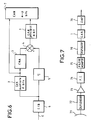
- Figure 6 shows a possible variant of use of the device according to the invention.
- the output bits of the auxiliary analog-digital converter 2 are used to extend the conversion range of the main analog-digital converter 1.
- the latter encodes the part of the multiple voltage of Vc, Vc having been previously defined as being the maximum voltage, limit of the conversion range of the main converter 1, and the latter codes the part added to the voltage coded by the auxiliary converter 2 and of amplitude less than Vc.
- a signal present at the input E of the device according to the invention having a voltage to be converted equal to 2 q Vc + ⁇ V causes a code equal to 2 q at the output of the auxiliary converter 2, coded on p bits, q being less than or equal to p.
- ⁇ V can be coded for example on n bits, by the main converter 1.
- the processing circuits can take into account n + p bits
- the device according to the invention associated with the main converter 1 in addition to the fact that '' it limits the signals present at the input of the latter, makes it possible to obtain the equivalent of an analog-digital converter 7 having n + p bits having a conversion range equal to that of the auxiliary converter 2, that is ie at least equal to 2 P Vc.
- FIG. 7 shows a possible application of the device according to the invention.
- the latter numbered 70, is used for example in a radar reception chain.
- a receiving antenna 71 is connected to a duplexer 72 whose output is coupled to an amplifier 73.
- the output of the latter is connected to circuits 74 for transposing the signal received into so-called intermediate frequencies, of the order of 60 MHz by example.
- the output of these circuits 74 is connected to the input of a suitable filter 75.
- the output of the adapted filter 75 is connected to the input of the device 70 according to the invention whose output voltage is limited for example to the range converting the analog digital converter 1 connected to the output of the device 70.
- the output of the analog digital converter 1 can then be connected to a digital amplitude-phase discriminator.
- the device according to the invention replaces conventional limitation circuits with the aforementioned drawbacks.
- the device according to the invention limits the signals to the input of an analog-digital converter, but it can just as easily limit the signals to the input of other circuits.
- the voltage Vc then being the maximum admissible voltage at the input of these circuits, this voltage constituting the limiting voltage of the device according to the invention.
Landscapes
- Engineering & Computer Science (AREA)
- Theoretical Computer Science (AREA)
- Analogue/Digital Conversion (AREA)
- Tone Control, Compression And Expansion, Limiting Amplitude (AREA)
Applications Claiming Priority (2)
| Application Number | Priority Date | Filing Date | Title |
|---|---|---|---|
| FR9206433 | 1992-05-26 | ||
| FR9206433A FR2691861A1 (fr) | 1992-05-26 | 1992-05-26 | Dispositif de limitation de signaux d'entrée d'un convertisseur analogique-numérique. |
Publications (1)
| Publication Number | Publication Date |
|---|---|
| EP0572294A1 true EP0572294A1 (de) | 1993-12-01 |
Family
ID=9430197
Family Applications (1)
| Application Number | Title | Priority Date | Filing Date |
|---|---|---|---|
| EP19930401181 Withdrawn EP0572294A1 (de) | 1992-05-26 | 1993-05-07 | Eingangssignalbegrenzer für einen Analog-Digital-Wandler |
Country Status (4)
| Country | Link |
|---|---|
| EP (1) | EP0572294A1 (de) |
| JP (1) | JPH077354A (de) |
| CA (1) | CA2096914A1 (de) |
| FR (1) | FR2691861A1 (de) |
Citations (1)
| Publication number | Priority date | Publication date | Assignee | Title |
|---|---|---|---|---|
| US3823376A (en) * | 1970-03-12 | 1974-07-09 | Philips Corp | Transmitter for the transmission of analogue signals by pulse code |
-
1992
- 1992-05-26 FR FR9206433A patent/FR2691861A1/fr active Pending
-
1993
- 1993-05-07 EP EP19930401181 patent/EP0572294A1/de not_active Withdrawn
- 1993-05-25 CA CA 2096914 patent/CA2096914A1/fr not_active Abandoned
- 1993-05-25 JP JP5122667A patent/JPH077354A/ja active Pending
Patent Citations (1)
| Publication number | Priority date | Publication date | Assignee | Title |
|---|---|---|---|---|
| US3823376A (en) * | 1970-03-12 | 1974-07-09 | Philips Corp | Transmitter for the transmission of analogue signals by pulse code |
Non-Patent Citations (2)
| Title |
|---|
| "SUBRANGING ADCS OPERATE AT HIGH SPEED WITH HIGH RESOLUTION.", EDN ELECTRICAL DESIGN NEWS.(TEXAS INSTRUMENT), REED BUSINESS INFORMATION, HIGHLANDS RANCH, CO., US, vol. 36., no. 08., 11 April 1991 (1991-04-11), US, pages 139 - 144 + 146 + 14, XP000225559, ISSN: 0012-7515 * |
| BALASUBRAMANIAN K.: "HIGH-RES A-TO-D USING LOW-RES CONVERTERS.", ELECTRONICS WORLD., NEXUS MEDIA COMMUNICATIONS, SWANLEY, KENT., GB, vol. 97., no. 1669., 1 December 1991 (1991-12-01), GB, pages 1052., XP000255161, ISSN: 0959-8332 * |
Also Published As
| Publication number | Publication date |
|---|---|
| FR2691861A1 (fr) | 1993-12-03 |
| JPH077354A (ja) | 1995-01-10 |
| CA2096914A1 (fr) | 1993-11-27 |
Similar Documents
| Publication | Publication Date | Title |
|---|---|---|
| FR2478904A1 (fr) | Circuit de commande de gain | |
| FR2498396A1 (fr) | Circuit d'arbitrage | |
| EP2201689B1 (de) | Quantisierer, analog-digital-umsetzer mit einem solchen quantisierer und einen solchen umsetzer integrierender ultrabreitbandempfänger | |
| EP0421896B1 (de) | Analog-Digitalwandler von hoher Umwandlungsfrequenz | |
| EP0004815A2 (de) | Verfahren zum Übertragen elektrischer Signale mittels optischer Verbindung und Vorrichtung zur automatischen Verstärkungsregelung eines an der optischen Verbindung gekuppelten Empfangsweges | |
| FR2525006A1 (fr) | Detecteur d'intrusion | |
| EP0359633B1 (de) | Logarithmischer Hüllkurvendetektor für ein analoges Signal | |
| FR2507413A1 (fr) | Convertisseur analogique-numerique ayant un circuit d'auto-polarisation | |
| FR2433862A1 (fr) | Installation de circuits pour la detection d'erreurs dans des signaux numeriques | |
| EP0567380B1 (de) | Verfahren und Vorrichtung zur Kompensation von Phasenschwankungen von einer mit einem Hochfrequenzrohr verstärkten Welle | |
| EP0572294A1 (de) | Eingangssignalbegrenzer für einen Analog-Digital-Wandler | |
| EP1039643A1 (de) | Analog-Digital-Wandleranordnung mit konstanter differentieller nicht-linearität | |
| FR2491275A1 (fr) | Procede de reduction du bruit et de la diaphonie en codage analogique-numerique et codeur correspondant | |
| EP1290869B1 (de) | Verfahren zur umsetzung eines analogen signals in ein digitales signal und elektromagnetsicher strahlungsdetektor welcher dieses verfahren benutzt | |
| EP0404634A1 (de) | Schnittstelle für digitale Schaltungen unterschiedlichen Typs | |
| EP0155046B1 (de) | Gerät zur Digital-Analogwandlung | |
| CA2106268A1 (fr) | Circuit de codage analogique-numerique a compensation automatique du decalage du zero | |
| EP0866562A1 (de) | Analog-Digital-Wandler mit einer Verstärkungskalibriervorrichtung | |
| EP1192718A1 (de) | Verfahren und system zur kompensierung der nichtlinearität eines sigma-delta analog-digital-wandlers | |
| FR2515898A1 (fr) | Procede et dispositif de conversion analogique-numerique de type adaptatif | |
| CA1213006A (fr) | Circuit logique a seuil et a securite intrinseque | |
| EP0055636B1 (de) | Abweichungsempfänger für Sekundärradar | |
| CA2347164A1 (fr) | Compensation du retard du convertisseur analogique-numerique dans les modulateurs sigma-delta | |
| CA1257394A (fr) | Balance a poids etalonne et convertisseur analogique numerique utilisant une telle balance | |
| EP0130646A1 (de) | Synchronisierter Komparator |
Legal Events
| Date | Code | Title | Description |
|---|---|---|---|
| PUAI | Public reference made under article 153(3) epc to a published international application that has entered the european phase |
Free format text: ORIGINAL CODE: 0009012 |
|
| AK | Designated contracting states |
Kind code of ref document: A1 Designated state(s): BE CH DE DK ES FR GB IT LI LU SE |
|
| RAP3 | Party data changed (applicant data changed or rights of an application transferred) |
Owner name: THOMSON-CSF |
|
| 17P | Request for examination filed |
Effective date: 19940117 |
|
| 17Q | First examination report despatched |
Effective date: 19960129 |
|
| STAA | Information on the status of an ep patent application or granted ep patent |
Free format text: STATUS: THE APPLICATION IS DEEMED TO BE WITHDRAWN |
|
| 18D | Application deemed to be withdrawn |
Effective date: 19960611 |