EP0572777B1 - Dispositif d'affichage cathodoluminescent et procédé de fabrication - Google Patents
Dispositif d'affichage cathodoluminescent et procédé de fabrication Download PDFInfo
- Publication number
- EP0572777B1 EP0572777B1 EP93105119A EP93105119A EP0572777B1 EP 0572777 B1 EP0572777 B1 EP 0572777B1 EP 93105119 A EP93105119 A EP 93105119A EP 93105119 A EP93105119 A EP 93105119A EP 0572777 B1 EP0572777 B1 EP 0572777B1
- Authority
- EP
- European Patent Office
- Prior art keywords
- cathodoluminescent
- diamond crystallites
- disposed
- display apparatus
- supporting substrate
- Prior art date
- Legal status (The legal status is an assumption and is not a legal conclusion. Google has not performed a legal analysis and makes no representation as to the accuracy of the status listed.)
- Expired - Lifetime
Links
Images


Classifications
-
- H—ELECTRICITY
- H01—ELECTRIC ELEMENTS
- H01J—ELECTRIC DISCHARGE TUBES OR DISCHARGE LAMPS
- H01J1/00—Details of electrodes, of magnetic control means, of screens, or of the mounting or spacing thereof, common to two or more basic types of discharge tubes or lamps
- H01J1/02—Main electrodes
- H01J1/30—Cold cathodes, e.g. field-emissive cathode
- H01J1/304—Field-emissive cathodes
- H01J1/3042—Field-emissive cathodes microengineered, e.g. Spindt-type
-
- H—ELECTRICITY
- H01—ELECTRIC ELEMENTS
- H01J—ELECTRIC DISCHARGE TUBES OR DISCHARGE LAMPS
- H01J31/00—Cathode ray tubes; Electron beam tubes
- H01J31/08—Cathode ray tubes; Electron beam tubes having a screen on or from which an image or pattern is formed, picked up, converted, or stored
- H01J31/10—Image or pattern display tubes, i.e. having electrical input and optical output; Flying-spot tubes for scanning purposes
- H01J31/12—Image or pattern display tubes, i.e. having electrical input and optical output; Flying-spot tubes for scanning purposes with luminescent screen
- H01J31/123—Flat display tubes
- H01J31/125—Flat display tubes provided with control means permitting the electron beam to reach selected parts of the screen, e.g. digital selection
- H01J31/127—Flat display tubes provided with control means permitting the electron beam to reach selected parts of the screen, e.g. digital selection using large area or array sources, i.e. essentially a source for each pixel group
-
- H—ELECTRICITY
- H01—ELECTRIC ELEMENTS
- H01J—ELECTRIC DISCHARGE TUBES OR DISCHARGE LAMPS
- H01J2201/00—Electrodes common to discharge tubes
- H01J2201/30—Cold cathodes
- H01J2201/304—Field emission cathodes
- H01J2201/30403—Field emission cathodes characterised by the emitter shape
-
- H—ELECTRICITY
- H01—ELECTRIC ELEMENTS
- H01J—ELECTRIC DISCHARGE TUBES OR DISCHARGE LAMPS
- H01J2201/00—Electrodes common to discharge tubes
- H01J2201/30—Cold cathodes
- H01J2201/304—Field emission cathodes
- H01J2201/30446—Field emission cathodes characterised by the emitter material
- H01J2201/30453—Carbon types
- H01J2201/30457—Diamond
Definitions
- the present invention relates generally to cathodoluminescent displays and more particularly to flat displays employing a plurality of electron sources.
- the invention relates also to a method for forming a cathodoluminescent display apparatus.
- Cathodoluminescent displays are known in the art and commonly employed as image display devices and light sources.
- visible light is generated in the device by means of photon emission induced by energetic electrons impinging on and in a layer of cathodoluminescent material disposed within the device.
- cathodoluminescent displays require an attendant source of electrons emitted from the electron source and accelerated by an applied anode voltage toward the cathodoluminescent material (phosphor).
- thermal energy is provided to raise the energy level of electrons disposed in an electron emitter above that of the associated vacuum energy barrier so that electrons may be liberated to the free space region adjacent to the electron emitter and, subsequently, accelerated toward the anode on which the phosphor is disposed.
- Electron sources so formed and realized suffer from a number of undesirable features including poor efficiency, large size, lack of integrability, and inability to be incorporated into memory capable image display devices.
- An alternative prior art cathodoluminescent display electron source employs electric field induced electron emission.
- Such prior art electron emitters utilize the electric field enhancing properties of structures formed with geometric discontinuities of small radius of curvature (on the order of 5.10 ⁇ 8m (500 Angstroms) or less) such as tips and sharp edges/wedges to achieve enhanced electric fields on the order of tens of millions of volts per centimeter (>3 x 10⁷V/cm).
- An improvement over other prior art electron source methods is that this technique provides for integrability, small size, and application to memory capable devices.
- cathodoluminescent display devices realized with electric field enhanced electron emitters employing features with geometric discontinuities of small radius of curvature, is that the fabrication methods and structures so formed are undesirably complex and limit the utility of this technique.
- cathodoluminescent display apparatus including a supporting substrate having a major surface and a plurality of diamond crystallites, for emitting electrons, disposed in a random orientation on at least a part of the major surface of the supporting substrate, an insulator layer disposed on an exposed part of the major surface of the supporting substrate and further disposed on some of the diamond crystallites and having a plurality of apertures defined therethrough, a control electrode disposed on the insulator layer and substantially peripherally about at least a part of some of the apertures, and an anode, for collecting any emitted electrons and including a substantially optically transparent faceplate, a substantially optically transparent conductive layer disposed on the faceplate, and a cathodoluminescent layer disposed on the conductive layer, all in fixed space relationship and distally disposed with respect to the electron emitting diamond crystallites, such that upon application of an externally provided voltage between the optically transparent conductive layer and the supporting substrate, electron
- EP-A-0 555 074 in a prior art document according to Article 54(3)Epc is an apparatus which differs from the in claim 1 claimed apparatus in that the diamond crystallites have not a random orientation as claimed now but have a preferred orientation.
- FIGS. 1 - 3 are partial cross-sectional representations of structures realized by performing various steps of a method in accordance with the present invention.
- FIGS. 4 - 6 are partial cross-sectional representations of structures realized by performing various steps of another method in accordance with the present invention.
- FIG. 7 is a partial cross-sectional representation of an embodiment of display apparatus in accordance with the present invention.
- FIG. 8 is a partial cross-sectional representation of another embodiment of display apparatus in accordance with the present invention.
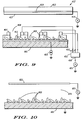
- FIG. 9 is a partial cross-sectional representation of the embodiment of display apparatus illustrated in FIG. 8, rotated 90 degrees
- FIG. 10 is a partial cross sectional view of an embodiment of a structure employing an electron source in accordance with the present invention.
- FIG. 1 there is shown a partial cross sectional depiction of a plurality of electron sources (electron emitters) which are realized by performing a method in accordance with the present invention.
- the method generally includes the steps of providing a supporting substrate 101 having a major surface and disposing thereon a plurality of substantially randomly oriented diamond crystallites 103.
- FIG. 2 is a partial cross-sectional representation of an embodiment of a structure 100 realized by performing the steps described above and further including the steps of depositing an insulator layer 105 on any exposed part of the major surface of supporting substrate 101 and on the plurality of diamond crystallites 103 and depositing a control electrode 107 on insulator layer 105.
- control electrode 107 desirably is conductive/semiconductive material.
- FIG. 3 depicts a partial cross-sectional representation of structure 100 having undergone the further steps of selectively removing some of the material of control electrode 107, selectively removing some of the material of insulator layer 105 such that a plurality of apertures 109 are defined therethrough exposing at least some of the plurality of diamond crystallites, and selectively removing some other material of control electrode 107 such that a plurality of discrete regions forming a plurality of control electrodes are realized each of which is disposed substantially peripherally about at least some of the apertures 109.
- pluralities of electron sources realized in accordance with the method described above may employ a single control electrode extending substantially about each of the plurality of apertures in which instances the step of selectively removing material of the control electrode to form a plurality of control electrodes need not be performed.
- Still other embodiments of an electron source may employ structures, formed in accordance with the method described herein and realizing a single aperture formed through the extent of the control electrode and insulator layer.
- the cross sectional depiction is easily seen to include a plurality of electron sources 110 each of which is situated within an aperture 109 and peripherally bounded by a control electrode 107.
- the control electrodes of FIG. 3 may be considered as selectively formed stripes, observed in end view, each of which has at least an aperture formed therethrough in correspondence with apertures 109 formed through insulator layer 105.
- FIG. 10 depicts an electron source constructed in accordance with the present invention including the structure described previously with reference to FIG. 1 and wherein features first detailed in FIG. 1 are similarly referenced beginning with the numeral "6".
- a supporting substrate 601 being comprised of conductive/semiconductive material is operably coupled to a reference potential, herein depicted as ground potential.
- An electric field is induced at the surfaces of a plurality of diamond crystallites 603 by means of an externally provided voltage source 621 operably coupled to a distally disposed anode 623. So configured, diamond crystallites 603 (electron sources) emit electrons into a free space region 625 immediately adjacent to diamond crystallites 603, which emitted electrons are accelerated toward the anode by the induced electric field.
- FIGS. 4 - 6 are cross-sectional representations of structures realized by performing various steps in accordance with another method of the present invention.
- a plurality of conductive/semiconductive paths 211 are selectively deposited onto the major surface of a supporting substrate 201.
- a plurality of randomly oriented diamond crystallites 203 are then deposited on the conductive/semiconductive paths 211.
- Electron sources realized in accordance with the method of FIGS. 4 - 6 desirably employes a non-conductive supporting substrate 201 to advantageously utilize the selectivity feature provided for by the addition of the plurality of conductive/semiconductive paths 211 on which the plurality of diamond crystallites 203 are disposed.
- FIG. 5 is a partial cross-sectional representation of a structure 200 realized by performing the steps described above and further including the steps of depositing an insulator layer 205 on any exposed part of the major surface of the supporting substrate 201 and on the plurality of diamond crystallites 203 and depositing a control electrode 207 on insulator layer 205.
- control electrode 207 desirably is conductive/semiconductive material.
- FIG. 6 depicts a partial cross-sectional representation of structure 200 having undergone the further steps of selectively removing some of the material of control electrode 207, selectively removing some of the material of insulator layer 205 such that a plurality of apertures 209 are defined therethrough exposing at least some of the plurality of diamond crystallites.
- FIG. 6 depicts a plurality of electron sources 110, each including those exposed diamond crystallites 203 associated with an aperture 209. Further, the plurality of conductive/semiconductive paths 211 are illustrated in end view and substantially orthogonal with respect to control electrode 207, which are represent as a plurality of control electrodes in side view. So described, the structure of FIG.
- the 6 is includes a plurality of electron sources each of which is selectively energized and controlled by means of a matrix of addressing lines comprised of a plurality of conductive/semiconductive paths on which diamond crystallites are disposed and a plurality of control electrodes.
- the electron sources realized in accordance with the methods of FIGS. 1 - 3 and FIGS. 4 - 6, are improvements over methods and structures of the prior art since they do not employ complex formation processes such as sub-micron lithography and highly directional multiple material evaporation techniques necessary to realize electric field enhanced electron emitters.
- the deposition of the plurality of randomly oriented diamond crystallites may be effected by any of many commonly known methods such as, for example, the method employed to manufacture data recording media wherein an oxide material is deposited onto a substrate material and subsequently passed beneath a doctor blade to thin the material to a prescribed thickness.
- FIG. 7 is a cross-sectional depiction of an embodiment of display apparatus 300 in accordance with the present invention.
- a supporting substrate 301 having a major surface on which is disposed a plurality of randomly oriented diamond crystallites 303 is employed as an electron source (electron emitter).
- An anode 312 is provided and positioned distally in fixed space relationship with respect to the plurality of diamond crystallites 303.
- Anode 312 includes a substantially optically transparent faceplate 313 having disposed thereon a substantially optically transparent conductive layer 315 on which is disposed a cathodoluminescent layer 317.
- An externally provided voltage source 319 is operably coupled between supporting substrate 301 and substantially optically transparent conductive layer 315.
- An electric field is induced in the interspace between distally disposed anode 312 and diamond crystallites 303 by virtue of voltage source 319.
- the electric field causes electrons to be emitted from diamond crystallites 303 into a free space region 327, which electrons are accelerated by the electric field toward anode 312.
- Electrons reaching anode 312 excite photon emission in and from cathodoluminescent layer 317 prior to being collected at optically transparent conductive layer 315.
- the electron source in concert with the provided anode, comprise a cathodoluminescent display apparatus.
- Apparatus 400 further includes a first externally provided voltage source 419 operably connected between substantially optically transparent conductive layer 415 of anode 412 and a reference potential, herein depicted as ground potential.
- a second externally provided voltage source 421 is operably coupled between control electrode 407 and the reference potential. It will of course be understood that voltage source 421 can be provided in a variety of configurations including fixed and/or variable voltage sources.
- a plurality of controlled current sources 423 are each operably coupled between a conductive/semiconductive path of the plurality of conductive/semiconductive paths 411 and a reference potential. So formed and operably connected to the externally provided sources, apparatus 400 is an image display apparatus wherein electron emission is co-incidently controlled by a combination of the voltage(s) applied to the control electrode(s) and controlled electron current provided through controlled current sources 423.
- FIG. 9 is a cross sectional view of the embodiment of image display apparatus 400, as described previously with reference to FIG. 8, rotated 90 degrees so that the plurality of control electrodes 407 are depicted in end view and the plurality of conductive/semiconductive paths 411 are depicted in side view.
- An externally provided switch 431 having a plurality of output terminals 433 and an input terminal 435 is shown. Output terminals 433 are operably coupled to the plurality of control electrodes 407.
- Voltage source 421 is operably coupled to input terminal 435 of switch 431.
- Switch 431 is realized by any of many commonly known means including mechanical or electronic devices and may provide functions which include, for example, selective division or reduction of the applied external voltage.
- Switch 431 is employed to apply an appropriate enabling voltage to a selected control electrode of the plurality of control electrodes 407 in a scanning or sequential mode.
- the controlled current sources 423 coupled to each of the conductive/semiconductive paths 411 source an electron current, to be emitted by the corresponding electron source associated with a particular control electrode and conductive/semiconductive path. Electrons emitted from each of the plurality of electron sources selectively energize a part of cathodoluminescent layer 417 as prescribed by the controlled current source and control electrode to provide an image which may be observed through substantially optically transparent faceplate 413.
- a particular electron source and associated part of cathodoluminescent layer 417 which the particular electron source energizes is known as a picture element (pixel).
- An image is comprised of a plurality of picture elements and in the instance of the present disclosure each picture element is comprised of an electron source realized in accordance with the present invention.
- the electron sources realized in accordance with the methods of FIGS. 1 - 3 and FIGS. 4 - 6, and employed in the apparatus of FIG. 9 are improvements over methods and structures of the prior art since they do not employ complex formation processes such as sub-micron lithography and highly directional multiple material evaporation techniques necessary to realize electric field enhanced electron emitters. Further, due to the complex fabrication processes of the prior art it is not possible to realize large cathodoluminescent display structures, other than thermionic cathode ray tube structures, on the order of more than 645 cm (100 square inches)
Landscapes
- Cathode-Ray Tubes And Fluorescent Screens For Display (AREA)
- Cold Cathode And The Manufacture (AREA)
- Electrodes For Cathode-Ray Tubes (AREA)
- Illuminated Signs And Luminous Advertising (AREA)
Claims (9)
- Dispositif d'affichage cathodoluminescent comportant un substrat formant support (401) ayant une surface principale et caractérisé par:- une pluralité de cristallites de diamant (403) pour émettre des électrons, disposées avec une orientation aléatoire sur la surface principale du substrat formant support;- une couche isolante (405) disposée sur toutes les parties exposées de la surface principale du substrat formant support et disposée en outre sur les cristallites de diamant;- une pluralité d'ouvertures (409) définies dans la couche isolante et s'étendant à travers celle-ci;- une électrode de commande (407) disposée sur la couche isolante et sensiblement périphériquement autour de la pluralité d'ouvertures; et- une anode (412) pour recueillir les électrons émis, comprenant une plaque frontale sensiblement transparente optiquement (413), une couche conductrice sensiblement transparente optiquement (415) disposée sur la plaque frontale, et une couche cathodoluminescente (417) disposée sur la couche conductrice, toutes dans une relation spatiale fixe et disposées distalement par rapport aux cristallites de diamant émettant des électrons, de manière que lors de l'application d'une tension (419) entre la couche conductrice sensiblement transparente optiquement et le substrat formant support, des électrons soient émis par les cristallites de diamant et recueillis au niveau de la couche conductrice sensiblement transparente optiquement après avoir d'abord traversé l'épaisseur de la couche cathodoluminescente et avoir comuniqué de l'énergie à celle-ci pour induire l'émission de photons.
- Dispositif d'affichage cathodoluminescent selon la revendication 1, caractérisé en outre par une pluralité de chemins conducteurs ou semiconducteurs (411) disposés sur la surface principale du substrat formant support, la pluralité de cristallites de diamant étant disposées avec une orientation aléatoire sur la pluralité de chemins conducteurs ou semiconducteurs.
- Dispositif d'affichage cathodoluminescent selon la revendication 2, caractérisé en outre par une pluralité d'électrodes de commande (407) disposées chacune sur la couche isolante et sensiblement périphériquement autour d'au moins une partie des ouvertures.
- Dispositif d'affichage cathodoluminescent selon la revendication 3, caractérisé en outre par une source de courant constant commandé (423) connectée fonctionnellement entre un chemin conducteur ou semiconducteur de la pluralité de chemins conducteurs ou semiconducteurs de manière qu'en appliquant sélectivement une tension (419) à la couche conductrice sensiblement transparente optiquement et en fournissant un courant commandé à la pluralité de chemins conducteurs ou semiconducteurs et en fournissant des tensions (421) à la pluralité d'électrodes de commande, une émission d'électrons soit induite à partir de cristallites de la pluralité de cristallites de diamant et les électrons ensuite ensuite recueillis au niveau de la couche conductrice sensiblement transparente optiquement après avoir d'abord traversé l'épaisseur de la couche cathodoluminescente et lui avoir communiqué de l'énergie pour induire l'émission d'électrons.
- Dispositif d'affichage cathodoluminescent selon la revendication 1, caractérisé en outre par une pluralité d'éléments d'image dont chacun comprend certaines cristallites de la pluralité de cristallites de diamant, pour émettre des électrons, et des sources de tension et de courant commandé pour exciter indépendamment chaque élément de la pluralité d'éléments d'image, de manière que toute émission d'électrons par des cristallites de diamant de chaque élément d'image de la pluralité d'éléments d'image excite la couche cathodoluminescente correspondante associée à l'élément d'image dans une mesure déterminée par la source de courant pour produire une image.
- Procédé pour former un dispositif d'affichage cathodoluminescent, comportant l'étape consistant à prévoir un substrat formant support (401) ayant une surface principale et caractérisé par l'étape consistant à:- déposer une pluralité de cristallites de diamant (403) orientées sensiblement au hasard sur au moins une partie de la surface principale du substrat formant support.
- Procédé pour former un dispositif d'affichage cathodoluminescent selon la revendication 6, dans lequel l'étape de dépôt est en outre caractérisée par le dépôt d'une pluralité de chemins conducteurs ou semiconducteurs (411) sur la surface du substrat formant support et le dépôt de la pluralité de cristallites de diamant (403) orientées sensiblement au hasard sur la pluralité de chemins conducteurs ou semiconducteurs.
- Procédé pour former un dispositif d'affichage cathodoluminescent selon la revendication 6, caractérisé en outre par l'étape consistant à déposer une couche isolante (405) sur toute partie exposée de la surface principale du substrat formant support et sur la pluralité de cristallites.
- Procédé pour former un dispositif d'affichage cathodoluminescent selon la revendication 8, caractérisé en outre par l'étape consistant à déposer une pluralité d'électrodes de commande (407) sur la couche isolante et enlever sélectivement une partie de la matière de chacune des électrodes de commande et de la couche isolante pour définir une pluralité d'ouvertures (409) à travers celle-ci pour exposer les cristallites de diamant de la pluralité de cristallites de diamant.
Applications Claiming Priority (2)
| Application Number | Priority Date | Filing Date | Title |
|---|---|---|---|
| US891004 | 1992-06-01 | ||
| US07/891,004 US5278475A (en) | 1992-06-01 | 1992-06-01 | Cathodoluminescent display apparatus and method for realization using diamond crystallites |
Publications (2)
| Publication Number | Publication Date |
|---|---|
| EP0572777A1 EP0572777A1 (fr) | 1993-12-08 |
| EP0572777B1 true EP0572777B1 (fr) | 1996-01-10 |
Family
ID=25397455
Family Applications (1)
| Application Number | Title | Priority Date | Filing Date |
|---|---|---|---|
| EP93105119A Expired - Lifetime EP0572777B1 (fr) | 1992-06-01 | 1993-03-29 | Dispositif d'affichage cathodoluminescent et procédé de fabrication |
Country Status (4)
| Country | Link |
|---|---|
| US (1) | US5278475A (fr) |
| EP (1) | EP0572777B1 (fr) |
| JP (1) | JPH0635405A (fr) |
| DE (1) | DE69301275T2 (fr) |
Families Citing this family (52)
| Publication number | Priority date | Publication date | Assignee | Title |
|---|---|---|---|---|
| US5536193A (en) | 1991-11-07 | 1996-07-16 | Microelectronics And Computer Technology Corporation | Method of making wide band gap field emitter |
| US5763997A (en) | 1992-03-16 | 1998-06-09 | Si Diamond Technology, Inc. | Field emission display device |
| US5543684A (en) | 1992-03-16 | 1996-08-06 | Microelectronics And Computer Technology Corporation | Flat panel display based on diamond thin films |
| US5679043A (en) | 1992-03-16 | 1997-10-21 | Microelectronics And Computer Technology Corporation | Method of making a field emitter |
| US5449970A (en) | 1992-03-16 | 1995-09-12 | Microelectronics And Computer Technology Corporation | Diode structure flat panel display |
| US5675216A (en) | 1992-03-16 | 1997-10-07 | Microelectronics And Computer Technololgy Corp. | Amorphic diamond film flat field emission cathode |
| US6127773A (en) | 1992-03-16 | 2000-10-03 | Si Diamond Technology, Inc. | Amorphic diamond film flat field emission cathode |
| US5686791A (en) | 1992-03-16 | 1997-11-11 | Microelectronics And Computer Technology Corp. | Amorphic diamond film flat field emission cathode |
| CA2152472A1 (fr) * | 1992-12-23 | 1994-07-07 | Nalin Kumar | Ecran plat a triodes dote de cathodes a emission par effet de champ plates |
| US5965971A (en) * | 1993-01-19 | 1999-10-12 | Kypwee Display Corporation | Edge emitter display device |
| US5564959A (en) * | 1993-09-08 | 1996-10-15 | Silicon Video Corporation | Use of charged-particle tracks in fabricating gated electron-emitting devices |
| US7025892B1 (en) | 1993-09-08 | 2006-04-11 | Candescent Technologies Corporation | Method for creating gated filament structures for field emission displays |
| US5559389A (en) * | 1993-09-08 | 1996-09-24 | Silicon Video Corporation | Electron-emitting devices having variously constituted electron-emissive elements, including cones or pedestals |
| US5462467A (en) * | 1993-09-08 | 1995-10-31 | Silicon Video Corporation | Fabrication of filamentary field-emission device, including self-aligned gate |
| EP0727057A4 (fr) | 1993-11-04 | 1997-08-13 | Microelectronics & Computer | Procedes de fabrication de systemes et composants d'affichage a ecran plat |
| DE69432174T2 (de) * | 1993-11-24 | 2003-12-11 | Tdk Corp., Tokio/Tokyo | Kaltkathoden-elektrodenquellenelement und verfahren zur herstellung desselben |
| EP0675519A1 (fr) * | 1994-03-30 | 1995-10-04 | AT&T Corp. | Appareil comprenant des émetteurs à effet de champ |
| US5608283A (en) * | 1994-06-29 | 1997-03-04 | Candescent Technologies Corporation | Electron-emitting devices utilizing electron-emissive particles which typically contain carbon |
| US5552659A (en) * | 1994-06-29 | 1996-09-03 | Silicon Video Corporation | Structure and fabrication of gated electron-emitting device having electron optics to reduce electron-beam divergence |
| US6204834B1 (en) | 1994-08-17 | 2001-03-20 | Si Diamond Technology, Inc. | System and method for achieving uniform screen brightness within a matrix display |
| US5504385A (en) * | 1994-08-31 | 1996-04-02 | At&T Corp. | Spaced-gate emission device and method for making same |
| US5531880A (en) * | 1994-09-13 | 1996-07-02 | Microelectronics And Computer Technology Corporation | Method for producing thin, uniform powder phosphor for display screens |
| EP0706196B1 (fr) * | 1994-10-05 | 2000-03-01 | Matsushita Electric Industrial Co., Ltd. | Cathode émittrice d'électrons; un dispositif d'émission d'électrons, un dispositif d'affichage plat, dispositif de refroidissement thermoélectrique la contenant; et procédé pour la fabrication de la cathode émittrice d'électrons |
| US5623180A (en) * | 1994-10-31 | 1997-04-22 | Lucent Technologies Inc. | Electron field emitters comprising particles cooled with low voltage emitting material |
| US5637950A (en) * | 1994-10-31 | 1997-06-10 | Lucent Technologies Inc. | Field emission devices employing enhanced diamond field emitters |
| FR2726689B1 (fr) * | 1994-11-08 | 1996-11-29 | Commissariat Energie Atomique | Source d'electrons a effet de champ et procede de fabrication de cette source, application aux dispositifs de visualisation par cathodoluminescence |
| US5592053A (en) * | 1994-12-06 | 1997-01-07 | Kobe Steel Usa, Inc. | Diamond target electron beam device |
| US5709577A (en) * | 1994-12-22 | 1998-01-20 | Lucent Technologies Inc. | Method of making field emission devices employing ultra-fine diamond particle emitters |
| US5616368A (en) * | 1995-01-31 | 1997-04-01 | Lucent Technologies Inc. | Field emission devices employing activated diamond particle emitters and methods for making same |
| JPH08273560A (ja) * | 1995-03-30 | 1996-10-18 | Sony Corp | ディスプレイ装置及びディスプレイ装置の駆動方法 |
| US5578906A (en) * | 1995-04-03 | 1996-11-26 | Motorola | Field emission device with transient current source |
| US6296740B1 (en) | 1995-04-24 | 2001-10-02 | Si Diamond Technology, Inc. | Pretreatment process for a surface texturing process |
| US5628659A (en) * | 1995-04-24 | 1997-05-13 | Microelectronics And Computer Corporation | Method of making a field emission electron source with random micro-tip structures |
| US5679895A (en) * | 1995-05-01 | 1997-10-21 | Kobe Steel Usa, Inc. | Diamond field emission acceleration sensor |
| US5713775A (en) * | 1995-05-02 | 1998-02-03 | Massachusetts Institute Of Technology | Field emitters of wide-bandgap materials and methods for their fabrication |
| US5703380A (en) * | 1995-06-13 | 1997-12-30 | Advanced Vision Technologies Inc. | Laminar composite lateral field-emission cathode |
| US5647998A (en) * | 1995-06-13 | 1997-07-15 | Advanced Vision Technologies, Inc. | Fabrication process for laminar composite lateral field-emission cathode |
| US5616061A (en) * | 1995-07-05 | 1997-04-01 | Advanced Vision Technologies, Inc. | Fabrication process for direct electron injection field-emission display device |
| US5644190A (en) * | 1995-07-05 | 1997-07-01 | Advanced Vision Technologies, Inc. | Direct electron injection field-emission display device |
| DE69607356T2 (de) * | 1995-08-04 | 2000-12-07 | Printable Field Emitters Ltd., Hartlepool | Feldelektronenemitterende materialen und vorrichtungen |
| US5990619A (en) * | 1996-03-28 | 1999-11-23 | Tektronix, Inc. | Electrode structures for plasma addressed liquid crystal display devices |
| DE19613713C1 (de) * | 1996-03-29 | 1997-08-21 | Fraunhofer Ges Forschung | Verfahren zur Herstellung von Feldemissionselektronenquellen, so hergestellte Feldemissionselektronenquelle und ihre Verwendung |
| US5729094A (en) * | 1996-04-15 | 1998-03-17 | Massachusetts Institute Of Technology | Energetic-electron emitters |
| EP0974156B1 (fr) * | 1996-06-25 | 2004-10-13 | Vanderbilt University | Structures, reseaux et dispositifs a emission de champ sous vide a micro-pointe et techniques de fabrication |
| US6356014B2 (en) * | 1997-03-27 | 2002-03-12 | Candescent Technologies Corporation | Electron emitters coated with carbon containing layer |
| US6064148A (en) * | 1997-05-21 | 2000-05-16 | Si Diamond Technology, Inc. | Field emission device |
| US6208072B1 (en) | 1997-08-28 | 2001-03-27 | Matsushita Electronics Corporation | Image display apparatus with focusing and deflecting electrodes |
| JP3457162B2 (ja) | 1997-09-19 | 2003-10-14 | 松下電器産業株式会社 | 画像表示装置 |
| US6630782B1 (en) | 1997-12-01 | 2003-10-07 | Matsushita Electric Industrial Co., Ltd. | Image display apparatus having electrodes comprised of a frame and wires |
| US6236381B1 (en) | 1997-12-01 | 2001-05-22 | Matsushita Electronics Corporation | Image display apparatus |
| US6278235B1 (en) | 1997-12-22 | 2001-08-21 | Matsushita Electronics Corporation | Flat-type display apparatus with front case to which grid frame with extended electrodes fixed thereto is attached |
| JPH11213866A (ja) | 1998-01-22 | 1999-08-06 | Sony Corp | 電子放出装置及びその製造方法並びにこれを用いた表示装置 |
Citations (1)
| Publication number | Priority date | Publication date | Assignee | Title |
|---|---|---|---|---|
| EP0555074A1 (fr) * | 1992-02-05 | 1993-08-11 | Motorola, Inc. | Source d'électrons pour dispositif émetteur d'électrons en mode d'appauvrissement |
Family Cites Families (6)
| Publication number | Priority date | Publication date | Assignee | Title |
|---|---|---|---|---|
| FR2593953B1 (fr) * | 1986-01-24 | 1988-04-29 | Commissariat Energie Atomique | Procede de fabrication d'un dispositif de visualisation par cathodoluminescence excitee par emission de champ |
| JPH0275902A (ja) * | 1988-09-13 | 1990-03-15 | Seiko Instr Inc | ダイヤモンド探針及びその成形方法 |
| US5019003A (en) * | 1989-09-29 | 1991-05-28 | Motorola, Inc. | Field emission device having preformed emitters |
| US5138237A (en) * | 1991-08-20 | 1992-08-11 | Motorola, Inc. | Field emission electron device employing a modulatable diamond semiconductor emitter |
| US5129850A (en) * | 1991-08-20 | 1992-07-14 | Motorola, Inc. | Method of making a molded field emission electron emitter employing a diamond coating |
| US5180951A (en) * | 1992-02-05 | 1993-01-19 | Motorola, Inc. | Electron device electron source including a polycrystalline diamond |
-
1992
- 1992-06-01 US US07/891,004 patent/US5278475A/en not_active Expired - Lifetime
-
1993
- 1993-03-29 DE DE69301275T patent/DE69301275T2/de not_active Expired - Fee Related
- 1993-03-29 EP EP93105119A patent/EP0572777B1/fr not_active Expired - Lifetime
- 1993-04-14 JP JP11101893A patent/JPH0635405A/ja active Pending
Patent Citations (1)
| Publication number | Priority date | Publication date | Assignee | Title |
|---|---|---|---|---|
| EP0555074A1 (fr) * | 1992-02-05 | 1993-08-11 | Motorola, Inc. | Source d'électrons pour dispositif émetteur d'électrons en mode d'appauvrissement |
Also Published As
| Publication number | Publication date |
|---|---|
| EP0572777A1 (fr) | 1993-12-08 |
| JPH0635405A (ja) | 1994-02-10 |
| DE69301275T2 (de) | 1996-08-22 |
| US5278475A (en) | 1994-01-11 |
| DE69301275D1 (de) | 1996-02-22 |
Similar Documents
| Publication | Publication Date | Title |
|---|---|---|
| EP0572777B1 (fr) | Dispositif d'affichage cathodoluminescent et procédé de fabrication | |
| US5140219A (en) | Field emission display device employing an integral planar field emission control device | |
| US5528103A (en) | Field emitter with focusing ridges situated to sides of gate | |
| US5445550A (en) | Lateral field emitter device and method of manufacturing same | |
| US5473218A (en) | Diamond cold cathode using patterned metal for electron emission control | |
| EP0528390A1 (fr) | Dispositif électronique à émission de champ utilisant un émetteur en diamant semi-conducteur modulable | |
| KR100597056B1 (ko) | 대면적 fed 장치 및 그 제조 방법 | |
| EP0658915A1 (fr) | Dispositif de visualisation à effet de champ utilisant un émetteur d'électrons à bord périphérique de diamant | |
| EP0848406A2 (fr) | Procédé pour fabriquer un dispositif d'émission de champ ayant de fuites réduites entre lignes et colonnes | |
| EP0854493B1 (fr) | Cathode pour un dispositif d'affichage | |
| EP0836214A2 (fr) | Dispositif d'émission de champ avec une barrière d'écoulement de charge | |
| US5656886A (en) | Technique to improve uniformity of large area field emission displays | |
| US5929560A (en) | Field emission display having an ion shield | |
| US6225761B1 (en) | Field emission display having an offset phosphor and method for the operation thereof | |
| US5691600A (en) | Edge electron emitters for an array of FEDS | |
| WO2001009870A1 (fr) | Procede destine a augmenter la duree d'un ecran a emission de champ | |
| US6476408B1 (en) | Field emission device | |
| US6013974A (en) | Electron-emitting device having focus coating that extends partway into focus openings | |
| US5857884A (en) | Photolithographic technique of emitter tip exposure in FEDS | |
| JP5159011B2 (ja) | 変調電界を生成する装置とその電界放射フラット画面への適用 | |
| US5945969A (en) | Uniformly bright field emission display | |
| US6364730B1 (en) | Method for fabricating a field emission device and method for the operation thereof | |
| JP3158923B2 (ja) | 表示装置 | |
| EP1159752B1 (fr) | Structure de cathodes pour ecran a emission de champ | |
| WO1999034390A1 (fr) | Dispositif d'emission par champ electrique muni d'un separateur de haute capacite |
Legal Events
| Date | Code | Title | Description |
|---|---|---|---|
| PUAI | Public reference made under article 153(3) epc to a published international application that has entered the european phase |
Free format text: ORIGINAL CODE: 0009012 |
|
| AK | Designated contracting states |
Kind code of ref document: A1 Designated state(s): DE FR GB |
|
| 17P | Request for examination filed |
Effective date: 19940606 |
|
| 17Q | First examination report despatched |
Effective date: 19950602 |
|
| GRAA | (expected) grant |
Free format text: ORIGINAL CODE: 0009210 |
|
| AK | Designated contracting states |
Kind code of ref document: B1 Designated state(s): DE FR GB |
|
| REF | Corresponds to: |
Ref document number: 69301275 Country of ref document: DE Date of ref document: 19960222 |
|
| ET | Fr: translation filed | ||
| PLBE | No opposition filed within time limit |
Free format text: ORIGINAL CODE: 0009261 |
|
| 26N | No opposition filed | ||
| REG | Reference to a national code |
Ref country code: GB Ref legal event code: IF02 |
|
| PGFP | Annual fee paid to national office [announced via postgrant information from national office to epo] |
Ref country code: FR Payment date: 20050302 Year of fee payment: 13 |
|
| PGFP | Annual fee paid to national office [announced via postgrant information from national office to epo] |
Ref country code: GB Payment date: 20060206 Year of fee payment: 14 |
|
| PGFP | Annual fee paid to national office [announced via postgrant information from national office to epo] |
Ref country code: DE Payment date: 20060330 Year of fee payment: 14 |
|
| GBPC | Gb: european patent ceased through non-payment of renewal fee |
Effective date: 20070329 |
|
| REG | Reference to a national code |
Ref country code: FR Ref legal event code: ST Effective date: 20071130 |
|
| PG25 | Lapsed in a contracting state [announced via postgrant information from national office to epo] |
Ref country code: DE Free format text: LAPSE BECAUSE OF NON-PAYMENT OF DUE FEES Effective date: 20071002 |
|
| PG25 | Lapsed in a contracting state [announced via postgrant information from national office to epo] |
Ref country code: GB Free format text: LAPSE BECAUSE OF NON-PAYMENT OF DUE FEES Effective date: 20070329 |
|
| PG25 | Lapsed in a contracting state [announced via postgrant information from national office to epo] |
Ref country code: FR Free format text: LAPSE BECAUSE OF NON-PAYMENT OF DUE FEES Effective date: 20070402 |
|
| PG25 | Lapsed in a contracting state [announced via postgrant information from national office to epo] |
Ref country code: FR Free format text: LAPSE BECAUSE OF NON-PAYMENT OF DUE FEES Effective date: 20060331 |