EP0573735A2 - Adaptateur-convertisseur pour déterminer des données de signalisation dans une interface Upo d'un réseau RNIS - Google Patents
Adaptateur-convertisseur pour déterminer des données de signalisation dans une interface Upo d'un réseau RNIS Download PDFInfo
- Publication number
- EP0573735A2 EP0573735A2 EP93101921A EP93101921A EP0573735A2 EP 0573735 A2 EP0573735 A2 EP 0573735A2 EP 93101921 A EP93101921 A EP 93101921A EP 93101921 A EP93101921 A EP 93101921A EP 0573735 A2 EP0573735 A2 EP 0573735A2
- Authority
- EP
- European Patent Office
- Prior art keywords
- code
- ibcv
- ibce
- upo
- conversion adapter
- Prior art date
- Legal status (The legal status is an assumption and is not a legal conclusion. Google has not performed a legal analysis and makes no representation as to the accuracy of the status listed.)
- Withdrawn
Links
Images



Classifications
-
- H—ELECTRICITY
- H04—ELECTRIC COMMUNICATION TECHNIQUE
- H04Q—SELECTING
- H04Q11/00—Selecting arrangements for multiplex systems
- H04Q11/04—Selecting arrangements for multiplex systems for time-division multiplexing
- H04Q11/0428—Integrated services digital network, i.e. systems for transmission of different types of digitised signals, e.g. speech, data, telecentral, television signals
- H04Q11/0435—Details
- H04Q11/045—Selection or connection testing arrangements
-
- H—ELECTRICITY
- H04—ELECTRIC COMMUNICATION TECHNIQUE
- H04Q—SELECTING
- H04Q2213/00—Indexing scheme relating to selecting arrangements in general and for multiplex systems
- H04Q2213/1316—Service observation, testing
-
- H—ELECTRICITY
- H04—ELECTRIC COMMUNICATION TECHNIQUE
- H04Q—SELECTING
- H04Q2213/00—Indexing scheme relating to selecting arrangements in general and for multiplex systems
- H04Q2213/13176—Common channel signaling, CCS7
-
- H—ELECTRICITY
- H04—ELECTRIC COMMUNICATION TECHNIQUE
- H04Q—SELECTING
- H04Q2213/00—Indexing scheme relating to selecting arrangements in general and for multiplex systems
- H04Q2213/13202—Network termination [NT]
-
- H—ELECTRICITY
- H04—ELECTRIC COMMUNICATION TECHNIQUE
- H04Q—SELECTING
- H04Q2213/00—Indexing scheme relating to selecting arrangements in general and for multiplex systems
- H04Q2213/13209—ISDN
-
- H—ELECTRICITY
- H04—ELECTRIC COMMUNICATION TECHNIQUE
- H04Q—SELECTING
- H04Q2213/00—Indexing scheme relating to selecting arrangements in general and for multiplex systems
- H04Q2213/13299—Bus
-
- H—ELECTRICITY
- H04—ELECTRIC COMMUNICATION TECHNIQUE
- H04Q—SELECTING
- H04Q2213/00—Indexing scheme relating to selecting arrangements in general and for multiplex systems
- H04Q2213/13302—Magnetic elements
-
- H—ELECTRICITY
- H04—ELECTRIC COMMUNICATION TECHNIQUE
- H04Q—SELECTING
- H04Q2213/00—Indexing scheme relating to selecting arrangements in general and for multiplex systems
- H04Q2213/1332—Logic circuits
Definitions
- the invention relates to a circuit arrangement for an Upo interface of the service-integrating digital network ISDN according to the preamble of patent claim 1.
- ISDN interfaces in the subscriber termination area In the German journal "TN-Nachzin" 1986, Issue 89, an essay is printed from page 28 onwards with the title: "ISDN interfaces in the subscriber termination area.” It describes in detail which digital connection technology is used in ISDN. The basic circuit diagrams for the individual transmission methods are shown on page 29. In a four-wire process, the directions of transmission run on separate wire pairs, so that a four-wire connection technique results. This four-wire technology is used in the so-called So interface in ISDN. Under the name Upo, a two-wire technology is standardized for the ISDN, which works according to the time separation process. The properties of an existing Upo interface are described from page 32 onwards. The useful data and the signaling data are transmitted by so-called bursts, which are transmitted at defined time intervals and consist of bit patterns sent and received in series.
- the object of the invention is to provide a circuit arrangement which enables the connection of a simple visual display device for the purpose of observing the exchange of signaling data to an Upo interface.
- the highly integrated circuits standardized for an ISDN interface are to be used, if possible, so that an inexpensive one Connection interface for the operation of a data display device or a display device results.
- a commercially available data display device e.g. can be connected to a Upo interface with a screen as a display device for measurement and monitoring purposes.
- the connections of the conversion adapter used for this are designed so that existing plug devices can be used without switching work being necessary during a test process.
- FIG. 1 shows schematically how a display device AE can be connected to an Upo transmission link for the purpose of functional testing.
- a conversion adapter UA is provided for connecting the display device AE, which may be a commercially available visual display device.
- This conversion adapter UA has Plug devices on, with which it can be inserted into an Upo transmission path.
- the conversion adapter UA is plugged into the socket AD instead of a terminal EG.
- the plug of the terminal EG is thus removed from the connection box AD and inserted into a similar plug device of the conversion adapter UA.
- the conversion adapter UA contains a further plug device S, to which the display device is connected.
- the data exchange between a terminal EG and a switching system VA can be observed on the display device AE.
- the bit patterns to be exchanged serially in particular on the signaling channel, can either be displayed bit by bit, or can be displayed in plain text using suitable programs.
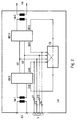
- FIG. 2 shows a block diagram of the conversion adapter UA.
- An essential part of this UA conversion adapter are two highly integrated circuits called IBCE and IBCV.
- the letter combination IBC stands for the English technical term: "ISDN burst transceiver circuit," which can be, for example, circuits with the type designation PEB 2095.
- the line side of one circuit IBCV is connected via a terminating transformer Ue2 to a plug which must be connected to the line side leading to a switching system VA.
- the other circuit IBCE is also connected with its line side via a transformer Ue1 to a plug-in device, where the end of the transmission line leading to a terminal EG is to be connected.
- the clocks generated by one of the circuits IBCV are offered to the other circuit IBCE and fed to a code recognizer CE.
- these clock lines RT and DT are routed via amplifier circuits V2 and V3 to the plug-in device S, where a data display device with a display device AE can be connected.
- the respective data outputs DAV and DAE of the highly integrated circuits IBCV and IBCE are connected to the code recognizer CE.
- the mentioned outputs DAV and DAE are routed to sockets of the plug device S via amplifier circuits V4 and V1.
- the output signals of the data outputs DAV and DAE are fed to a logic arrangement, which is shown in more detail in FIG.
- the outputs of this logic arrangement are connected to the data inputs DEV and DEE of the integrated circuits IBCV and IBCE. These connections are switched such that the signals coming from the data output DAV of the one integrated circuit IBCV are fed to the data input DEE of the other integrated circuit IBCE.
- the output signals of the data output DAE of the first circuit IBCE arrive at the data input DEV of the other integrated circuit IBCV. This crosswise connection is indicated by dashed lines in the drawing.
- This connection of the data outputs DAV and DAE with the respective other data inputs DEE and DEV ensures that the data exchange can continue to take place in the time separation method, as is used in the Upo interface.
- An external circuit (not shown) ensures that the two integrated circuits IBCV and IBCE operate in different operating modes.
- the so-called NT mode is set for the circuit IBCV, which is located on the side of the switching system VA.
- Another circuit of the second circuit IBCE which is located on the line side leading to a terminal EG, is set to a so-called LT mode.
- the two integrated circuits IBCV and IBCE are thus able to work together in the wiring as described above in such a way that the data exchange can take place both on the user data channels and on the signaling channel.
- the code recognizer CE has the task of recognizing at least one special command in the signaling channel. This special command is used when the integrated circuits IBCV and IBCE are used differently to set a special operating mode. This particular mode of operation would lead to the termination of a data transmission in the present application. Therefore, such a command is recognized by the code recognizer CE and modified in such a way that the aforementioned effect cannot occur.
- FIG. 3 A more detailed circuit diagram of this code recognizer CE is shown in FIG. 3. The function of this circuit arrangement is now described in more detail with reference to the time diagram shown in FIG. 4.
- the frame clock RT is linked to the data clock DT in a delay device VZ.
- This delay device VZ can consist of a multi-stage shift register, of which only one stage is shown for the sake of simplicity.
- the delay device VZ supplies a delay clock VT, which is fed to a count generator ZG.
- This count generator ZG is connected to the frame clock RT at its charging input L. With the appearance of the frame clock RT, the count generator ZG is therefore loaded to a predetermined binary value (for example 2).
- the count generator ZG is counted further with the delay clock VT, so that a bit comparison can take place at a predetermined binary value.
- a decoding DEC is provided which emits a pulse to the two comparators VG1 and VG2, so that they can carry out a bit comparison from this point in time.
- This measure precisely specifies the point in time at which the command to be recognized is located in the form of a bit combination within a data word.
- FIG. 4 shows that for a period of 4 bits (shown in broken lines) the curve of the signal at the output C of the count generator ZG corresponds to the curve of the signal at one of the data outputs DAE or DAV. If a match of the respectively received bit with the bit pattern of the code to be recognized is determined by one of the comparators VG1 or VG2, then the relevant code converter CW1 or CW2 receives a pulse. A counter located in the code converter CW1 or CW2 is thus counted one step further.
- the respective code converter CW1 or CW2 When a predetermined counting position is reached, the respective code converter CW1 or CW2 emits an output signal, whereby an AND gate UG1 or UG2 connected to it is blocked. This creates a logic zero signal at the output of the corresponding AND gate UG1 or UG2, which then reaches the relevant data input DEE or DEV.
- the decoding DEC by the comparators VG1 or VG2 If it is determined with the aid of the count generator ZG, the decoding DEC by the comparators VG1 or VG2, that 3 bits (011) match from the beginning of the period specified for the observation, the fourth bit is forcibly set to zero. This is done by the code converters CW1 and CW2 and has the consequence that the data inputs DEE and DEV of the integrated circuits IBCE and IBCV are offered a modified command structure. This prevents the integrated circuits IBCE or IBCV from entering a working mode which prevents further data transmission.
- the circuit arrangement of the code recognizer CE described here is designed for an application in the manner described. If the command to be eliminated consists of a different bit combination, the principle can be retained, but the logic arrangements and their wiring must be designed differently.
- the example described here, where the command consists of 4 bits, is not necessarily limited to this number of bits.
- command structures can also be recognized which consist of more than 4 bits.
- the time position of the command to be recognized by the code recognizer CE within the data stream must be known so that the time used for the code recognizer CE can be correctly determined.
- the conversion adapter UA can be connected to a data display device, i.e. be connected to a display device AE.
- a data display device i.e. be connected to a display device AE.
- the conversion adapter UA can also be operated without the connection of a display device and can be introduced into the Upo transmission link at a suitable point. With a suitable power supply either out The conversion adapter can then act as a regenerator or signal repeater in the network or via the connecting line, thus increasing the range of the transmission link.
Landscapes
- Engineering & Computer Science (AREA)
- Computer Networks & Wireless Communication (AREA)
- Data Exchanges In Wide-Area Networks (AREA)
- Communication Control (AREA)
Applications Claiming Priority (2)
| Application Number | Priority Date | Filing Date | Title |
|---|---|---|---|
| DE19924215945 DE4215945C1 (fr) | 1992-05-14 | 1992-05-14 | |
| DE4215945 | 1992-05-14 |
Publications (2)
| Publication Number | Publication Date |
|---|---|
| EP0573735A2 true EP0573735A2 (fr) | 1993-12-15 |
| EP0573735A3 EP0573735A3 (en) | 1997-08-13 |
Family
ID=6458874
Family Applications (1)
| Application Number | Title | Priority Date | Filing Date |
|---|---|---|---|
| EP93101921A Withdrawn EP0573735A3 (en) | 1992-05-14 | 1993-02-08 | Converting adapter for determining signalling data in an isdn upo-interface |
Country Status (2)
| Country | Link |
|---|---|
| EP (1) | EP0573735A3 (fr) |
| DE (1) | DE4215945C1 (fr) |
Cited By (7)
| Publication number | Priority date | Publication date | Assignee | Title |
|---|---|---|---|---|
| WO1995032575A3 (fr) * | 1994-05-17 | 1996-02-08 | British Telecomm | Installation terminale de reseau |
| NL1000238C2 (nl) * | 1995-04-27 | 1996-10-29 | Nederland Ptt | Werkwijze voor het monitoren van een via ten minste één telecommunicatielink te verzenden signaal, monitorsysteem monitorbesturingsinrichting en verwerkingsmiddelen. |
| WO1998024261A3 (fr) * | 1996-11-29 | 1998-10-01 | Tektronix Berlin Gmbh | Dispositif de mesure pour l'interface d'un chainon de voie de transmission avec une transmission en duplex integral dans un procede de duplex a porteuse commune |
| WO1999031925A1 (fr) * | 1997-12-15 | 1999-06-24 | Hewlett-Packard Company | Surveillance de liaisons rnis |
| EP1006750A1 (fr) * | 1998-12-04 | 2000-06-07 | Lucent Technologies Inc. | Interface à trois voies pour contrôle de signaux |
| EP1385352A1 (fr) * | 2002-07-24 | 2004-01-28 | Alcatel | Unité de surveillance d'une interface U RNIS |
| EP1432275A1 (fr) * | 2002-12-17 | 2004-06-23 | Alcatel | Appareil de surveillance |
Families Citing this family (1)
| Publication number | Priority date | Publication date | Assignee | Title |
|---|---|---|---|---|
| DE102004032875B4 (de) * | 2004-07-07 | 2014-07-10 | Deutsche Telekom Ag | Vorrichtung zum Überwachen wenigstens einer digitalen Anschlussleitung zur breitbandigen Datenübertragung |
Family Cites Families (3)
| Publication number | Priority date | Publication date | Assignee | Title |
|---|---|---|---|---|
| US4965795A (en) * | 1988-05-10 | 1990-10-23 | Harris Corporation | D channel monitor |
| JPH0421299A (ja) * | 1990-05-16 | 1992-01-24 | Fujitsu Ltd | Isdn―s点収容方式 |
| EP0475749B1 (fr) * | 1990-09-12 | 1996-04-24 | Nec Corporation | Terminal RNIS avec fonction de diagnostic |
-
1992
- 1992-05-14 DE DE19924215945 patent/DE4215945C1/de not_active Expired - Lifetime
-
1993
- 1993-02-08 EP EP93101921A patent/EP0573735A3/de not_active Withdrawn
Cited By (11)
| Publication number | Priority date | Publication date | Assignee | Title |
|---|---|---|---|---|
| WO1995032575A3 (fr) * | 1994-05-17 | 1996-02-08 | British Telecomm | Installation terminale de reseau |
| US5841836A (en) * | 1994-05-17 | 1998-11-24 | British Telecommunications Public Limited Company | Network termination equipment |
| NL1000238C2 (nl) * | 1995-04-27 | 1996-10-29 | Nederland Ptt | Werkwijze voor het monitoren van een via ten minste één telecommunicatielink te verzenden signaal, monitorsysteem monitorbesturingsinrichting en verwerkingsmiddelen. |
| WO1996034506A1 (fr) * | 1995-04-27 | 1996-10-31 | Koninklijke Ptt Nederland N.V. | Procede et systeme de controle |
| US5708713A (en) * | 1995-04-27 | 1998-01-13 | Koninklijke Ptt Nederland N.V. | Method for monitoring a signal to be transmitted via at least one telecommunication link, a monitoring system, a monitor controlling device and processing means |
| AU707305B2 (en) * | 1995-04-27 | 1999-07-08 | Koninklijke Kpn N.V. | Monitoring method and monitoring system |
| WO1998024261A3 (fr) * | 1996-11-29 | 1998-10-01 | Tektronix Berlin Gmbh | Dispositif de mesure pour l'interface d'un chainon de voie de transmission avec une transmission en duplex integral dans un procede de duplex a porteuse commune |
| WO1999031925A1 (fr) * | 1997-12-15 | 1999-06-24 | Hewlett-Packard Company | Surveillance de liaisons rnis |
| EP1006750A1 (fr) * | 1998-12-04 | 2000-06-07 | Lucent Technologies Inc. | Interface à trois voies pour contrôle de signaux |
| EP1385352A1 (fr) * | 2002-07-24 | 2004-01-28 | Alcatel | Unité de surveillance d'une interface U RNIS |
| EP1432275A1 (fr) * | 2002-12-17 | 2004-06-23 | Alcatel | Appareil de surveillance |
Also Published As
| Publication number | Publication date |
|---|---|
| EP0573735A3 (en) | 1997-08-13 |
| DE4215945C1 (fr) | 1993-05-06 |
Similar Documents
| Publication | Publication Date | Title |
|---|---|---|
| EP0213063A1 (fr) | Circuit pour tester un système de bus passif (méthode d'accès CSMA/CD) | |
| DE3416990C2 (de) | Prüfsystem bei einer Signalübermittlungsanlage | |
| CH661629A5 (de) | Verfahren und schaltungsanordnung zur fehlerortung bei einem digitalen fernmelde-teilnehmeranschluss. | |
| DE2838757A1 (de) | Schnittstellenschaltung fuer zeitmultiplexleitungen von nachrichtenvermittlungsanlagen | |
| EP0689747A1 (fr) | Reconnaissance de debit binaire | |
| DE3225773C2 (fr) | ||
| DE4215945C1 (fr) | ||
| DE3311386C2 (de) | Verfahren zum Betreiben von Endgeräten eines digitalen Teilnehmeranschlusses | |
| DE2700144B2 (de) | Datenübertragungssystem | |
| EP0106985B1 (fr) | Surveillance d'exploitation de voies de transmission numériques | |
| DE68919437T2 (de) | Schaltungsanordnung zur Detektion von Kodeverletzungen in AMI-Signalübertragung. | |
| DE3921411A1 (de) | Verfahren und vorrichtung zur uebermittlung binaerer nachrichten ueber einen seriellen nachrichtenbus | |
| DE3806262C1 (en) | Circuit arrangement for monitoring the state of switching points in a digital space-division switching network | |
| EP0468234B1 (fr) | Procédé pour l'élévation de la sécurité de perturbation dans un système de signalisation de risque | |
| DE2521731C2 (de) | Verfahren und Anordnung zur sendeseitigen asynchronen Übernahme, Übertragung und empfangsseitigen Übergabe digitaler Signale | |
| DE4139265C2 (de) | Telekommunikations-Datenzugriffsgerät | |
| EP0435873B1 (fr) | Procede de mesure dans le domaine utilisateurs d'un reseau numerique a integration de services (isdn) | |
| DE9317946U1 (de) | Schnittstellenkabel für Datenendeinrichtungen und Prüfeinrichtung | |
| DE3739481C2 (fr) | ||
| DE2945032C2 (de) | Verfahren zur Prüfung der Sendeeinrichtung für Wahlinformationen von Verbindungsleitungs- Übertragungen | |
| DE3015827C2 (de) | Übertragungssystem für digitale Signale mit einer Einrichtung zur Fehlerortung | |
| DE19826388A1 (de) | Fehlerverarbeitungsschaltung für eine Empfangsstelle eines Datenübertragungssystems | |
| DE3726573C2 (fr) | ||
| DE2753364A1 (de) | Signalempfaenger zur erkennung und auswertung von analogen signalen | |
| DE1952549C3 (de) | Schaltungsanordnung zur Übertragung von Impulsen |
Legal Events
| Date | Code | Title | Description |
|---|---|---|---|
| PUAI | Public reference made under article 153(3) epc to a published international application that has entered the european phase |
Free format text: ORIGINAL CODE: 0009012 |
|
| AK | Designated contracting states |
Kind code of ref document: A2 Designated state(s): AT BE ES FR GB IT NL |
|
| RAP3 | Party data changed (applicant data changed or rights of an application transferred) |
Owner name: TELENORMA GMBH |
|
| RAP1 | Party data changed (applicant data changed or rights of an application transferred) |
Owner name: ROBERT BOSCH GMBH |
|
| PUAL | Search report despatched |
Free format text: ORIGINAL CODE: 0009013 |
|
| AK | Designated contracting states |
Kind code of ref document: A3 Designated state(s): AT BE ES FR GB IT NL |
|
| STAA | Information on the status of an ep patent application or granted ep patent |
Free format text: STATUS: THE APPLICATION IS DEEMED TO BE WITHDRAWN |
|
| 18D | Application deemed to be withdrawn |
Effective date: 19980214 |
|
| RIN1 | Information on inventor provided before grant (corrected) |
Inventor name: VANEGAS-DORN, JESUS ERNESTO Inventor name: FREISLEBEN, WALTER |