EP0573838A2 - Mehrchipmodul - Google Patents
Mehrchipmodul Download PDFInfo
- Publication number
- EP0573838A2 EP0573838A2 EP93108381A EP93108381A EP0573838A2 EP 0573838 A2 EP0573838 A2 EP 0573838A2 EP 93108381 A EP93108381 A EP 93108381A EP 93108381 A EP93108381 A EP 93108381A EP 0573838 A2 EP0573838 A2 EP 0573838A2
- Authority
- EP
- European Patent Office
- Prior art keywords
- carrier
- capacitor
- conductive layer
- enlarged
- chip module
- Prior art date
- Legal status (The legal status is an assumption and is not a legal conclusion. Google has not performed a legal analysis and makes no representation as to the accuracy of the status listed.)
- Granted
Links
Images

Classifications
-
- H—ELECTRICITY
- H10—SEMICONDUCTOR DEVICES; ELECTRIC SOLID-STATE DEVICES NOT OTHERWISE PROVIDED FOR
- H10W—GENERIC PACKAGES, INTERCONNECTIONS, CONNECTORS OR OTHER CONSTRUCTIONAL DETAILS OF DEVICES COVERED BY CLASS H10
- H10W90/00—Package configurations
-
- H—ELECTRICITY
- H10—SEMICONDUCTOR DEVICES; ELECTRIC SOLID-STATE DEVICES NOT OTHERWISE PROVIDED FOR
- H10W—GENERIC PACKAGES, INTERCONNECTIONS, CONNECTORS OR OTHER CONSTRUCTIONAL DETAILS OF DEVICES COVERED BY CLASS H10
- H10W20/00—Interconnections in chips, wafers or substrates
- H10W20/40—Interconnections external to wafers or substrates, e.g. back-end-of-line [BEOL] metallisations or vias connecting to gate electrodes
- H10W20/495—Capacitive arrangements or effects of, or between wiring layers
- H10W20/496—Capacitor integral with wiring layers
-
- H—ELECTRICITY
- H10—SEMICONDUCTOR DEVICES; ELECTRIC SOLID-STATE DEVICES NOT OTHERWISE PROVIDED FOR
- H10W—GENERIC PACKAGES, INTERCONNECTIONS, CONNECTORS OR OTHER CONSTRUCTIONAL DETAILS OF DEVICES COVERED BY CLASS H10
- H10W44/00—Electrical arrangements for controlling or matching impedance
- H10W44/601—Capacitive arrangements
-
- H—ELECTRICITY
- H10—SEMICONDUCTOR DEVICES; ELECTRIC SOLID-STATE DEVICES NOT OTHERWISE PROVIDED FOR
- H10W—GENERIC PACKAGES, INTERCONNECTIONS, CONNECTORS OR OTHER CONSTRUCTIONAL DETAILS OF DEVICES COVERED BY CLASS H10
- H10W70/00—Package substrates; Interposers; Redistribution layers [RDL]
- H10W70/20—Conductive package substrates serving as an interconnection, e.g. metal plates
- H10W70/24—Conductive package substrates serving as an interconnection, e.g. metal plates characterised by materials
- H10W70/26—Semiconductor materials
-
- H—ELECTRICITY
- H10—SEMICONDUCTOR DEVICES; ELECTRIC SOLID-STATE DEVICES NOT OTHERWISE PROVIDED FOR
- H10W—GENERIC PACKAGES, INTERCONNECTIONS, CONNECTORS OR OTHER CONSTRUCTIONAL DETAILS OF DEVICES COVERED BY CLASS H10
- H10W70/00—Package substrates; Interposers; Redistribution layers [RDL]
- H10W70/60—Insulating or insulated package substrates; Interposers; Redistribution layers
- H10W70/67—Insulating or insulated package substrates; Interposers; Redistribution layers characterised by their insulating layers or insulating parts
- H10W70/69—Insulating materials thereof
- H10W70/698—Semiconductor materials that are electrically insulating, e.g. undoped silicon
-
- H—ELECTRICITY
- H10—SEMICONDUCTOR DEVICES; ELECTRIC SOLID-STATE DEVICES NOT OTHERWISE PROVIDED FOR
- H10W—GENERIC PACKAGES, INTERCONNECTIONS, CONNECTORS OR OTHER CONSTRUCTIONAL DETAILS OF DEVICES COVERED BY CLASS H10
- H10W90/00—Package configurations
- H10W90/701—Package configurations characterised by the relative positions of pads or connectors relative to package parts
- H10W90/751—Package configurations characterised by the relative positions of pads or connectors relative to package parts of bond wires
- H10W90/754—Package configurations characterised by the relative positions of pads or connectors relative to package parts of bond wires between a chip and a stacked insulating package substrate, interposer or RDL
Definitions
- the invention relates to a multi-chip module.
- This is an arrangement with electronic components, such as is increasingly used for the space and cost-saving construction of highly integrated electronic components.
- electronic components in particular digital and analog integrated circuits, which are partially implemented on different substrates such as silicon or gallium arsenide, are arranged on a carrier together with passive components.
- the electronic components are firmly connected to the carrier and are electrically connected to one another in accordance with the intended application.
- silicon or ceramic carriers are used as carriers.
- capacitors with capacities in the range from nF to 10 ⁇ F are required. Capacitors in this capacitance range cannot be integrated in the integrated circuits.
- the capacitor components are mostly used in SMD design. This solution is costly and space-consuming and also means that the capacitors cannot be placed anywhere close to the integrated circuits. Furthermore, the discrete capacitor components have a considerably greater overall height than the integrated circuits and therefore limit the minimum overall height of the arrangement.
- the invention is based on the problem of specifying a multi-chip module which comprises a capacitor of large specific capacitance and which can nevertheless be implemented in a reduced overall height.
- the arrangement comprises a capacitor which is realized on a monocrystalline silicon substrate, the surface of which is enlarged at least in the region of the capacitor by electrochemical etching in a fluoride-containing, acidic electrolyte in which the silicon substrate is connected as an anode.
- the surface of the silicon substrate is structured in a characteristic manner by the electrochemical etching. Holes are formed which are arranged more or less regularly depending on the pretreatment of the substrate and which have a high aspect ratio up to the range of approximately 1: 400.
- Capacitors of high specific capacitance can be realized on such a surface by depositing a dielectric layer and a conductive layer as counterelectrode.
- Such silicon-based capacitors typically have specific capacities of 10 ⁇ FV / mm3.
- a capacitor with 10 ⁇ F and 10V nominal voltage can therefore be realized on an area of approximately 10 mm2 with an aspect ratio of 1: 400.
- the carrier consists of monocrystalline silicon.
- the surface of the carrier is at least partially by electrochemical etching in a fluoride-containing, acidic electrolyte, in which the carrier acts as an anode is connected, enlarged.
- the capacitor is implemented in the carrier in the area of the enlarged surface. It is within the scope of the invention to define the size of the capacitor by the geometry of the conductive layer. This makes it possible to arrange other electronic components at least partially above the capacitor. This enables a space-saving arrangement.
- part of the surface of the carrier is not enlarged and that connections for contacting the chips are arranged in this part of the surface of the carrier. This results in a lateral separation of connections and capacitors.
- the capacitor and the integrated circuit it is within the scope of the invention to provide a metallization on the surface of the carrier.
- the substrate with the integrated circuit is arranged on the surface of the carrier such that it at least partially overlaps the metallization. In this way, a low-resistance electrical connection between the individual electronic components is possible. Such an arrangement can be produced by flip-chip assembly.
- a capacitor is explained with reference to FIG. 1, which is implemented on a monocrystalline silicon substrate, the surface of which is enlarged at least in the region of the capacitor by electrochemical etching in an acidic electrolyte containing fluoride, in which the silicon substrate is connected as an anode.
- the hole openings 13 have a diameter of, for example, 3 ⁇ m and a depth of, for example, 200 ⁇ m.
- the hole openings 13 are formed with the aid of an electrochemical etching. For example, 6 percent hydrofluoric acid (HF) is used as the electrolyte.
- HF hydrofluoric acid
- the n-doped substrate is acted on as a anode with a potential of 3 volts.
- the substrate is illuminated from the back.
- a current density of, for example, 10 milliamperes / cm2 is set.
- the surface 12 is in contact with the electrolyte. After approximately 150 minutes of etching time, the hole openings 13 have a depth of 200 ⁇ m.
- the surface of the hole openings 13 and the surface 12 remaining therebetween is conformally covered with a dielectric layer 14.
- the dielectric layer 14 consists, for example, of SiO2 and has a thickness of, for example, 92 nm.
- a conductive layer 15 is arranged on the dielectric layer 14.
- the conductive layer 15 consists, for example, of n-doped polysilicon.
- the conductive layer 15 completely covers the dielectric layer 14.
- the conductive layer 15 is contacted by a first contact 16.
- the first contact 16 is made of aluminum, for example. Due to the surface tension of the aluminum, the first contact 16 consists of a continuous layer which only contacts the upper part of the conductive layer 15 in the region of the hole openings 13.
- the conductive layer 15 and the substrate 11 act as capacitor electrodes in the capacitor.
- a second contact 17 made of, for example, aluminum is applied to a surface of the substrate facing away from surface 12.
- a carrier 21 made of monocrystalline silicon has a region 22 in the surface in which the surface is enlarged by an electrochemical etching in a fluoride-containing, acidic electrolyte, in which the carrier is connected as an anode.
- Capacitors 23 are realized in this area 22.
- the size of the capacitors 23 is defined by the geometry of a conductive layer that acts as a capacitor electrode. Outside the area 22, electronic components z.
- B. integrated circuits 24 arranged in substrates.
- Metallizations 25 are arranged on the surface of the capacitors 23 and extend to the surface of the carrier 21. As a result, the metallizations 25 simultaneously form a contact with the conductive layer of the respective capacitors 23 and represent a connection option for integrated circuits. This connection is realized for example via bond wires 26.
- the electrical connection between the metallization 25 and an integrated circuit 24 can also be realized in that the integrated circuit 24 is arranged partially above the metallization 25. In this case, the contact is made via the back of the substrate in which the integrated circuit 24 is integrated.
- Such an electrical connection can be implemented, for example, by flip-chip assembly.
- a carrier 31 made of monocrystalline silicon is used, the surface of which is provided with a perforated structure by anodic, electrochemical etching in a fluoride-containing, acidic electrolyte and is thereby enlarged.
- Capacitors 32 are implemented in the surface, the size of which is determined by the geometry of the conductive layer.
- a circuit 33 integrated in a substrate, for example, is arranged on the carrier 31 as an electronic component. It completely or partially overlaps the capacitors.
- An electrical connection between the integrated circuit 33 and the capacitors 32 is implemented via a metallization 34 on the surface of the carrier 31, which contacts the substrate containing the integrated circuit 33 from the rear. This embodiment allows a very space-saving arrangement of capacitors and integrated circuits.
Landscapes
- Semiconductor Integrated Circuits (AREA)
Abstract
Description
- Die Erfindung betrifft ein Multi-Chip-Modul. Das ist eine Anordnung mit elektronischen Komponenten, wie sie zum platz- und kostensparenden Aufbau von hochintegrierten elektronischen Komponenten zunehmend Anwendung findet. In einer solchen Anordnung werden unterschiedliche elektronische Komponenten, insbesondere digitale und analoge integrierte Schaltkreise, die teilweise auf unterschiedlichen Substraten wie Silizium oder Galliumarsenid realisiert sind, zusammen mit passiven Bauelementen auf einem Träger angeordnet. Die elektronischen Komponenten sind fest mit dem Träger verbunden und entsprechend der vorgesehenen Anwendung untereinander elektrisch verbunden. Als Träger werden zum Beispiel Silizium- oder Keramikträger verwendet.
- Für analoge integrierte Schaltungen und zur Entkopplung von digitalen integrierten Schaltungen von Störungen auf Versorgungsleitungen werden Kondensatoren mit Kapazitäten im Bereich von einem nF bis 10 µF benötigt. Kondensatoren in diesem Kapazitätsbereich lassen sich nicht in den integrierten Schaltungen integrieren.
- Deshalb werden sie in bekannten Multi-Chip-Modul-Konzepten als diskrete Kondensatorbauelemente auf dem Träger angeordnet. Die Kondensatorbauelemente werden dabei meist in SMD-Bauform verwendet. Diese Lösung ist kosten- und platzaufwendig und führt außerdem dazu, daß die Kondensatoren nicht beliebig nah an die integrierten Schaltungen plaziert werden können. Ferner weisen die diskreten Kondensatorbauelemente eine erheblich größere Bauhöhe auf als die integrierten Schaltungen und begrenzen daher die minimale Bauhöhe der Anordnung.
- Der Erfindung liegt das Problem zugrunde, ein Multi-Chip-Modul anzugeben, das einen Kondensator großer spezifischer Kapazität umfaßt und das dennoch in verminderter Bauhöhe realisierbar ist.
- Dieses Problem wird erfindungsgemäß gelöst durch eine Anordnung nach Anspruch 1.
- Die Anordnung umfaßt erfindungsgemäß einen Kondensator, der auf einem monokristallinen Siliziumsubstrat realisiert ist, dessen Oberfläche mindestens im Bereich des Kondensators durch eine elektrochemische Ätzung in einem fluoridhaltigen, sauren Elektrolyten, in dem das Siliziumsubstrat als Anode verschaltet ist, vergrößert ist. Durch die elektrochemische Ätzung wird die Oberfläche des Siliziumsubstrats auf charakteristische Weise strukturiert. Es entstehen Löcher, die je nach Vorbehandlung des Substrats mehr oder weniger regelmäßig angeordnet sind und die ein hohes Aspektverhältnis bis in den Bereich von etwa 1:400 aufweisen. Auf einer solchen Oberfläche sind durch Abscheidung einer dielektrischen Schicht und einer leitfähigen Schicht als Gegenelektrode Kondensatoren hoher spezifischer Kapazität realisierbar. Solche Kondensatoren auf Siliziumbasis haben typischerweise spezifische Kapazitäten von 10 µFV/mm³. Ein Kondensator mit 10 µF und 10V Nennspannung ist daher auf einer Fläche von etwa 10 mm² bei einem Aspektverhältnis von 1:400 realisierbar.
- Erfindungsgemäß besteht der Träger aus monokristallinem Silizium. Dabei ist die Oberfläche des Trägers mindestens teilweise durch elektrochemisches Ätzen in einem fluoridhaltigen, sauren Elektrolyten, in dem der Träger als Anode verschaltet ist, vergrößert. Der Kondensator ist in dem Träger im Bereich der vergrößerten Oberfläche realisiert. Es liegt im Rahmen der Erfindung, die Größe des Kondensators dabei durch die Geometrie der leitfähigen Schicht zu definieren. Dadurch ist es möglich, andere elektronische Komponenten mindestens teilweise oberhalb des Kondensators anzuordnen. Dadurch wird eine platzsparende Anordnung ermöglicht.
- Es liegt dabei im Rahmen der Erfindung, daß ein Teil der Oberfläche des Trägers nicht vergrößert ist und daß in diesem Teil der Oberfläche des Trägers Anschlüsse zur Kontaktierung der Chips angeordnet sind. Dadurch wird eine laterale Trennung von Anschlüssen und Kondensatoren erreicht.
- Zur elektrischen Verbindung des Kondensators und der integrierten Schaltung liegt es im Rahmen der Erfindung, an der Oberfläche des Trägers eine Metallisierung vorzusehen. Das Substrat mit der integrierten Schaltung wird so an der Oberfläche des Trägers angeordnet, daß es die Metallisierung mindestens teilweise überlappt. Auf diese Weise ist eine niederohmige elektrische Verbindung zwischen den einzelnen elektronischen Komponenten möglich. Eine solche Anordnung läßt sich durch Flip-Chip-Montage herstellen.
- Im folgenden wird die Erfindung anhand der Figuren und der Ausführungsbeispiele näher erläutert.
- Figur 1
- zeigt einen Kondensator, der auf einem monokristallinen Siliziumsubstrat realisiert ist, dessen Oberfläche durch anodisches elektrochemisches Ätzen in einem fluoridhaltigen, sauren Elektrolyten vergrößert ist.
- Figur 2
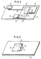
- zeigt eine Anordnung mit elektronischen Komponenten, die einen Träger aus monokristallinem Silizium umfaßt, dessen Oberfläche teilweise durch anodische, elektrochemische Ätzung vergrößert ist.
- Figur 3
- zeigt eine Anordnung mit elektronischen Komponenten mit einem Träger aus monokristallinem Silizium, dessen Oberfläche durchgehend durch anodische, elektrochemische Ätzung vergrößert ist und in dessen Oberfläche mindestens ein Kondensator realisiert ist.
- Anhand von Figur 1 wird ein Kondensator erläutert, der auf einem monokristallinen Siliziumsubstrat realisiert ist, dessen Oberfläche mindestens im Bereich des Kondensators durch elektrochemische Ätzungen in einem flouridhaltigen, sauren Elektrolyten, in dem das Siliziumsubstrat als Anode verschaltet ist, vergrößert ist.
- Ein Substrat 11 aus n-dotiertem, monokristallinem Silizium, das einen spezifischen Widerstand von zum Beispiel 5 Ohm . cm aufweist, ist an einer Oberfläche 12 mit einer Vielzahl von Lochöffnungen 13 versehen. Die Lochöffnungen 13 weisen einen Durchmesser von zum Beispiel 3 µm und eine Tiefe von zum Beispiel 200 µm auf. Die Lochöffnungen 13 sind mit Hilfe einer elektrochemischen Ätzung gebildet. Als Elektrolyt wird dabei zum Beispiel 6 prozentige Flußsäure (HF) verwendet. Das n-dotierte Substrat wird als Anode mit einem Potential von 3 Volt beaufschlagt. Das Substrat wird von der Rückseite her beleuchtet. Es wird eine Stromdichte von zum Beispiel 10 Milliampere/cm² eingestellt. Bei der elektrochemischen Ätzung ist die Oberfläche 12 mit dem Elektrolyten in Kontakt. Nach ungefähr 150 Minuten Ätzzeit weisen die Lochöffnungen 13 eine Tiefe von 200 µm auf.
- Die Oberfläche der Lochöffnungen 13 und der dazwischen verbleibenden Oberfläche 12 ist konform mit einer dielektrischen Schicht 14 bedeckt. Die dielektrische Schicht 14 besteht zum Beispiel aus SiO₂ und weist eine Dicke von zum Beispiel 92 nm auf. Auf der dielektrischen Schicht 14 ist eine leitfähige Schicht 15 angeordnet. Die leitfähige Schicht 15 besteht zum Beispiel aus n-dotiertem Polysilizium. Die leitfähige Schicht 15 bedeckt die dielektrische Schicht 14 vollständig. Die leitfähige Schicht 15 wird durch einen ersten Kontakt 16 kontaktiert. Der erste Kontakt 16 besteht zum Beispiel aus Aluminium. Aufgrund der Oberflächenspannung des Aluminiums besteht der erste Kontakt 16 aus einer durchgehenden Schicht, die im Bereich der Lochöffnungen 13 nur den oberen Teil der leitfähigen Schicht 15 kontaktiert. Die leitfähige Schicht 15 und das Substrat 11 wirken in dem Kondensator als Kondensatorelektroden. Auf einer der Oberfläche 12 abgewandten Oberfläche des Substrats ist ein zweiter Kontakt 17 aus zum Beispiel Aluminium aufgebracht.
- Ein Träger 21 aus monokristallinem Silizium (s. Figur 2) weist einen Bereich 22 in der Oberfläche auf, in der die Oberfläche durch eine elektrochemische Ätzung in einem fluoridhaltigen, sauren Elektrolyten, in dem der Träger als Anode verschaltet ist, vergrößert ist. In diesem Bereich 22 sind Kondensatoren 23 realisiert. Die Größe der Kondensatoren 23 ist dabei durch die Geometrie einer leitfähigen Schicht, die als Kondensatorelektrode wirkt, definiert. Außerhalb des Bereichs 22 sind auf dem Träger 21 elektronische Komponenten z. B. in Substrate integrierte Schaltungen 24 angeordnet. Metallisierungen 25 sind an der Oberfläche der Kondensatoren 23 angeordnet und erstrecken sich auf die Oberfläche des Trägers 21. Dadurch bilden die Metallisierungen 25 gleichzeitig einen Kontakt zu der leitfähigen Schicht des jeweiligen Kondensators 23 und stellen eine Anschlußmöglichkeit für integrierte Schaltungen dar. Dieser Anschluß wird zum Beispiel über Bonddrähte 26 realisiert.
- Die elektrische Verbindung zwischen der Metallisierung 25 und einer integrierten Schaltung 24 kann auch dadurch realisiert werden, daß die integrierte Schaltung 24 teilweise oberhalb der Metallisierung 25 angeordnet ist. Der Kontakt erfolgt in diesem Fall über die Rückseite des Substrats, in dem die integrierte Schaltung 24 integriert ist. Eine solche elektrische Verbindung kann zum Beispiel durch Flip-Chip-Montage realisiert werden.
- In einem anderen Ausführungsbeispiel (siehe Figur 3) wird ein Träger 31 aus monokristallinem Silizium verwendet, dessen Oberfläche durch eine anodische, elektrochemische Ätzung in einem fluoridhaltigen, sauren Elektrolyten mit einer Lochstruktur versehen und dadurch vergrößert ist. In der Oberfläche sind Kondensatoren 32 realisiert, deren Größe durch die Geometrie der leitfähigen Schicht festgelegt ist. Auf dem Träger 31 ist als elektronische Komponente zum Beispiel eine in einem Substrat integrierte Schaltung 33 angeordnet. Sie überlappt die Kondensatoren ganz oder teilweise. Eine elektrische Verbindung zwischen der integrierten Schaltung 33 und den Kondensatoren 32 ist über eine Metallisierung 34 an der Oberfläche des Trägers 31, die das die integrierte Schaltung 33 enthaltende Substrat von der Rückseite her kontaktiert, realisiert. Diese Ausführungsform erlaubt eine sehr platzsparende Anordnung von Kondensatoren und integrierten Schaltungen.
Claims (5)
- Multi-Chip-Modul,- bei dem ein Träger (21, 31) aus monokristallinem Silizium vorgesehen ist, dessen Oberfläche mindestens teilweise durch elektrochemische Ätzung in einem fluoridhaltigen, sauren Elektrolyten, in dem der Träger als Anode verschaltet ist, vergrößert ist,- bei dem auf der vergrößerten Oberfläche mindestens ein Kondensator angeordnet ist, der eine dielektrische Schicht, die auf der vergrößerten Oberfläche angeordnet ist, und eine leitfähige Schicht, die auf der dielektrischen Schicht angeordnet ist, umfaßt, wobei der Träger und die leitfähige Schicht als Kondensatorelektroden wirken.
- Multi-Chip-Modul nach Anspruch 1,
bei dem die Größe des Kondensators durch die Geometrie der leitfähigen Schicht definiert ist. - Multi-Chip-Modul nach Anspruch 1 oder 2,
bei dem ein Teil der Oberfläche des Trägers nicht vergrößert ist und in diesem Teil der Oberfläche des Trägers Anschlüsse zur Kontaktierung der Chips angeordnet sind. - Multi-Chip-Modul nach einem der Ansprüche 1 bis 3,- bei dem zur elektrischen Verbindung von Kondensator (23, 32) und anderen elektronischen Komponenten (24, 33) an der Oberfläche des Trägers (21, 31) eine Metallisierung (25, 34) angeordnet ist und- bei der mindestens ein Substrat mit einer elektronischen Komponente (24, 33) so an der Oberfläche des Trägers (21, 31) angeordnet ist, daß es die Metallisierung (25, 34) mindestens teilweise überlappt.
- Anordnung nach Anspruch 4,
bei der mindestens eine elektronische Komponente mindestens teilweise oberhalb des Kondensators (32) angeordnet ist.
Applications Claiming Priority (2)
| Application Number | Priority Date | Filing Date | Title |
|---|---|---|---|
| DE4219031 | 1992-06-10 | ||
| DE4219031A DE4219031C2 (de) | 1992-06-10 | 1992-06-10 | Multi-Chip-Modul mit Kondensator, der auf dem Träger aus Silizium (monokristalines Substrat) realisiert ist |
Publications (3)
| Publication Number | Publication Date |
|---|---|
| EP0573838A2 true EP0573838A2 (de) | 1993-12-15 |
| EP0573838A3 EP0573838A3 (de) | 1994-08-31 |
| EP0573838B1 EP0573838B1 (de) | 1997-03-05 |
Family
ID=6460735
Family Applications (1)
| Application Number | Title | Priority Date | Filing Date |
|---|---|---|---|
| EP93108381A Expired - Lifetime EP0573838B1 (de) | 1992-06-10 | 1993-05-24 | Mehrchipmodul |
Country Status (4)
| Country | Link |
|---|---|
| US (1) | US5365405A (de) |
| EP (1) | EP0573838B1 (de) |
| JP (1) | JPH0669416A (de) |
| DE (2) | DE4219031C2 (de) |
Cited By (2)
| Publication number | Priority date | Publication date | Assignee | Title |
|---|---|---|---|---|
| EP0692799A3 (de) * | 1994-07-15 | 1997-05-14 | Plessey Semiconductors Ltd | Trimmbarer Kondensator |
| DE19708970A1 (de) * | 1997-03-05 | 1998-10-01 | Reinz Dichtungs Gmbh | Metallische Flachdichtung |
Families Citing this family (14)
| Publication number | Priority date | Publication date | Assignee | Title |
|---|---|---|---|---|
| EP0645621A3 (de) * | 1993-09-28 | 1995-11-08 | Siemens Ag | Sensoranordnung. |
| DE4429289A1 (de) * | 1994-08-18 | 1996-02-22 | Telefunken Microelectron | Integrierte Schaltungsanordnung |
| US5534465A (en) * | 1995-01-10 | 1996-07-09 | At&T Corp. | Method for making multichip circuits using active semiconductor substrates |
| US6462976B1 (en) | 1997-02-21 | 2002-10-08 | University Of Arkansas | Conversion of electrical energy from one form to another, and its management through multichip module structures |
| US7144486B1 (en) | 1997-04-30 | 2006-12-05 | Board Of Trustees Of The University Of Arkansas | Multilayer microcavity devices and methods |
| US7169272B2 (en) * | 1997-04-30 | 2007-01-30 | Board Of Trustees Of The University Of Arkansas | Microfabricated recessed disk microelectrodes: characterization in static and convective solutions |
| DE19928733A1 (de) * | 1999-06-23 | 2001-01-04 | Giesecke & Devrient Gmbh | Halbleiterspeicher-Chipmodul |
| DE19943251A1 (de) * | 1999-09-10 | 2001-04-05 | Bosch Gmbh Robert | Kondensatorbauelement |
| US7348183B2 (en) * | 2000-10-16 | 2008-03-25 | Board Of Trustees Of The University Of Arkansas | Self-contained microelectrochemical bioassay platforms and methods |
| US6887714B2 (en) | 2000-10-16 | 2005-05-03 | Board Of Trustees Of The University Of Arkansas, N.A. | Microvolume immunoabsorbant assays with amplified electrochemical detection |
| US7456028B2 (en) | 2000-10-16 | 2008-11-25 | Board Of Trustees Of The University Of Arkansas, N.A. | Electrochemical method for detecting water born pathogens |
| JP2002299462A (ja) * | 2001-01-26 | 2002-10-11 | Nokia Mobile Phones Ltd | 半導体装置 |
| JP2003282721A (ja) | 2002-03-26 | 2003-10-03 | Murata Mfg Co Ltd | 半導体装置および送受信装置 |
| DE102008035993B4 (de) * | 2008-08-01 | 2018-10-11 | Infineon Technologies Ag | Leistungshalbleitermodul |
Family Cites Families (7)
| Publication number | Priority date | Publication date | Assignee | Title |
|---|---|---|---|---|
| US3962713A (en) * | 1972-06-02 | 1976-06-08 | Texas Instruments Incorporated | Large value capacitor |
| US4153988A (en) * | 1977-07-15 | 1979-05-15 | International Business Machines Corporation | High performance integrated circuit semiconductor package and method of making |
| JP2520419B2 (ja) * | 1987-04-17 | 1996-07-31 | 日本電気株式会社 | 資源アクセス方式 |
| EP0296348B1 (de) * | 1987-05-27 | 1993-03-31 | Siemens Aktiengesellschaft | Ätzverfahren zum Erzeugen von Lochöffnungen oder Gräben in n-dotiertem Silizium |
| JPH01251778A (ja) * | 1988-03-31 | 1989-10-06 | Toshiba Corp | Icカード |
| JPH0635462Y2 (ja) * | 1988-08-11 | 1994-09-14 | 株式会社村田製作所 | 積層型コンデンサ |
| RU2082258C1 (ru) * | 1991-08-14 | 1997-06-20 | Сименс АГ | Схемная структура с по меньшей мере одним конденсатором и способ ее изготовления |
-
1992
- 1992-06-10 DE DE4219031A patent/DE4219031C2/de not_active Expired - Fee Related
-
1993
- 1993-05-21 US US08/064,235 patent/US5365405A/en not_active Expired - Fee Related
- 1993-05-24 EP EP93108381A patent/EP0573838B1/de not_active Expired - Lifetime
- 1993-05-24 DE DE59305563T patent/DE59305563D1/de not_active Expired - Fee Related
- 1993-06-04 JP JP5160302A patent/JPH0669416A/ja active Pending
Cited By (3)
| Publication number | Priority date | Publication date | Assignee | Title |
|---|---|---|---|---|
| EP0692799A3 (de) * | 1994-07-15 | 1997-05-14 | Plessey Semiconductors Ltd | Trimmbarer Kondensator |
| DE19708970A1 (de) * | 1997-03-05 | 1998-10-01 | Reinz Dichtungs Gmbh | Metallische Flachdichtung |
| DE19708970B4 (de) * | 1997-03-05 | 2009-09-24 | Reinz-Dichtungs-Gmbh | Metallische Flachdichtung |
Also Published As
| Publication number | Publication date |
|---|---|
| EP0573838B1 (de) | 1997-03-05 |
| US5365405A (en) | 1994-11-15 |
| DE4219031C2 (de) | 1994-11-10 |
| DE4219031A1 (de) | 1993-12-16 |
| JPH0669416A (ja) | 1994-03-11 |
| EP0573838A3 (de) | 1994-08-31 |
| DE59305563D1 (de) | 1997-04-10 |
Similar Documents
| Publication | Publication Date | Title |
|---|---|---|
| DE2542518C3 (de) | ||
| EP0573838B1 (de) | Mehrchipmodul | |
| DE1298630C2 (de) | Integrierte schaltungsanordnung | |
| DE68920944T2 (de) | Packungsstrukturen für integrierte Mehrschichtschaltungen. | |
| DE68916784T2 (de) | Integrierte Schaltungspackung. | |
| EP0035093B1 (de) | Anordnung zum Packen mehrerer schnellschaltender Halbleiterchips | |
| EP0000384B1 (de) | Anordnung zum Packen schnell schaltender monolitisch integrierter Halbleiterschaltungen, die für die Anschlusspunkte der Stromversorgung des Halbleiterplättchens Entkoppelkondensatoren aufweist, und ein Verfahren zur Herstellung der Anordnung. | |
| DE10019838B4 (de) | Mehrschichtkondensator, Verdrahtungssubstrat damit und Verwendung eines derartigen Mehrschichtkondensators | |
| DE19755954B4 (de) | Leiterrahmenstruktur, diese verwendende Halbleiterbaugruppe und Herstellungsverfahren hierfür | |
| EP0351581A1 (de) | Hochintegrierte Schaltung sowie Verfahren zu deren Herstellung | |
| DE404295T1 (de) | Kondensatoren fuer integrierte schaltungen. | |
| DE4325668A1 (de) | Mehrebenen-Verdrahtungssubstrat und dieses verwendende Halbleiteranordnung | |
| WO1996001497A1 (de) | Verfahren zur herstellung einer dreidimensionalen schaltungsanordnung | |
| DE69524724T2 (de) | Elektronische schaltungspackung | |
| EP0698293B1 (de) | Verfahren zur herstellung eines halbleiterbauelements mit stromanschlüssen für hohe integrationsdichte | |
| DE19507547C2 (de) | Verfahren zur Montage von Chips | |
| DE102012105176B4 (de) | Optoelektronischer Halbleiterchip | |
| EP0152557B1 (de) | Halbleiterbauelement mit höckerartigen, metallischen Anschlusskontakten und Mehrlagenverdrahtung | |
| EP0578856A1 (de) | Mikro-Kondensator | |
| DE102017211336B4 (de) | Leistungsmodul mit oberflächenmontierten elektrischen Kontaktierungselementen | |
| DE3786693T2 (de) | Programmierbarer Kontaktfleck. | |
| WO2001063652A1 (de) | Halbleiterbauelement und herstellungsverfahren | |
| DE1123406B (de) | Verfahren zur Herstellung von legierten Halbleiteranordnungen | |
| DE1816023A1 (de) | Baustein mit elektronischer Schaltung | |
| DE19825608C1 (de) | Integrierte Halbleiterschaltung mit einer Anschlußfläche, die eine fein abgestufte RC-Charakteristik aufweist |
Legal Events
| Date | Code | Title | Description |
|---|---|---|---|
| PUAI | Public reference made under article 153(3) epc to a published international application that has entered the european phase |
Free format text: ORIGINAL CODE: 0009012 |
|
| AK | Designated contracting states |
Kind code of ref document: A2 Designated state(s): DE FR GB IT |
|
| PUAL | Search report despatched |
Free format text: ORIGINAL CODE: 0009013 |
|
| AK | Designated contracting states |
Kind code of ref document: A3 Designated state(s): DE FR GB IT |
|
| 17P | Request for examination filed |
Effective date: 19940915 |
|
| GRAG | Despatch of communication of intention to grant |
Free format text: ORIGINAL CODE: EPIDOS AGRA |
|
| GRAH | Despatch of communication of intention to grant a patent |
Free format text: ORIGINAL CODE: EPIDOS IGRA |
|
| 17Q | First examination report despatched |
Effective date: 19960712 |
|
| GRAH | Despatch of communication of intention to grant a patent |
Free format text: ORIGINAL CODE: EPIDOS IGRA |
|
| GRAA | (expected) grant |
Free format text: ORIGINAL CODE: 0009210 |
|
| AK | Designated contracting states |
Kind code of ref document: B1 Designated state(s): DE FR GB IT |
|
| REF | Corresponds to: |
Ref document number: 59305563 Country of ref document: DE Date of ref document: 19970410 |
|
| ET | Fr: translation filed | ||
| ITF | It: translation for a ep patent filed | ||
| GBT | Gb: translation of ep patent filed (gb section 77(6)(a)/1977) |
Effective date: 19970509 |
|
| PLBE | No opposition filed within time limit |
Free format text: ORIGINAL CODE: 0009261 |
|
| 26N | No opposition filed | ||
| PGFP | Annual fee paid to national office [announced via postgrant information from national office to epo] |
Ref country code: FR Payment date: 20010501 Year of fee payment: 9 |
|
| PGFP | Annual fee paid to national office [announced via postgrant information from national office to epo] |
Ref country code: GB Payment date: 20010504 Year of fee payment: 9 |
|
| PGFP | Annual fee paid to national office [announced via postgrant information from national office to epo] |
Ref country code: DE Payment date: 20010508 Year of fee payment: 9 |
|
| REG | Reference to a national code |
Ref country code: FR Ref legal event code: TP |
|
| REG | Reference to a national code |
Ref country code: GB Ref legal event code: IF02 |
|
| PG25 | Lapsed in a contracting state [announced via postgrant information from national office to epo] |
Ref country code: GB Free format text: LAPSE BECAUSE OF NON-PAYMENT OF DUE FEES Effective date: 20020524 |
|
| PG25 | Lapsed in a contracting state [announced via postgrant information from national office to epo] |
Ref country code: DE Free format text: LAPSE BECAUSE OF NON-PAYMENT OF DUE FEES Effective date: 20021203 |
|
| GBPC | Gb: european patent ceased through non-payment of renewal fee |
Effective date: 20020524 |
|
| PG25 | Lapsed in a contracting state [announced via postgrant information from national office to epo] |
Ref country code: FR Free format text: LAPSE BECAUSE OF NON-PAYMENT OF DUE FEES Effective date: 20030131 |
|
| REG | Reference to a national code |
Ref country code: FR Ref legal event code: ST |
|
| PG25 | Lapsed in a contracting state [announced via postgrant information from national office to epo] |
Ref country code: IT Free format text: LAPSE BECAUSE OF NON-PAYMENT OF DUE FEES;WARNING: LAPSES OF ITALIAN PATENTS WITH EFFECTIVE DATE BEFORE 2007 MAY HAVE OCCURRED AT ANY TIME BEFORE 2007. THE CORRECT EFFECTIVE DATE MAY BE DIFFERENT FROM THE ONE RECORDED. Effective date: 20050524 |