EP0574742A2 - Soucre d'alimentation pour imprimante - Google Patents
Soucre d'alimentation pour imprimante Download PDFInfo
- Publication number
- EP0574742A2 EP0574742A2 EP93108444A EP93108444A EP0574742A2 EP 0574742 A2 EP0574742 A2 EP 0574742A2 EP 93108444 A EP93108444 A EP 93108444A EP 93108444 A EP93108444 A EP 93108444A EP 0574742 A2 EP0574742 A2 EP 0574742A2
- Authority
- EP
- European Patent Office
- Prior art keywords
- power source
- printer
- voltage
- source unit
- designates
- Prior art date
- Legal status (The legal status is an assumption and is not a legal conclusion. Google has not performed a legal analysis and makes no representation as to the accuracy of the status listed.)
- Granted
Links
Images




Classifications
-
- B—PERFORMING OPERATIONS; TRANSPORTING
- B41—PRINTING; LINING MACHINES; TYPEWRITERS; STAMPS
- B41J—TYPEWRITERS; SELECTIVE PRINTING MECHANISMS, i.e. MECHANISMS PRINTING OTHERWISE THAN FROM A FORME; CORRECTION OF TYPOGRAPHICAL ERRORS
- B41J2/00—Typewriters or selective printing mechanisms characterised by the printing or marking process for which they are designed
- B41J2/315—Typewriters or selective printing mechanisms characterised by the printing or marking process for which they are designed characterised by selective application of heat to a heat sensitive printing or impression-transfer material
- B41J2/32—Typewriters or selective printing mechanisms characterised by the printing or marking process for which they are designed characterised by selective application of heat to a heat sensitive printing or impression-transfer material using thermal heads
- B41J2/375—Protection arrangements against overheating
Definitions
- the present invention relates to a power source for a printer such as a thermal printer.
- a circuit structure in a general power source for a printer is provided to detect a power voltage or a voltage drop in a thermal head portion of the printer. In this case, it is necessary to dispose a remote sensing line between a circuit for detecting the voltage drop and the power source or the thermal head portion. When a defect in a remote sensing connector is caused in the thermal head portion, a thermal voltage is excessively increased. Therefore, it is necessary to separately dispose a circuit for protecting the thermal head portion from the excessive voltage.
- an output voltage of the power source is reduced in accordance with an increase in printing amount so that a difference in density between printed characters is caused.
- a power source for a printer comprising a power source unit for supplying power to the printer and lead wires for electrically connecting the power source unit to the printer, and characterized in that the power source unit includes a compensating circuit for compensating a reduction in voltage applied to the printer from the power source unit, and the compensating circuit detects a load electric current supplied to the printer only within the power source and is constructed such that the reduction in voltage is compensated in accordance with the load electric current.
- the compensating circuit detects a load electric current supplied to a printer only within the power source and is constructed such that a reduction in voltage applied to the printer is compensated in accordance with the load electric current. Accordingly, the reduction in power voltage caused by an increase in printing amount is corrected by only the power source unit so that a stable voltage can be applied to the printer. Further, when the power source of the present invention is used for the printer, it is possible to prevent a defect in a connector and an excessive voltage from being caused in the printer and obtain printed characters having a uniform density.
- Fig. 1 shows a general power source for a printer.
- reference numerals 1 and 2 respectively designate a transformer and a bridge circuit.
- Reference numerals C1 and C2 designate capacitors.
- References numerals 3 and 4 respectively designate a PNP-type transistor and a differential amplifier.
- a voltage REF is set to two volts and is inputted to a plus (+) input terminal of the differential amplifier 4.
- Resistors R1 and R2 are respectively set to have 9 k ⁇ and 1 k ⁇ .
- such a circuit structure is provided to detect a power voltage or a voltage drop in a thermal head portion of the printer.
- a thermal voltage is excessively increased. Therefore, it is necessary to separately dispose a circuit for protecting the thermal head portion from the excessive voltage.
- an output voltage of the power source is reduced in accordance with an increase in printing amount so that a difference in density between printed characters is caused.
- Fig. 4 is a circuit block diagram of a thermal head having n elements where n is set to two or more.
- each of DF1, DF2, ---, DF n designates a D-flip flop circuit.
- Each of LA1, LA2, ---, LA n designates a latch circuit.
- Each of G1, G2, ---, G n designates a gate circuit.
- Each of TR1, TR2, ---, TR n designates a driver transistor.
- Each of R TH1 , R TH2 , ---, R THn designates a resistor.
- Reference numeral V TH designates a power source of the thermal head.
- GND TH and DG designate grounds of the thermal head.
- DATA designates a data input signal of a first flip-flop circuit DF1 of the flip-flop circuits DF1, DF2, ---, DF n constituting a shift register.
- T CK designates a clock signal.
- T L designates a clock signal for each of the latch circuits LA1, LA2, ---, LA n for simultaneously latching outputs of the flip-flop circuits DF1, DF2, ---, DF n constituting the shift register.
- An STRB signal is provided to respectively transmit outputs of the latch circuits LA1, LA2, ---, LA n as a latch group to the driver transistors TR1, TR2, ---, TR n .
- Fig. 5 shows one example of a printing section of the printer.
- reference numerals 10, 11 and 12 respectively designate a thermal head, a piece of image-receiving paper and a platen roller.
- Reference numerals 13 and 14 respectively designate unused and used ink ribbons.
- Fig. 6 shows a control section 19, the thermal head 10 and a power source unit 15 arranged in the printer.
- a power source section 16 of the power source unit 15 constitutes a power source for the thermal head.
- Reference numeral VH designates an output voltage of this power source section 16.
- Reference numeral VG designates a ground voltage of the power source section 16.
- Reference numeral VH1 designates an output voltage at a connection point 20 of this connector 17.
- Reference numeral VG1 designates a ground voltage at a connection point 21 of the connector 17.
- connection points 20 and 21 are respectively connected to connection points 22 and 23 of an input connector 18 of the thermal head through lead wires.
- Reference numerals VH2 and VG2 respectively designate voltages at these connection points 22 and 23.
- Reference numeral rH1 designates a resistance value from the power source section 16 to the connection point 20.
- Reference numeral rG1 designates a resistance value from the power source section 16 to the connection point 21.
- Reference numeral rH2 designates a resistance value from the connection point 20 to the connection point 22.
- Reference numeral rG2 designates a resistance value from the connection point 21 to the connection point 23.
- Reference numeral I TH designates a sum of electric currents flowing through the resistors R TH2 , ---, R THn of the thermal head 10.
- I THMAX designates a current sum I TH provided when electric currents flow through all the resistors.
- Fig. 7a shows a change in voltage difference (VH2 - VG2) when (VH - VG) is equal to 20 volts and electric currents flow through a quarter of all the resistors at a time interval from time t0 to time 2t0.
- Fig. 7a also shows a change in voltage difference (VH2 - VG2) when (VH - VG) is equal to 20 volts and electric currents flow through a half of all the resistors at a time interval from time 3t0 to time 4t0.
- VH2 - VG2 also shows a change in voltage difference (VH2 - VG2) when (VH - VG) is equal to 20 volts and electric currents flow through three quarters of all the resistors at a time interval from time 5t0 to time 6t0.
- Fig. 7a also shows a change in voltage difference (VH2 - VG2) when (VH - VG) is equal to 20 volts and electric currents flow through all the resistors at a time interval from time 7t0 to time 8t0.
- V max is equal to 2(r1 + r2)I TH .
- Fig. 2 shows a power source for a thermal printer in accordance with one embodiment of the present invention.
- reference numeral 5 designates a differential amplifier.
- Reference numerals C1 and C2 designate capacitors.
- Reference numerals R1 to R5 designate resistors.
- Reference numerals VH and VG designate voltages of output terminals.
- Reference numeral VG1 designates a voltage applied to the differential amplifier 5.
- Reference numeral V REF designates a voltage inputted to a plus (+) input terminal of a differential amplifier 4 and this voltage V REF is set to 2 volts.
- VH - VG (R1 ⁇ R2 + R2 ⁇ R3 + R3 ⁇ R1) V REF /(R2 ⁇ R3) + R1 ⁇ R5 ⁇ VG1/(R3 ⁇ R4)
- VH - VG 20V + 4.5R5 ⁇ VG1/R4
- a voltage drop within the thermal head is set to zero.
- this voltage drop may be adjusted and set to be nonzero by suitably selecting a ratio of R4 and R5.
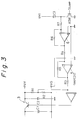
- Fig. 3 shows a power source for a thermal printer in accordance with another embodiment of the present invention.
- a differential amplifier 6 is used as an inverting amplifier of a gain -1.
- An analog switch ASW is turned on when signal T CLAMP shows value "1".
- Reference numeral C3 designates a capacitor for cutting or removing a direct current.
- signal T CLAMP shows value "1" while no thermal head prints characters.
- a feedback voltage from VH1 is corrected instead of VG1.
- a compensating circuit has differential amplifiers 4, 5 and resistors R3, R4, R5.
- the compensating circuit detects a load electric current supplied to a printer only within the power source and is constructed such that a reduction in voltage applied to the printer is compensated in accordance with the load electric current. Accordingly, the reduction in power voltage caused by an increase in printing amount is corrected by only a power source unit so that a stable voltage can be applied to the printer. Further, when the power source of the present invention is used for the printer, it is possible to prevent a defect in a connector and an excessive voltage from being caused in the printer and obtain printed characters having a uniform density.
Landscapes
- Electronic Switches (AREA)
- Control Or Security For Electrophotography (AREA)
Applications Claiming Priority (2)
| Application Number | Priority Date | Filing Date | Title |
|---|---|---|---|
| JP15794592 | 1992-06-17 | ||
| JP157945/92 | 1992-06-17 |
Publications (3)
| Publication Number | Publication Date |
|---|---|
| EP0574742A2 true EP0574742A2 (fr) | 1993-12-22 |
| EP0574742A3 EP0574742A3 (fr) | 1995-04-05 |
| EP0574742B1 EP0574742B1 (fr) | 1999-04-21 |
Family
ID=15660911
Family Applications (1)
| Application Number | Title | Priority Date | Filing Date |
|---|---|---|---|
| EP93108444A Expired - Lifetime EP0574742B1 (fr) | 1992-06-17 | 1993-05-25 | Soucre d'alimentation pour imprimante |
Country Status (4)
| Country | Link |
|---|---|
| US (1) | US5362161A (fr) |
| EP (1) | EP0574742B1 (fr) |
| CA (1) | CA2096778C (fr) |
| DE (1) | DE69324526T2 (fr) |
Families Citing this family (1)
| Publication number | Priority date | Publication date | Assignee | Title |
|---|---|---|---|---|
| US6481814B2 (en) | 2001-02-28 | 2002-11-19 | Lemark International, Inc. | Apparatus and method for ink jet printhead voltage fault protection |
Family Cites Families (8)
| Publication number | Priority date | Publication date | Assignee | Title |
|---|---|---|---|---|
| JPS55115185A (en) * | 1979-02-27 | 1980-09-04 | Omron Tateisi Electronics Co | Control unit for thermal print head |
| JPS58211471A (ja) * | 1982-06-04 | 1983-12-08 | Fuji Xerox Co Ltd | サ−マルヘツド駆動装置 |
| JPS59182757A (ja) * | 1983-04-01 | 1984-10-17 | Fuji Xerox Co Ltd | サ−マルプリンテイングヘツド用電源装置 |
| JPS61163874A (ja) * | 1985-01-16 | 1986-07-24 | Victor Co Of Japan Ltd | ライン熱印刷装置のヘツド駆動用電源保護回路 |
| JPS6232060A (ja) * | 1985-08-02 | 1987-02-12 | Mitsubishi Electric Corp | 記録ヘツド |
| JPS6327272A (ja) * | 1986-07-21 | 1988-02-04 | Terumo Corp | サーマルプリンタの通電制御回路 |
| JPS63242662A (ja) * | 1987-03-31 | 1988-10-07 | Victor Co Of Japan Ltd | 感熱転写階調制御装置 |
| JPS6450557A (en) * | 1987-08-21 | 1989-02-27 | Fujitsu Ltd | Infrared-ray detector array |
-
1993
- 1993-05-21 CA CA002096778A patent/CA2096778C/fr not_active Expired - Fee Related
- 1993-05-25 DE DE69324526T patent/DE69324526T2/de not_active Expired - Fee Related
- 1993-05-25 EP EP93108444A patent/EP0574742B1/fr not_active Expired - Lifetime
- 1993-05-26 US US08/067,034 patent/US5362161A/en not_active Expired - Lifetime
Also Published As
| Publication number | Publication date |
|---|---|
| EP0574742A3 (fr) | 1995-04-05 |
| EP0574742B1 (fr) | 1999-04-21 |
| US5362161A (en) | 1994-11-08 |
| DE69324526D1 (de) | 1999-05-27 |
| CA2096778C (fr) | 1999-01-19 |
| DE69324526T2 (de) | 1999-10-07 |
| CA2096778A1 (fr) | 1993-12-18 |
Similar Documents
| Publication | Publication Date | Title |
|---|---|---|
| EP1733410B1 (fr) | Systeme comprenant un fusible de securite pour vehicule et un convertisseur analogique/numerique | |
| JPH0542351B2 (fr) | ||
| EP0489909B1 (fr) | Compensation de resistance parasite pour imprimantes thermiques | |
| JP3322705B2 (ja) | サーマルプリンタ | |
| EP0217043B1 (fr) | Dispositif de détection d'erreurs dans le circuit de chauffage d'une tête d'impression thermique | |
| EP0499373A2 (fr) | Circuit de régulation d'énergie pour une tête d'impression thermique à jet d'encre | |
| EP0562626A1 (fr) | Tête d'imprimante dont les éléments chauffants sont reliés à des capteurs de courant | |
| JP3271633B2 (ja) | 位置検出回路 | |
| KR0167406B1 (ko) | 서멀 헤드 장치 | |
| EP0574742A2 (fr) | Soucre d'alimentation pour imprimante | |
| US5844581A (en) | Electronic control for consistent ink jet images | |
| US11485135B2 (en) | Print element substrate, printhead, and printing apparatus | |
| US4451835A (en) | Thermal recording device | |
| JPH0664207A (ja) | プリンタ用電源及びプリンタ | |
| JPH03146360A (ja) | サーマルヘッド断線検知回路 | |
| EP0537680A1 (fr) | Circuit de commande d'une tête d'impression thermique | |
| US5059986A (en) | Thermal head | |
| AU5427390A (en) | Electronic circuit arrangement | |
| JPH1134380A (ja) | サーマルヘッド駆動装置 | |
| US6616356B2 (en) | Method for controlling a thermal head to permit multicolor printing | |
| JP2521453B2 (ja) | サ−マルヘツド | |
| JPH0462555B2 (fr) | ||
| JPS63137861A (ja) | サ−マルプリント装置 | |
| JPH0214646B2 (fr) | ||
| JPH01128851A (ja) | サーマルプリントヘッドの印加電圧調整装置 |
Legal Events
| Date | Code | Title | Description |
|---|---|---|---|
| PUAI | Public reference made under article 153(3) epc to a published international application that has entered the european phase |
Free format text: ORIGINAL CODE: 0009012 |
|
| AK | Designated contracting states |
Kind code of ref document: A2 Designated state(s): DE FR GB |
|
| PUAL | Search report despatched |
Free format text: ORIGINAL CODE: 0009013 |
|
| AK | Designated contracting states |
Kind code of ref document: A3 Designated state(s): DE FR GB |
|
| 17P | Request for examination filed |
Effective date: 19950612 |
|
| 17Q | First examination report despatched |
Effective date: 19960301 |
|
| GRAG | Despatch of communication of intention to grant |
Free format text: ORIGINAL CODE: EPIDOS AGRA |
|
| GRAG | Despatch of communication of intention to grant |
Free format text: ORIGINAL CODE: EPIDOS AGRA |
|
| GRAH | Despatch of communication of intention to grant a patent |
Free format text: ORIGINAL CODE: EPIDOS IGRA |
|
| GRAH | Despatch of communication of intention to grant a patent |
Free format text: ORIGINAL CODE: EPIDOS IGRA |
|
| GRAA | (expected) grant |
Free format text: ORIGINAL CODE: 0009210 |
|
| AK | Designated contracting states |
Kind code of ref document: B1 Designated state(s): DE FR GB |
|
| REF | Corresponds to: |
Ref document number: 69324526 Country of ref document: DE Date of ref document: 19990527 |
|
| ET | Fr: translation filed | ||
| PLBE | No opposition filed within time limit |
Free format text: ORIGINAL CODE: 0009261 |
|
| 26N | No opposition filed | ||
| REG | Reference to a national code |
Ref country code: GB Ref legal event code: IF02 |
|
| PGFP | Annual fee paid to national office [announced via postgrant information from national office to epo] |
Ref country code: FR Payment date: 20090515 Year of fee payment: 17 Ref country code: DE Payment date: 20090527 Year of fee payment: 17 |
|
| PGFP | Annual fee paid to national office [announced via postgrant information from national office to epo] |
Ref country code: GB Payment date: 20090520 Year of fee payment: 17 |
|
| GBPC | Gb: european patent ceased through non-payment of renewal fee |
Effective date: 20100525 |
|
| REG | Reference to a national code |
Ref country code: FR Ref legal event code: ST Effective date: 20110131 |
|
| PG25 | Lapsed in a contracting state [announced via postgrant information from national office to epo] |
Ref country code: DE Free format text: LAPSE BECAUSE OF NON-PAYMENT OF DUE FEES Effective date: 20101201 |
|
| PG25 | Lapsed in a contracting state [announced via postgrant information from national office to epo] |
Ref country code: FR Free format text: LAPSE BECAUSE OF NON-PAYMENT OF DUE FEES Effective date: 20100531 |
|
| PG25 | Lapsed in a contracting state [announced via postgrant information from national office to epo] |
Ref country code: GB Free format text: LAPSE BECAUSE OF NON-PAYMENT OF DUE FEES Effective date: 20100525 |