EP0575171A2 - Verbesserte Systemverwaltungsverfahren und -vorrichtung - Google Patents
Verbesserte Systemverwaltungsverfahren und -vorrichtung Download PDFInfo
- Publication number
- EP0575171A2 EP0575171A2 EP93304730A EP93304730A EP0575171A2 EP 0575171 A2 EP0575171 A2 EP 0575171A2 EP 93304730 A EP93304730 A EP 93304730A EP 93304730 A EP93304730 A EP 93304730A EP 0575171 A2 EP0575171 A2 EP 0575171A2
- Authority
- EP
- European Patent Office
- Prior art keywords
- smm
- microprocessor
- circuitry
- routine
- memory
- Prior art date
- Legal status (The legal status is an assumption and is not a legal conclusion. Google has not performed a legal analysis and makes no representation as to the accuracy of the status listed.)
- Granted
Links
Images

Classifications
-
- G—PHYSICS
- G06—COMPUTING OR CALCULATING; COUNTING
- G06F—ELECTRIC DIGITAL DATA PROCESSING
- G06F9/00—Arrangements for program control, e.g. control units
- G06F9/06—Arrangements for program control, e.g. control units using stored programs, i.e. using an internal store of processing equipment to receive or retain programs
- G06F9/46—Multiprogramming arrangements
- G06F9/48—Program initiating; Program switching, e.g. by interrupt
- G06F9/4806—Task transfer initiation or dispatching
- G06F9/4812—Task transfer initiation or dispatching by interrupt, e.g. masked
-
- G—PHYSICS
- G06—COMPUTING OR CALCULATING; COUNTING
- G06F—ELECTRIC DIGITAL DATA PROCESSING
- G06F1/00—Details not covered by groups G06F3/00 - G06F13/00 and G06F21/00
- G06F1/24—Resetting means
-
- G—PHYSICS
- G06—COMPUTING OR CALCULATING; COUNTING
- G06F—ELECTRIC DIGITAL DATA PROCESSING
- G06F12/00—Accessing, addressing or allocating within memory systems or architectures
- G06F12/02—Addressing or allocation; Relocation
- G06F12/0223—User address space allocation, e.g. contiguous or non contiguous base addressing
Definitions
- This invention relates in general to electronic circuits, and more particularly to a microprocessor with enhanced system management mode (SMM) capabilities, including added functionality for recognizing NMI during SMM, buffering in SMM space I/O port information in response to an I/O trap, initiating SMM with a software instruction, and locking SMM configuration control.
- SMM system management mode
- the system management interrupt is provided on certain microprocessors (such as the Am386SXLV by Advanced Micro Devices of Austin, Texas, and the Intel 386SL microprocessor superset by Intel Corporation of Santa Clara, California).
- the SMI is non-maskable, and typically has a higher priority than the NMI (non-maskable interrupt).
- the Intel microprocessor superset maps a system management RAM (SM-RAM) address space into the memory space from 030000H-03FFFFH. All information relating to the current state of the microprocessor is saved to the SM-RAM area starting at address 3FFFFH and proceeding down in a stack-like fashion.
- the Intel microprocessor superset then begins executing in real mode at address 030000H.
- a resume (RSM) instruction the previous state of the processor is restored and program execution continues.
- the SM-RAM can be either dedicated RAM or part of the main memory. However, in the Intel microprocessor superset, the SM-RAM must occupy the address space between 30000H and 3FFFFH. This address space is accessible only when an SMI interrupt occurs, or if a bit (bit 3 of the OMDCR register) is set to a predetermined value.
- the purpose of the dedicated address space is to protect the SMI program from inadvertent overwriting by the application program, BIOS, operating system or other concurrently executing program.
- the Intel SL microprocessor superset restores the state of the CPU from system management memory, makes the normal memory accessible, and makes the SM-RAM inaccessible.
- the prior art SMI systems have several inherent faults.
- the prior art solutions store the entire state of the CPU automatically upon receiving an SMI interrupt. Consequently, each SMI entails a large time overhead for saving the information, whether or not the SMI routine requires saving the entire state of the microprocessor.
- SMI configuration is controlled by control registers values that, for example, enable SMI, and enable reads/writes to/from memory and/or SMI space. Because SMI operation is not subject to normal operating system protection mechanisms, unauthorized access to an SMI configuration control register, such as by a hacker or a virus, represents a serious protection hole. And fourth, in prior art systems, SMI can only be invoked by a hardware SMI interrupt.
- a microprocessor having enhanced system management circuitry is provided for diminishing substantial disadvantages associated with prior microprocessors.
- a microprocessor is coupled to memory, which may be separate from the microprocessor.
- the microprocessor includes circuitry for programmably defining a range of addresses within a selected address space of the memory, for storing system management routines. Access to the memory within the selected address space is provided in response to signals requesting a system management routine.
- the SMM may be customized to the SMI routines, such that excessive memory space is not wasted by the SMM, and the SMM may be provided in an area of the microprocessor's address space which will not affect other system or application programs.
- processor status information is programmably stored upon receiving an SMI request, such that the programmer can control what processor status information is saved.
- certain processor status information which will always be affected upon initiation of an SMI service routine is automatically stored. This aspect of the invention significantly reduces the minimum time overhead involved with regard to an SMI service routine.
- a computer system in another embodiment, includes a microprocessor and memory, where the microprocessor can operate in either normal mode or system management mode (SMM), and where SMM mode operation selectably includes one or more of the following features: (a) servicing NMIs during SMM operation; (b) locking access to SMM control information; (c) saving I/O trap information, and/or (d) initiating SMM operation with a software instruction.
- SMM mode operation selectably includes one or more of the following features: (a) servicing NMIs during SMM operation; (b) locking access to SMM control information; (c) saving I/O trap information, and/or (d) initiating SMM operation with a software instruction.
- the microprocessor includes circuitry that defines an SMM address space within a selected address space of the memory for use in executing SMM routines to perform SMM operations, and circuitry in the microprocessor that, in response to an SMI signal, invokes an SMM routine which performs a selected SMM operation and then returns the microprocessor to normal mode operation.
- the microprocessor may include circuitry for selectively enabling recognition of NMIs during SMM operations, such that, with NMI enabled, an SMM routine will execute the corresponding NMI handler routine, but with NMI not enabled, an SMM routine will not respond to the NMI interrupt, whereby the NMI interrupt can only be serviced after a return to normal mode operation.
- the microprocessor may include circuitry that defines SMM configuration information for SMM operations, including an SMM address space within a selected address space of the memory for use in executing SMM routines to perform SMM operations, and circuitry that, when an SMM lock state is enabled, prevents any activity other than an SMM routine from modifying SMM configuration information.
- the microprocessor may include circuitry that, during normal mode operations, stores I/O information about a current I/O operation in a temporary register, and circuitry that, in response to an SMI signal, invokes an SMM routine which performs a selected SMM operation including storing selected microprocessor status information within the SMM address space, including the I/O information from the temporary register.
- the I/O information comprises the associated operand, operand size, and port address for the I/O operation.
- the microprocessor may include circuitry that, in response to either (i) an SMI signal external to the microprocessor, or (ii) an SMI signal provided by software being executed by the microprocessor during normal mode operations, invokes an SMM routine which performs a selected SMM operation including programmably storing selected processor status information, and then returns the microprocessor to normal mode operation.
- the microprocessor status information saved during an SMM routine includes an indication of whether the SMM operation was initiated by software.
- the NMI servicing feature provides flexibility in servicing, during SMM operations, NMIs that may represent catastrophic failures.
- the SMM locking feature prevents unauthorized access to SMM space or SMM routines, such as by hackers or viruses.
- the I/O buffering feature facilitates transparent retries of I/O operations after SMM operations, such as for power-up of peripherals.
- the software SMM instruction provides added flexibility in the use of SMM operations.
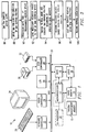
- FIGURE 1 illustrates a block diagram of a computer system.
- the computer system 10 comprises a microprocessor 12 coupled to a main memory 14, system management memory (SMM) 15 (analogous to the SM-RAM described above), BIOS ROM 16 and logic 18 (commonly referred to as the "chipset")
- SMM system management memory
- BIOS ROM 16 BIOS ROM 16
- logic 18 commonly referred to as the "chipset"
- Microprocessor 12 is coupled to bus 20.
- Bus 20 is used to communicate with a number of devices, shown in FIGURE 1 as keyboard controller 22, video controller 24, I/O circuitry 26 and disk controller 28.
- Keyboard controller 22 is coupled to keyboard 29.
- Disk controller 28 is coupled to hard disk 30 and floppy disk 32.
- Video controller 24 is coupled to display 34.
- An optional coprocessor 35 is coupled to microprocessor 12 and BIOS 16.
- the computer system 10 shown in FIGURE 1 is a general-purpose architecture common to personal computers such as the IBM Personal Computer and compatibles.
- the BIOS 16 (basic input/output system) is typically a read-only memory which contains a set of programs for performing the basic control and supervision operations for the computer system 10.
- the BIOS 16 acts as an interface between the computer circuitry and the application software being executed by the CPU 12.
- the BIOS 16 and logic 18 monitor the circuitry to determine whether power consumption reduction procedures may be invoked.
- the BIOS 16 and/or logic 18 may monitor the display 34 to determine whether its output has changed over a predetermined time period. If not, the BIOS 16 may invoke procedures to disable power to the display 34 (assuming computer system 10 is a portable computer) to conserve energy.
- BIOS 16 monitors microprocessor 12 to determine whether the microprocessor can be idled without affecting operation of the computer system 10. For example, the microprocessor 12 may be executing a routine to wait for a character from the keyboard. In this case, the operation of the microprocessor 12 can be suspended until a key is pressed.
- SMM 15 may be part of the main memory or a separate memory as shown in FIGURE 1. If SMM 15 is a separate memory, the corresponding address space of the main memory may be used for non-SMI purposes.
- FIGURE 2 illustrates a detailed block diagram of the various subcircuits of a preferred embodiment of the microprocessor 12.
- the microprocessor 12 will be described in connection with a microprocessor which is pin-compatible and instruction-compatible with the 80x86 family of processors by Intel Corporation, although the invention could be used in other processors as well.
- the microprocessor 12 comprises three main functional groups: the core circuitry 36, the memory circuitry 38 and the bus controller 40.
- the core circuitry 36 includes an instruction queue 42 coupled to an internal data bus 44.
- the output of the instruction queue 42 is coupled to a decoder 46 of the decode/sequence circuitry 47.
- the decode/sequence circuitry 47 also includes a sequencer 50 and an exception processor 86.
- the decoder 46 is coupled to a microcode ROM 48, exception processor 86 and sequencer 50.
- the sequencer 50 is also coupled to the microcode ROM 48 and to an execution unit 52.
- the execution unit includes a limit unit 54, a multiplier unit 56, an adder unit 58, a shift unit 60, and a register file 62.
- the execution unit 52 is coupled to the microcode ROM 48 and to multiplexer and I/O register circuitry 64.
- the memory circuitry 38 comprises a memory management unit 66 coupled to a linear address bus 68 which is also connected to the execution unit 52 and an instruction/data cache memory 70.
- Memory management unit 66 is further coupled to the internal data bus 44.
- a prefetch unit 72 is coupled between the memory management unit 66 and the cache 70.
- Bus controller 40 includes data buffers 74, address buffers 76 and control circuitry 78.
- the data buffers 74 are coupled to the data I/O pins D31-D0, the address buffers 76 are coupled to the address pins A31-A2 and BE3#-BE0# (for the 386DX bus architecture shown; a 386SX bus architecture would include address pins A24-A1 and BE[1:01]).
- a data address bus 80 couples the memory management unit 66, the cache 70 and the address buffer 76.
- An instruction address bus 82 couples the prefetch unit 72, cache 70 and address buffer 76.
- the data buffers 74 are coupled to the internal data bus 44.
- SMI System Management Interrupt
- SMADS System Management Address
- clock module 84 receives an external clock signal (CLK2) and generates CLKA (connected to the bus controller 40) and CLKB (coupled to the memory circuitry 38 and the core circuitry 36).
- CLKA and CLKB are both clock signals of one-half the frequency of CLK2.
- Clock module 84 receives control signals from bus controller 40. This structure provides for suspension of selected processor operations and is discussed in greater detail in connection in "Microprocessor with Hardware Controlled Power Management", Patent Application Serial No. 07/858,579, to Robert Maher et al., filed March 27, 1992, which is incorporated by reference herein.
- instructions are received by the microprocessor 12 from external memory under control of the memory management unit 66.
- an instruction/data cache 70 caches instruction and data received through the bus controller 40. Instructions are stored in the instruction queue and are subsequently translated by the decode circuitry 46 into microcode. The sequencer points to the next address in the microcode ROM 48 under control of the decoder 46 and the execution unit 52. The execution unit 52 processes information under control of the microcode ROM 48.
- the SMI pin is sampled active, indicating a request for the SMI service routine.
- the signal on the SMI pin must be active for at least four CLK2 periods to be recognized by the microprocessor 12 as a valid request.
- the microprocessor 12 recognizes an SMI interrupt input only when: (1) the SMI input pin is sampled active, (2) the SMM access bit (described below) is disabled, (3) the processor is not currently executing an SMI service routine, (4) SM4 bit (see Table 1) is set defining Address Region 4 as the SMM memory space, and (5) the size of Address Region 4 is defined (not disabled).
- the SMI pin is driven low by the microprocessor 12 until execution of the RSM instruction. Therefore, an external source cannot generate a second SMI until the current SMI service routine is complete.
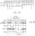
- FIGURE 3a Timing of the SMI handshake is shown in FIGURE 3a. Five significant events take place during the handshake. At “a”, SMI# input pin goes active (low). At “b”, the microprocessor samples SMI# active on the rising edge of CLK2 phase 1. At “c”, two CLK2s after sampling the SMI# active, the microprocessor switches the SMI# pin to an output and drives it low. At “d”, the microprocessor drives the SMI# pin high after RSM instruction has been executed indicating completion of the SMI service routine. At “e”, the microprocessor stops driving SMI# pin low and switches the SMI# pin to an input in preparation for the next SMI interrupt. The system is responsible for maintaining SMI# pin at an inactive level after the pin has been changed to an input.
- the microprocessor provides an SMI I/O trap mechanism which can be used to facilitate power management of I/O peripherals described in conjunction with the timing diagram of FIGURE 3b.
- SMI I/O trap mechanism which can be used to facilitate power management of I/O peripherals described in conjunction with the timing diagram of FIGURE 3b.
- the I/O address is driven onto the address bus. This address can be decoded by external logic. If a trap to the SMI handler is required, the SMI# input should be activated at least three CLK2 edges prior to returning the READY# input for the I/O cycle.
- the microprocessor immediately traps to the SMI interrupt handler following execution if the I/O instruction, and no other instructions are executed between completion of the I/O instruction and entering the SMI service routine.
- the I/O trap mechanism is not active during coprocessor accesses.
- the SMADS# functional timing, output delay times and float delay times are identical to the main memory address strobe (ADS#) timing.
- the SMI# input setup and hold times are identical to the timing for the NMI and INTR inputs.
- the SMI# output float delay times are identical to timing for the address bus outputs.
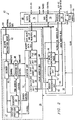
- the microprocessor 12 drives the SMI pin low in block 88.
- the SMADS output from the microprocessor 12 is activated (held low) to indicate that the current bus cycle is an SMM access and that the SMM address is present on the CPU address bus (A31-A2 and BE[3:0] for the 386DX bus architecture and A23-A1 and BE[1:0] for the 386SX bus architecture).
- the microprocessor 12 Upon detection of the falling edge of the SMI input, the microprocessor 12 maps the SMM to the programmed address space (described below in connection with Table 1) in block 90 and automatically saves the current and previous instruction pointers (EIP), CR0 register, EFLAGS register, DR7, code segment (CS) and the CS descriptor cache value current instruction REP prefix indicator (P), read/write string instruction indicator (I) and ESI (source memory) or EDI (destination memory) register in block 92.
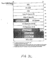
- the above-referenced values are stored to the top of the programmed SMM address space as shown in FIGURE 3c. These register values are saved automatically upon initiation of a SMI service routine because the microprocessor 12 always modifies these values upon entry to the SMI service routine.
- CR0, EFLAGS and DR7 are set to their reset values and the CS register is loaded with the base address and limits defined by the SMM configuration registers, described below.
- the full internal state of the microprocessor 12 can be saved to the SMM via execution of the normal MOV instruction and the SVDC, SVLDT and SVTS instructions, which are enhancements to the 386 and 486 instruction sets.
- the SVDC, SVLDT and SVTS instructions are used to store the segment registers, local descriptor table and task-state, respectively, and the associated descriptor cache contents in an 80-bit memory location which are not accessible to the programmer using the MOV command.
- the formats for the save instruction are as follows: SVDC mem80, Reg SVLDT mem80 SVTS mem80 where "mem80” refers to the 80-bit memory location in which the register value is to be saved. "Reg” specifies which register is to be saved (DS, ES, FS, GS, SS or CS).
- the SVDC, SVLDT and SVTS instructions allow the programmer greater control over the time delay between initiation of the SMI interrupt and the beginning of execution of the SMI service routine. Since, in the preferred embodiment, the microprocessor 12 is a static device, it will be unnecessary, in most cases, to save the full state of the microprocessor, since the state of the microprocessor is retained internally even with the clock input stopped. However, in the case where the system designer intends to shut off CPU power entirely, a full CPU state is required to resume operation where execution left off.
- the microprocessor begins the SMI service routine in real mode.
- the programmer must save the value of any registers that will be used by the service routine.
- the programmer For data access immediately after SMI entry, the programmer must use CS as a segment override. I/O port access is possible at the start of the routine, but the programmer must take care to save registers modified by the I/O instructions.
- the register and the register's descriptor cache contents can be saved using the SVDC instruction.
- memory and I/O accesses may take place. Data access to memory locations outside of the defined SMM memory space are issued with ADS# active rather than SMADS#. SMM memory accesses are automatically not cached.
- the processor may change from real mode to protected mode as required, and real or protected mode device drivers can be called.
- the registers values saved using the MOV, SVDC, SVLDC, SVLDT and SVTS instructions are restored using MOV, RSDC, RSLDT, and RSTS instructions, respectively.
- the RSDC, RSLDT and RSTS instructions are provided to allow reloading of the segment registers, LDT (local descriptor table) and TS (task state), respectively, and associated descriptor cache values that were stored using the SVDC, SVLDT and SVTS instructions.
- the formats for the restore instructions are as follows: RSDC Reg, mem80 RSLDT, mem80 RSTS, mem80 where Reg and mem80 are the selected register and 80-bit memory locations described above in connection with the SVDC, SVLDT and SVTS instructions.
- the SMI service routine ends with a RSM instruction.
- the values automatically saved responsive to the SMI input namely, the EIP, CR0 register, EFLAGS register, DR7, CS, CS descriptor cache values current instruction REP prefix indicator (P), read/write string instruction indicator (J) and ESI or EDI register, are restored and normal execution is resumed in block 100.
- the microprocessor 12 provides a plurality of configuration registers to store configuration data for the microprocessor 12.
- the configuration registers provide: (1) system management memory base address and SMM block size selections used to define the system management memory address space, (2) a system management memory access bit used to allow access to SMM without executing SMI, typically for initialization and test purposes, (3) a SMI enable bit used to enable the SMI and SMADS pins, and (4) a main memory access bit used to enable transfer of data to and from main memory that uses the same addresses as SMM while an SMI service routine is active or when the SMM address space is enabled via the SMACC control bit.
- Table 1 describes the configuration data stored in registers relevant to the control of SMI operations.
- the register index refers to the address of the register in a register file, described below in connection with FIGURE 4.
- Reset state 00h. CEh 7-0 Address bits A23-A16 of Region 4 starting address.
- Reset state 00h. CFh 7-4 Address bits A15-A12 of Region 4 starting address.
- Reset state 0h.
- Bit 7 of configuration control register 1 specifies wheter "adress region 4" defines the system management memory address region. If this bit is set to 1, address region 4 defines the SMM address region. The boundaries of the address space of address region 4 are further defined in connection with the address region 4 registers having indices CDH-CFH.
- Register CDH specifies address bits A31-A24 of region 4
- register CEH speciifies address bits A23-A16 of the region 4 starting address
- bits 7-4 of register CFH specifies address bits A15-A12 of the starting address of address region 4.
- Bits 3-0 of register index CFH specify the block size as specified in Table 1.
- register CDH would store the binary value "00000000”
- register CEH would store the value "00010000”
- register CFH would store the value "0000” in bits 7-4 and store the value "0110” in bits 3-0.
- Bit 7 of register C1H would be set to "1"
- This aspect of the present embodiment allows the system designer the flexibility to configure the SMM to a desired starting location and block size as needed.
- Configuration control register 1 (C1H) comprises three additional bits which affect operation of SMI service routines.
- Bit 3 of the configuration control register 1 is the MMACC (main memory access) bit. While the MMACC bit is set to "1", all data accesses that occur within a SMI service routine, or while the SMACC bit is set, will access main memory rather than SMM (code fetches will continue to access SMM).
- the SMACC (system memory access) bit (bit 2 of configuration control register 1) enables the SMM address space if the bit is set to "1". While enabled, any access (data or code fetch) to addresses within the defined SMM address space cause external bus cycles to be issued with the SMADS output active.
- Bit 1 of configuration control register 1 is the SMIEN (SMI enable) bit.
- SMIEN bit is set to "1"
- SMI and SMADS pins are enabled. If SMIEN is set to "0”, the SMI and SMADS pins are disconnected from the processor circuitry, i.e., the SMI input will not be recognized and the SMADS output will float. This aspect of the invention is described in greater detail below.
- FIGURE 4 illustrates the register file for storing the configuration data described in Table 1, along with the circuitry for reading and writing to the register file.
- the register file 102 is coupled to an index register 104 and a data register 106.
- the index and data registers are also coupled to internal data bus 44.
- the internal data bus 44 is also coupled to the bus controller 40, along with the internal address buses 80 and 82.
- An output from the register file 102 namely, the SMIEN signal, is coupled to the control inputs of tri-state devices 108 and 110.
- Tri-state device 108 is coupled between the bus controller and the SMADS pin.
- Bidirectional tri-state device 110 is coupled between the bus controller and the SMI pin.
- the SMIEN signal corresponds to the value of the SMIEN bit, i.e., bit 1 of register C1 of register file 102. If the SMIEN bit is equal to "1", then the tri-state devices 108-110 will be enabled; if not, the SMI and SMADS pins will be disabled. Since most processor pin-outs, including the 80386 DX and 80386 SX pin-outs, do not use all available pins on the chip package, the SMI and SMADS pins may be provided on the microprocessor chip without changing the pin-out of the chip package to maintain compatibility with the preexisting technology. However, in the preferred embodiment, these pins may be disabled by the SMIEN bit to ensure compatibility with a preexisting system design. In the preferred embodiment, the SMI and SMADS pins are initially disabled upon start-up of the microprocessor, and the BIOS 16 must be configured to enable the pins in its start-up routine, if desired.
- I/O port 23H is used to read data from, or write data to, the register. Each I/O port 23H operation must be preceded by an I/O port 22H operation, otherwise the second and later I/O port 23 operation will be directed off-chip.
- an optimal SMM address space may be defined which does not waste memory resources and which may be placed in the address space of the microprocessor such that it does not interfere with other system functions or application programs.
- the present invention automatically stores only the processor state information which will always be affected pursuant to initiation of a SMI service routine.
- Other processor state information which may not be affected during the SMI service routine is selectively saved by the programmer using the enhanced instructions.
- information that will not be affected during an SMI service routine need not be stored, thereby reducing the time overhead in performing an SMI service routine.
- the microprocessor 12 may implement additional optional features to provide: NMI ENABLE, SMI LOCK, I/O Trap Buffer, and SMINT.
- the microprocessor 12 includes an additional configuration control register CCR3.
- CCR3 can be used to programmably select (a) NMI ENABLE, and (b) SMI LOCK.
- the programmable NMI enable feature allows NMI events to be serviced in SMM (i.e., while an SMM routine is active).
- NMI can be enabled through the use of an NMI_ENABLE bit -- in the exemplary embodiment, bit 1 in a configuration control register CCR3. This bit will only affect NMI while an SMM routine is active -- otherwise the state of this control bit will have no affect on processing of NMI events.
- NMI_ENABLE bit is set to 0 (disabled).
- NMI_ENABLE is set prior to entering SMM, then an NMI event will be processed immediately independent of any SMM activity. If NMI_ENABLE is not set, as the microprocessor begins to execute microcode for an SMM routine, NMIs will be disabled from being serviced -- the exemplary microprocessor is capable of storing one NMI event while executing a SMI routine, but this event will not be serviced until a RSM instruction is executed or the NMI_ENABLE control bit is set.
- the programmable SMI LOCK feature allows the programmer to lock accesses to SMM control information. If the SMI_LOCK bit in CCR3 is set, SMM control information will be locked from any future modification by non-SMM operations.
- SMI_LOCK will prevent changes to the following SMM configuration control values: (a) CCR1 bits 1:3, 7, i.e., SMI enable (SMIEN), SMM memory access (SMACC), main memory access (MMACC), and the SMM address region (SM4); (b) the registers that define the SMM address space; and (c) CCR3 bit 1, i.e., SMI_LOCK.
- SMI_LOCK set, a non-SMM activity cannot access SMM space, nor modify the SMI_LOCK bit.
- SMI_LOCK remains active until the microprocessor is powered down, so that the lock once set will not be resettable by write accesses to CCR3. Once set, SMI_LOCK will be disabled during execution of an SMM handler, and then re-enabled upon completion of a RSM instruction.
- the microprocessor buffers this I/O information in a temporary register.
- the microprocessor traps to an SMM routine for powering-up the peripheral.
- the SMM routine will also save the I/O information -- data concatenated with port address and data size -- held in the temporary register.
- the programmer is then able to interrogate this I/O information prior to the execution of a RSM instruction -- for the exemplary embodiment, the saved I/O information is not part of the state information that is restored in response to RSM. This feature makes it easier to transparently implement SMM power management operations.
- the I/O information saved as state information is valid only for I/O write accesses (i.e., for read accesses, the read data would not be known).
- the I/O trap buffer feature can be used to facilitate SMM power management operations in general by, for example, invoking an SMM handler for all I/O operations (whether the peripheral is powered down or not), and then collecting the saved I/O state information to be used to facilitate powering-up a device after power management power-down.
- a map of state information saved to top of SMM memory in response to SMI interrupt, including I/O state information, is: DR7 -4h EFLAGS -8h CR0 -Ch CORE IP (Current IP) -10h ROM IP (Next IP) -14h Reserved (31:16)::CS Selector -18h CS Descriptor (63:32) -1Ch CS Descriptor (31:0) -20h Reserved (31:4)::S::P::I::C -24h OP Size::Port Address -28h Port Data -2Ch ESI or EDI -30h
- the present invention implements a software SMI instruction SMINT that can be used to invoke SMM.
- This instruction is mapped into a two byte opcode map, with the encoding 0F7E.
- CPL current privilege level
- SMIEN current privilege level
- SMACC set.
- the normal criterion to enable SMI includes having the SM4 bit (bit 7 of CCR1) set to designate address region 4 as SMI space, and to have this SMM region size greater than 0.
- the SMINT instruction invokes SMM is a manner equivalent to an SMI interrupt: the microprocessor automatically save off the state of chip to top of SMM memory space, and starts prefetching from the bottom of SMM space. Upon execution of RSM instruction the chip will return and continue operation from the point where software SMI instruction was executed.
- a status bit in the SMM memory map is set to indicate that the current SMM handler is being executed in response to software initiated interrupt.
- the PIC field in the SMM memory map shown in FIGURE 3c is expanded to an SPIC field (see the above memory map), where the S bit is used to identify if the SMM event was initiated by software or hardware.
- a software initiated SMM event the receipt of an external hardware SMI interrupt is latched, triggering a hardware initiated SMM operation after the software initiated SMM routine executes RSM.
- the SMI handshake will be honored and the SMI pin will be driven low until the hardware initiated SMI handler is complete and has executed a RSM instruction.
- SMI SMI interrupt routine
- SMACC SMI interrupt routine
- Instruction Opcode Format Description SVDC 0F78 SVDC mem80, reg Saves 'reg' contents and associated descriptor cache to 'mem80'.
- mem80 Restores 'reg' contents and associated descriptor cache from 'mem80'.
- Note CS is not allowed with RSDC but is allowed with SVDC.
- SVLDT 0F7A SVLDT mem80 Saves LDTR, Local Descriptor Table Register, to 'mem80', an 80-bit memory location.
- RSLDT 0F7B RSLDT mem80 Restores LDTR, Local Descriptor Table Register, from 'mem80', an 80-bit memory location.
- SVTS 0F7C SVTS mem80 Saves TSR, Task State Register, to 'mem80', an 80-bit memory location.
- RSTS 0F7D RSTS mem80 Restores TSR, Task State Register, from 'mem80', an 80-bit memory location.
- RSM 0FAA RSM Exits SMI service routine,. CPU state is restored from top of SMM space and execution resumes at interrupted point.
- SMINT 0F7E SMINT Calls SMI service routine. CPU state is saved to top of SMM space and execution will start from base of SMM space.
Landscapes
- Engineering & Computer Science (AREA)
- Theoretical Computer Science (AREA)
- Physics & Mathematics (AREA)
- General Engineering & Computer Science (AREA)
- General Physics & Mathematics (AREA)
- Software Systems (AREA)
- Microcomputers (AREA)
Applications Claiming Priority (4)
| Application Number | Priority Date | Filing Date | Title |
|---|---|---|---|
| US90005292A | 1992-06-17 | 1992-06-17 | |
| US900052 | 1992-06-17 | ||
| US6201493A | 1993-05-14 | 1993-05-14 | |
| US62014 | 1993-05-14 |
Publications (3)
| Publication Number | Publication Date |
|---|---|
| EP0575171A2 true EP0575171A2 (de) | 1993-12-22 |
| EP0575171A3 EP0575171A3 (de) | 1995-06-28 |
| EP0575171B1 EP0575171B1 (de) | 1999-10-13 |
Family
ID=26741765
Family Applications (1)
| Application Number | Title | Priority Date | Filing Date |
|---|---|---|---|
| EP93304730A Expired - Lifetime EP0575171B1 (de) | 1992-06-17 | 1993-06-17 | Verbesserte Systemverwaltungsverfahren und -vorrichtung |
Country Status (3)
| Country | Link |
|---|---|
| EP (1) | EP0575171B1 (de) |
| JP (1) | JPH06230979A (de) |
| DE (1) | DE69326718T2 (de) |
Cited By (9)
| Publication number | Priority date | Publication date | Assignee | Title |
|---|---|---|---|---|
| EP0617367A3 (de) * | 1993-03-22 | 1994-10-19 | Compaq Computer Corp | Systemverwaltungsunterbrechungsadressenbitkorrekturschaltung. |
| EP0609704A3 (de) * | 1993-02-01 | 1994-12-28 | Siemens Ag | Einrichtung zur Interruptsteuerung. |
| EP0695994A1 (de) * | 1994-07-25 | 1996-02-07 | Advanced Micro Devices, Inc. | Fehlerbeseitigungs- und Systemverwaltungsunterbrechung |
| WO1997013202A1 (en) * | 1995-10-06 | 1997-04-10 | Advanced Micro Devices, Inc. | Flexible implementation of a system management mode (smm) in a processor |
| EP0768603A3 (de) * | 1995-10-10 | 1997-12-29 | Cyrix Corporation | Ereignisverwaltungssystem |
| EP0902922A4 (de) * | 1996-06-04 | 2000-06-21 | Intel Corp | Verfahren und gerät zum zwischenspeichern von systemverwaltungsinformationen mit anderen informationen |
| EP0933704A3 (de) * | 1998-02-02 | 2002-12-04 | Texas Instruments Incorporated | Datenprozessor mit geschützten nichtmaskierbaren Unterbrechungen |
| US6711673B1 (en) * | 2000-01-03 | 2004-03-23 | Advanced Micro Devices, Inc. | Using a model specific register as a base I/O address register for embedded I/O registers in a processor |
| US9483426B2 (en) | 2012-01-31 | 2016-11-01 | Hewlett-Packard Development Company, L.P. | Locking a system management interrupt (SMI) enable register of a chipset |
Family Cites Families (5)
| Publication number | Priority date | Publication date | Assignee | Title |
|---|---|---|---|---|
| US4250546A (en) * | 1978-07-31 | 1981-02-10 | Motorola, Inc. | Fast interrupt method |
| US5228039A (en) * | 1990-05-09 | 1993-07-13 | Applied Microsystems Corporation | Source-level in-circuit software code debugging instrument |
| US5274791A (en) * | 1991-07-05 | 1993-12-28 | Chips And Technologies, Inc. | Microprocessor with OEM mode for power management with input/output intiated selection of special address space |
| US5274834A (en) * | 1991-08-30 | 1993-12-28 | Intel Corporation | Transparent system interrupts with integrated extended memory addressing |
| GB2259166B (en) * | 1991-08-30 | 1995-05-03 | Intel Corp | Transparent system interrupts with automated input/output trap restart |
-
1993
- 1993-06-15 JP JP14379793A patent/JPH06230979A/ja active Pending
- 1993-06-17 DE DE1993626718 patent/DE69326718T2/de not_active Expired - Fee Related
- 1993-06-17 EP EP93304730A patent/EP0575171B1/de not_active Expired - Lifetime
Cited By (11)
| Publication number | Priority date | Publication date | Assignee | Title |
|---|---|---|---|---|
| EP0609704A3 (de) * | 1993-02-01 | 1994-12-28 | Siemens Ag | Einrichtung zur Interruptsteuerung. |
| EP0617367A3 (de) * | 1993-03-22 | 1994-10-19 | Compaq Computer Corp | Systemverwaltungsunterbrechungsadressenbitkorrekturschaltung. |
| EP0695994A1 (de) * | 1994-07-25 | 1996-02-07 | Advanced Micro Devices, Inc. | Fehlerbeseitigungs- und Systemverwaltungsunterbrechung |
| US5623673A (en) * | 1994-07-25 | 1997-04-22 | Advanced Micro Devices, Inc. | System management mode and in-circuit emulation memory mapping and locking method |
| WO1997013202A1 (en) * | 1995-10-06 | 1997-04-10 | Advanced Micro Devices, Inc. | Flexible implementation of a system management mode (smm) in a processor |
| US6093213A (en) * | 1995-10-06 | 2000-07-25 | Advanced Micro Devices, Inc. | Flexible implementation of a system management mode (SMM) in a processor |
| EP0768603A3 (de) * | 1995-10-10 | 1997-12-29 | Cyrix Corporation | Ereignisverwaltungssystem |
| EP0902922A4 (de) * | 1996-06-04 | 2000-06-21 | Intel Corp | Verfahren und gerät zum zwischenspeichern von systemverwaltungsinformationen mit anderen informationen |
| EP0933704A3 (de) * | 1998-02-02 | 2002-12-04 | Texas Instruments Incorporated | Datenprozessor mit geschützten nichtmaskierbaren Unterbrechungen |
| US6711673B1 (en) * | 2000-01-03 | 2004-03-23 | Advanced Micro Devices, Inc. | Using a model specific register as a base I/O address register for embedded I/O registers in a processor |
| US9483426B2 (en) | 2012-01-31 | 2016-11-01 | Hewlett-Packard Development Company, L.P. | Locking a system management interrupt (SMI) enable register of a chipset |
Also Published As
| Publication number | Publication date |
|---|---|
| JPH06230979A (ja) | 1994-08-19 |
| DE69326718T2 (de) | 2000-11-16 |
| EP0575171A3 (de) | 1995-06-28 |
| DE69326718D1 (de) | 1999-11-18 |
| EP0575171B1 (de) | 1999-10-13 |
Similar Documents
| Publication | Publication Date | Title |
|---|---|---|
| JP4434482B2 (ja) | 仮想モードでのシステム管理モードサービスを実行する方法及び装置 | |
| US5729760A (en) | System for providing first type access to register if processor in first mode and second type access to register if processor not in first mode | |
| KR100403405B1 (ko) | 분산형버스액세스및제어조정에따라다수개의내부신호버스를공유하는다수개의회로기능요소를갖는집적회로 | |
| US6112303A (en) | Computer system with system ROM including serial-access PROM coupled to an auto-configuring memory controller and method of shadowing BIOS code from PROM | |
| CA1182927A (en) | Memory management arrangement for microprocessor systems | |
| EP0382470A2 (de) | Rechner mit Tastaturkennwortfunktionen | |
| US5634079A (en) | System for providing for a parallel port with standard signals and a flash recovery mode with second predetermined signals redefining parallel port with alternate functions | |
| US5737579A (en) | System and method for emulating computer architectures | |
| JP3869049B2 (ja) | コンピュータシステムにおけるスタンバイ中のデバイス構成のロス防止方法およびデバイス構成の捕捉のためのコントローラ回路 | |
| US5978903A (en) | Apparatus and method for automatically accessing a dynamic RAM for system management interrupt handling | |
| US6694401B2 (en) | Method and apparatus for executing real-mode interrupts from within extended SMRAM handler | |
| EP1256055A2 (de) | Rechnersystem mit einer speicherzugriffssteuerung zum gebrauch von non-system speicheraufschlagmitteln während systemurladungszeit | |
| US6775734B2 (en) | Memory access using system management interrupt and associated computer system | |
| JPS6055467A (ja) | マルチ・マイクロプロセツサによつて実現されたメインフレ−ム・エミユレ−シヨン用デ−タ処理システム | |
| US5509139A (en) | Circuit for disabling an address masking control signal using OR gate when a microprocessor is in a system management mode | |
| US5963738A (en) | Computer system for reading/writing system configuration using I/O instruction | |
| EP0575171B1 (de) | Verbesserte Systemverwaltungsverfahren und -vorrichtung | |
| US7178014B2 (en) | Method and apparatus for using a memory region to pass parameters between a run time environment and SMM handler | |
| US6282645B1 (en) | Computer system for reading/writing system configuration using I/O instruction | |
| JPS6097458A (ja) | デ−タ転送装置 | |
| WO2006069364A2 (en) | System and method for control registers accessed via private operations | |
| US6484227B1 (en) | Method and apparatus for overlapping programmable address regions | |
| US5392441A (en) | Pump bus to avoid indeterminacy in reading variable bit field | |
| US6339823B1 (en) | Method and apparatus for selective writing of incoherent MMX registers | |
| US5857116A (en) | Circuit for disabling an address masking control signal when a microprocessor is in a system management mode |
Legal Events
| Date | Code | Title | Description |
|---|---|---|---|
| PUAI | Public reference made under article 153(3) epc to a published international application that has entered the european phase |
Free format text: ORIGINAL CODE: 0009012 |
|
| AK | Designated contracting states |
Kind code of ref document: A2 Designated state(s): CH DE ES FR GB IE IT LI NL |
|
| PUAL | Search report despatched |
Free format text: ORIGINAL CODE: 0009013 |
|
| AK | Designated contracting states |
Kind code of ref document: A3 Designated state(s): CH DE ES FR GB IE IT LI NL |
|
| 17P | Request for examination filed |
Effective date: 19951214 |
|
| 17Q | First examination report despatched |
Effective date: 19970613 |
|
| GRAG | Despatch of communication of intention to grant |
Free format text: ORIGINAL CODE: EPIDOS AGRA |
|
| GRAG | Despatch of communication of intention to grant |
Free format text: ORIGINAL CODE: EPIDOS AGRA |
|
| GRAH | Despatch of communication of intention to grant a patent |
Free format text: ORIGINAL CODE: EPIDOS IGRA |
|
| GRAH | Despatch of communication of intention to grant a patent |
Free format text: ORIGINAL CODE: EPIDOS IGRA |
|
| GRAA | (expected) grant |
Free format text: ORIGINAL CODE: 0009210 |
|
| RAP1 | Party data changed (applicant data changed or rights of an application transferred) |
Owner name: NATIONAL SEMICONDUCTOR CORPORATION |
|
| AK | Designated contracting states |
Kind code of ref document: B1 Designated state(s): CH DE ES FR GB IE IT LI NL |
|
| PG25 | Lapsed in a contracting state [announced via postgrant information from national office to epo] |
Ref country code: NL Free format text: LAPSE BECAUSE OF FAILURE TO SUBMIT A TRANSLATION OF THE DESCRIPTION OR TO PAY THE FEE WITHIN THE PRESCRIBED TIME-LIMIT Effective date: 19991013 Ref country code: LI Free format text: LAPSE BECAUSE OF FAILURE TO SUBMIT A TRANSLATION OF THE DESCRIPTION OR TO PAY THE FEE WITHIN THE PRESCRIBED TIME-LIMIT Effective date: 19991013 Ref country code: IT Free format text: LAPSE BECAUSE OF FAILURE TO SUBMIT A TRANSLATION OF THE DESCRIPTION OR TO PAY THE FEE WITHIN THE PRE;WARNING: LAPSES OF ITALIAN PATENTS WITH EFFECTIVE DATE BEFORE 2007 MAY HAVE OCCURRED AT ANY TIME BEFORE 2007. THE CORRECT EFFECTIVE DATE MAY BE DIFFERENT FROM THE ONE RECORDED.SCRIBED TIME-LIMIT Effective date: 19991013 Ref country code: FR Free format text: LAPSE BECAUSE OF FAILURE TO SUBMIT A TRANSLATION OF THE DESCRIPTION OR TO PAY THE FEE WITHIN THE PRESCRIBED TIME-LIMIT Effective date: 19991013 Ref country code: ES Free format text: THE PATENT HAS BEEN ANNULLED BY A DECISION OF A NATIONAL AUTHORITY Effective date: 19991013 Ref country code: CH Free format text: LAPSE BECAUSE OF FAILURE TO SUBMIT A TRANSLATION OF THE DESCRIPTION OR TO PAY THE FEE WITHIN THE PRESCRIBED TIME-LIMIT Effective date: 19991013 |
|
| REG | Reference to a national code |
Ref country code: CH Ref legal event code: EP |
|
| REF | Corresponds to: |
Ref document number: 69326718 Country of ref document: DE Date of ref document: 19991118 |
|
| REG | Reference to a national code |
Ref country code: IE Ref legal event code: FG4D |
|
| EN | Fr: translation not filed | ||
| NLV1 | Nl: lapsed or annulled due to failure to fulfill the requirements of art. 29p and 29m of the patents act | ||
| REG | Reference to a national code |
Ref country code: CH Ref legal event code: PL |
|
| PG25 | Lapsed in a contracting state [announced via postgrant information from national office to epo] |
Ref country code: IE Free format text: LAPSE BECAUSE OF NON-PAYMENT OF DUE FEES Effective date: 20000617 Ref country code: GB Free format text: LAPSE BECAUSE OF NON-PAYMENT OF DUE FEES Effective date: 20000617 |
|
| PLBE | No opposition filed within time limit |
Free format text: ORIGINAL CODE: 0009261 |
|
| STAA | Information on the status of an ep patent application or granted ep patent |
Free format text: STATUS: NO OPPOSITION FILED WITHIN TIME LIMIT |
|
| 26N | No opposition filed | ||
| GBPC | Gb: european patent ceased through non-payment of renewal fee |
Effective date: 20000617 |
|
| PGFP | Annual fee paid to national office [announced via postgrant information from national office to epo] |
Ref country code: DE Payment date: 20010314 Year of fee payment: 8 |
|
| REG | Reference to a national code |
Ref country code: IE Ref legal event code: MM4A |
|
| PG25 | Lapsed in a contracting state [announced via postgrant information from national office to epo] |
Ref country code: DE Free format text: LAPSE BECAUSE OF NON-PAYMENT OF DUE FEES Effective date: 20020403 |