EP0576696A1 - Appareil et procédé pour la transformation et l'étalage à grande vitesse des images à deux ou trois dimensions, utilisant un système pipeline - Google Patents
Appareil et procédé pour la transformation et l'étalage à grande vitesse des images à deux ou trois dimensions, utilisant un système pipeline Download PDFInfo
- Publication number
- EP0576696A1 EP0576696A1 EP92110968A EP92110968A EP0576696A1 EP 0576696 A1 EP0576696 A1 EP 0576696A1 EP 92110968 A EP92110968 A EP 92110968A EP 92110968 A EP92110968 A EP 92110968A EP 0576696 A1 EP0576696 A1 EP 0576696A1
- Authority
- EP
- European Patent Office
- Prior art keywords
- image
- pixel
- images
- hardware
- transformation
- Prior art date
- Legal status (The legal status is an assumption and is not a legal conclusion. Google has not performed a legal analysis and makes no representation as to the accuracy of the status listed.)
- Ceased
Links
Images

Classifications
-
- G—PHYSICS
- G06—COMPUTING OR CALCULATING; COUNTING
- G06T—IMAGE DATA PROCESSING OR GENERATION, IN GENERAL
- G06T3/00—Geometric image transformations in the plane of the image
Definitions
- the invention applies to the field of Image Processing and specifically refers to an apparatus and method for manipulating bit-mapped images with a fast hardware engine capable to process images on pixel by pixel basis and to provide image 2D/3D translation, rotation, panning, zooming and shrinking at a high speed rate due to the pipelined implementation of such hardware.
- This hardware engine can be suitably interfaced to a host Graphic Workstation bus system to give this host the capability of performing 'Real Time Image Transformation and Display' function.
- a host Graphic Workstation bus system to give this host the capability of performing 'Real Time Image Transformation and Display' function.
- it means the ability of processing Monoband and Multiband images (i.e. RGB) of any size (up to 2048x2048 pixels) in few tenths of second.
- EP-A 0367418 by J.Gonzalez-Lopez describes an hardware engine that implements an image interpolation function providing a high speed zoom capability to an image display system, using a bi-dimensional filter.
- the apparatus disclosed in such application employs a bi-linear interpolation algorithm implemented in the form of cascaded one-dimensional interpolation circuits. It provides a single function, that is the image magnification.
- the present hardware solution allows a significant performance improvement adding the innovative solution of decomposing a complex image transformation in one or more simple passes with the aid of a Work Storage, a read path from this storage to Pixel Buffers, a Colour Look-Up Table (CLUT) function and an Average Mechanism.
- Another object of the present invention is to provide a Work Storage which can be smaller than the processed image, saving in this way hardware costs.
- the source image can be processed in several subsequent portions (called 'slices') which matches in size with the work storage size; this means that the overall passes for each image transformation must be repeated by the number of slices the image is divided by.
- the work storage size is limited by the fact that it does not impact the process speed and the image quality.
- Another object of the present invention is the possibility to "read back" a bit mapped image from the destination pixel memory to the source memory since the channel between the two memories is bi-directional.
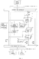
- Figure 1 shows how this hardware should be located inside a general purpose Graphic Workstation architecture to add this fast Image Processor to the basic graphics functions.
- FIG. 2 is the complete hardware diagram of the proposed invention.
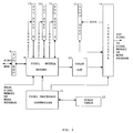
- Figure 3 represents one single band of the "Pixel Processor Pipeline” and is used to simplify the operation description; this is possible because in the complete fashion the single band hardware is merely triplicated to allow a RGB Image to be processed in the same time as a single band image.
- the "Image Processor” architecture in Figure 1 is comprised of two main logic blocks: Local Microprocessor Logic (4) and Pixel Processor Pipeline (5).
- Main function of this hardware is the mapping of an image, through a host system bus (3), from an input window located in the image source memory (2) to an output viewport located in the image destination memory (7), through a pixel memory bus (6), applying any 2D/3D spatial transformation.
- Pixel by pixel processing is performed by the Pixel Processor Pipeline (5) which takes advantage of the local processor power and programming capability to achieve a high degree of function flexibility with a negligible software overhead.
- Local Microprocessor Logic is controlled by the Host Processor (1) commands.
- a block diagram of the Pixel Processor Pipeline (5) hardware is shown in fig. 2 in the dotted box. It is comprised of the following blocks : The I/O Registers hardware block (8), which clocks pixel data transferred from or to the Host Bus Interface (3a).
- the Pixel Processor Controller hardware block (11) which controls the transfer of image pixels during the Pipeline process.
- the major tasks of this module are to provide control signals for the other hardware blocks, to compute the address of the pixels stored in the Pixel Buffers (10) and to compute the coefficients required by the Interpolators (14).
- the calculations of the above data are based on values stored in the Scale Table (12) and also on specific parameters for the image being processed.
- the Pixel Buffer Driver hardware block (9) controls the storage of the image rows coming from Image Source Memory (2) into three Pixel Buffers (10) and their transfer to the Colour Look Up Tables CLUT RAM memory (13).
- the main purpose of the Pixel Buffers (10) is to store pixels and combine the three colour bands so they can be processed in parallel.
- the sequence of pixel fetching from Image Source Memory (2) is the first row of the first band, the first row of the second band, the first row of the third band, the second row of the first band, and so on.
- the Pixel Buffers (10), under control of the Pixel Buffer Drivers (9), also provide the capability of re-sampling the source image data to perform the zoom and shrink functions.
- the CLUT's (13) provide the image colour transformation function during the image transfer through the Pixel Processor Pipeline (5). CLUT's are loaded with the proper values for the current Image function before the pipeline process begins. The number of CLUT entries to be loaded depends on the input pixel depth (1, 2, 4, 8, 12 bit/pixel). The CLUT can be loaded by the local Processor (4). A bit in the control register provides the capability for the processor to simultaneously load the three CLUT's with equal data. In this way it is possible to speed-up the CLUT loading time when identity or gray-scale values are requested.
- the CLUT can also be loaded directly from the system bus under hardware control with a significant increase in total speed and overall performance. This capability is particularly suitable when more than one image viewport is being displayed at a time and each viewport has a different CLUT.
- the Interpolator hardware block (14) provides continuous image zooming and shrinking in both horizontal and vertical directions simultaneously. For zooming, each new pixel is computed with an interpolation function (or replication function) between contiguous pixels in both X and Y directions. Selection between the 'interpolation' function or the 'pixel replication' function is made possible for both vertical and horizontal directions by means of suitable programming of Interpolators (14).
- the Average Buffers (15) are used by the Interpolators (14) to temporarily store the intermediate results of the averaging process activated for shrinking an image without loss of information (Smooth Shrink). Shrinking an image by skipping some of the input pixels may give poor results due to the loss of information.
- the averaging function generates output pixels by averaging the pixel values using the arithmetic mean within a rectangular window of the source image. The window dimensions is defined by the shrink scale factor. The output pixel is the arithmetic mean of all the pixels included in the window.
- the Pixel Processor hardware operation for a single colour band will be referred to Figures 2 and 3 remembering that, for processing RGB images, the three colour bands work in parallel with the same pixel flux.
- Figure 3 in particular, represents one of the three bands having the same process flux.
- the source image resides in a portion of the host memory called Image Source Memory (2).
- the Image Source Memory is accessed by the Local Processor (4) which performs the pixels fetching following a rule that comes from the specific image transformation to be done.
- the fetching rule should be one of the following : 'sequential row fetching' or 'sequential column fetching'.
- the local microprocessor is in charge of starting the pixel stream transfer but the pixels are moved by a hardware mechanism to achieve the required speed performance.
- Source pixels pass through the Host Bus Interface (3a), the I/O registers (8) and the Pixel Buffer Driver (9) and are stored into the Pixel Buffers (10).
- the process then continues through a pixels re-sampling from the Pixel Buffers (10), this re-sampling being controlled by the Pixel Processor Controller (11) by means of the Scale Table (12) data previously computed and stored by the Local Processor (4) for the actual transformation.
- the resampled pixels are sent down the pipeline through the CLUT (13) to the Interpolator (14) which generates the new pixels of the processed image.
- each single band has 3 Pixel Buffers capable of storing 3 image rows, this allows the mechanism described above to take place: while one out of 3 buffers holds pixels from the current fetched row, the other two buffers hold the previous two rows which are resampled and fed down to the pipeline for processing.
- Bi-linear interpolation works on four pixels at a time, two belonging to a first row and the other two belonging to a second row.
- the colour transformation through CLUT is accomplished before the interpolation step to achieve the generation of new pixels from real colour pixels instead of from indexed values.
- the new generated pixels from the interpolator go to the final Pixel Memory (7a) destination area for displaying or are temporarily stored in the Work Storage (7b) for further processing according to the required image transformation.
- the Pixel Memory (7a) and the Work Storage (7b) are accessed by the Pixel Memory Bus Interface logic (6a) which is able to address those memories for both write pixel and read pixel operations. Also these memories, as the Image Source Memory (2), can be read and written in sequence 'row by row' or 'column by column': these access modes are the basic scanning mechanism required to fully support all the 2D/3D transformations.
- each single pass takes place through the same set of processes performed by the hardware pipeline but with a unique set of hardware programming parameters for each specific pass.
- a fourth process step is the average mechanism which is activated only when the current pass needs to reduce the image size without a loss of information. This operation, called 'Smooth Shrink' is done by the Interpolator (14) who needs an external memory, the Average Buffer (15), for storing the accumulated pixel values from a computed number of image source rows and columns; those values will be averaged to generate the new final pixel.
- This specific hardware achieves a speed, limited only by the pipeline clock cycle, leading to the so called 'real time' operation, while the total process time to get the final result depends on the number of passes required by the specific function: the greater is the number of passes, the longer is the process time.
- a Texas Instruments TMS320C25 Digital Signal Processor is the local processor that is responsible for the overall control of the Image Display Feature hardware initialisation and operations. This processor supports real-time digital signal processing with a fast instruction cycle time of 100 nsec.
- the IDF microcode is loaded into the program memory during Initial Program Loading (IPL) time under the control of the host processor. Image commands and functional parameters from the host processor are stored in the Host Bus Interface memory.
- the DSP uses this information for calculating values for the CLUT and for initialising the IDF hardware for the next operation.
- the TMS320C25 DSP generates addresses for system bus operations, controls the flow of image functions, and handles internal and external interrupts.
- the processor has full read and write access to all hardware registers and all on-board memory.
- This IDF implementation uses a total of ten 1.5 and 2 micron CMOS gate arrays. There are two Host Bus Interface chips, one Pixel Processor Controller, three Pixel Buffer Drivers, three Interpolators, and one Pixel Memory Interface.
- Program and data memory are both implemented in fast access time (25 nsec) CMOS Static RAM to allow zero wait state access by the DSP.
- the IDF has 16K x 16 bits of program memory, three Pixel Buffers of 2K x 16 bits for each single band (total of 9 Buffers 2Kx16 bits for the 3 RGB bands), three CLUTs of 8K x 9 bits, 3 Average Buffers of 2K x 8 bits, and one Scale Table of 16K x 24 bits.
- Asynchronous FIFO's are used at the Video Pixel Memory bus interface to match the IDF pipeline rate of 100 nsec with the Video Pixel Memory bus rate of 80 nsec.
Landscapes
- Physics & Mathematics (AREA)
- General Physics & Mathematics (AREA)
- Engineering & Computer Science (AREA)
- Theoretical Computer Science (AREA)
- Image Processing (AREA)
- Image Generation (AREA)
- Processing Or Creating Images (AREA)
Priority Applications (3)
| Application Number | Priority Date | Filing Date | Title |
|---|---|---|---|
| EP92110968A EP0576696A1 (fr) | 1992-06-29 | 1992-06-29 | Appareil et procédé pour la transformation et l'étalage à grande vitesse des images à deux ou trois dimensions, utilisant un système pipeline |
| JP5105541A JPH06203167A (ja) | 1992-06-29 | 1993-05-06 | 高速2次元/3次元画像変換装置および方法 |
| US08/598,416 US6239812B1 (en) | 1992-06-29 | 1996-02-08 | Apparatus and method for high speed 2D/3D image transformation and display using a pipelined hardware |
Applications Claiming Priority (1)
| Application Number | Priority Date | Filing Date | Title |
|---|---|---|---|
| EP92110968A EP0576696A1 (fr) | 1992-06-29 | 1992-06-29 | Appareil et procédé pour la transformation et l'étalage à grande vitesse des images à deux ou trois dimensions, utilisant un système pipeline |
Publications (1)
| Publication Number | Publication Date |
|---|---|
| EP0576696A1 true EP0576696A1 (fr) | 1994-01-05 |
Family
ID=8209756
Family Applications (1)
| Application Number | Title | Priority Date | Filing Date |
|---|---|---|---|
| EP92110968A Ceased EP0576696A1 (fr) | 1992-06-29 | 1992-06-29 | Appareil et procédé pour la transformation et l'étalage à grande vitesse des images à deux ou trois dimensions, utilisant un système pipeline |
Country Status (3)
| Country | Link |
|---|---|
| US (1) | US6239812B1 (fr) |
| EP (1) | EP0576696A1 (fr) |
| JP (1) | JPH06203167A (fr) |
Families Citing this family (9)
| Publication number | Priority date | Publication date | Assignee | Title |
|---|---|---|---|---|
| US6806884B2 (en) * | 2001-09-25 | 2004-10-19 | Hewlett-Packard Development Company, L.P. | Technique for filling a region of memory using multiple region fill processors |
| US7050835B2 (en) * | 2001-12-12 | 2006-05-23 | Universal Display Corporation | Intelligent multi-media display communication system |
| US7109997B1 (en) | 2002-06-28 | 2006-09-19 | Microsoft Corporation | Systems and methods for direct storage of compressed scan converted data |
| US8432394B1 (en) | 2004-05-14 | 2013-04-30 | Nvidia Corporation | Method and system for implementing clamped z value interpolation in a raster stage of a graphics pipeline |
| US8411105B1 (en) | 2004-05-14 | 2013-04-02 | Nvidia Corporation | Method and system for computing pixel parameters |
| US8416242B1 (en) | 2004-05-14 | 2013-04-09 | Nvidia Corporation | Method and system for interpolating level-of-detail in graphics processors |
| US7079156B1 (en) * | 2004-05-14 | 2006-07-18 | Nvidia Corporation | Method and system for implementing multiple high precision and low precision interpolators for a graphics pipeline |
| US8441497B1 (en) | 2007-08-07 | 2013-05-14 | Nvidia Corporation | Interpolation of vertex attributes in a graphics processor |
| US8130229B2 (en) | 2009-11-17 | 2012-03-06 | Analog Devices, Inc. | Methods and apparatus for image processing at pixel rate |
Citations (4)
| Publication number | Priority date | Publication date | Assignee | Title |
|---|---|---|---|---|
| US4545069A (en) * | 1983-10-31 | 1985-10-01 | Xerox Corporation | Rotation of digital images |
| EP0367418A2 (fr) * | 1988-10-31 | 1990-05-09 | International Business Machines Corporation | Interpolateurs pour système d'affichage |
| EP0396517A1 (fr) * | 1989-04-28 | 1990-11-07 | International Business Machines Corporation | Méthode pour faire la convolution des images numériques |
| GB2244887A (en) * | 1990-04-11 | 1991-12-11 | Rank Cintel Ltd | Spatial transformation of video images |
Family Cites Families (7)
| Publication number | Priority date | Publication date | Assignee | Title |
|---|---|---|---|---|
| US5293481A (en) * | 1987-02-18 | 1994-03-08 | Canon Kabushiki Kaisha | Data parallel processing apparatus |
| JP2647375B2 (ja) * | 1987-02-18 | 1997-08-27 | キヤノン株式会社 | 画像処理装置 |
| DE68920144T2 (de) * | 1989-10-12 | 1995-06-29 | Ibm | Anzeigesystem. |
| US5097430A (en) * | 1990-01-16 | 1992-03-17 | Applied Materials, Inc. | Method and apparatus for displaying process end point signal based on emission concentration within a processing chamber |
| US5201035A (en) * | 1990-07-09 | 1993-04-06 | The United States Of America As Represented By The Secretary Of The Air Force | Dynamic algorithm selection for volume rendering, isocontour and body extraction within a multiple-instruction, multiple-data multiprocessor |
| JP2676116B2 (ja) * | 1990-09-18 | 1997-11-12 | 大日本スクリーン製造株式会社 | 画像データ処理方法および装置 |
| US5404445A (en) * | 1991-10-31 | 1995-04-04 | Toshiba America Information Systems, Inc. | External interface for a high performance graphics adapter allowing for graphics compatibility |
-
1992
- 1992-06-29 EP EP92110968A patent/EP0576696A1/fr not_active Ceased
-
1993
- 1993-05-06 JP JP5105541A patent/JPH06203167A/ja active Pending
-
1996
- 1996-02-08 US US08/598,416 patent/US6239812B1/en not_active Expired - Fee Related
Patent Citations (4)
| Publication number | Priority date | Publication date | Assignee | Title |
|---|---|---|---|---|
| US4545069A (en) * | 1983-10-31 | 1985-10-01 | Xerox Corporation | Rotation of digital images |
| EP0367418A2 (fr) * | 1988-10-31 | 1990-05-09 | International Business Machines Corporation | Interpolateurs pour système d'affichage |
| EP0396517A1 (fr) * | 1989-04-28 | 1990-11-07 | International Business Machines Corporation | Méthode pour faire la convolution des images numériques |
| GB2244887A (en) * | 1990-04-11 | 1991-12-11 | Rank Cintel Ltd | Spatial transformation of video images |
Non-Patent Citations (1)
| Title |
|---|
| ELECTRONIC DESIGN vol. 35, no. 14, 11 June 1987, HASBROUCK HEIGHTS, NEW JERSEY US pages 129 - 136 JOHN ELDON ET AL 'Image-resampling sequencer speeds graphics system design' * |
Also Published As
| Publication number | Publication date |
|---|---|
| JPH06203167A (ja) | 1994-07-22 |
| US6239812B1 (en) | 2001-05-29 |
Similar Documents
| Publication | Publication Date | Title |
|---|---|---|
| US5047760A (en) | Crossbar converter | |
| US5821940A (en) | Computer graphics vertex index cache system for polygons | |
| US5218674A (en) | Hardware bit block transfer operator in a graphics rendering processor | |
| US20100220103A1 (en) | Memory system and method for improved utilization of read and write bandwidth of a graphics processing system | |
| US6091429A (en) | Video/graphics memory system | |
| EP0576696A1 (fr) | Appareil et procédé pour la transformation et l'étalage à grande vitesse des images à deux ou trois dimensions, utilisant un système pipeline | |
| US6970170B2 (en) | Graphics resampling system and method for use thereof | |
| EP0658858B1 (fr) | Ordinateur graphique | |
| EP1345168B1 (fr) | Réglage dynamique de la densité d'échantillonnage et/ou de la fréquence de rendu dans un système graphique | |
| JPH1049666A (ja) | 断片発生器および断片発生方法 | |
| US7490208B1 (en) | Architecture for compact multi-ported register file | |
| US5670981A (en) | Method for mapping a source pixel image to a destination pixel space | |
| JPH05249953A (ja) | 画像表示装置 | |
| US6677950B1 (en) | Graphics computer | |
| GB2215956A (en) | Arbitrary shape clipper | |
| EP0775973B1 (fr) | Méthode et produit-programme informatique de transposition de données | |
| JP2613364B2 (ja) | 図形処理システム | |
| JP2000149054A (ja) | ボリュ―ムデ―タ集合の処理方法及びボリュ―ムレンダリングプロセッサ | |
| US6489967B1 (en) | Image formation apparatus and image formation method | |
| GB2215936A (en) | Video frame and rate conversion | |
| JP4482996B2 (ja) | データ記憶装置とその方法および画像処理装置 | |
| JP3247441B2 (ja) | 画像処理装置 | |
| GB2215955A (en) | Off screen memory | |
| JPH07129460A (ja) | 画像処理方法及びその装置 | |
| Srikanthan et al. | Transputer-based display management for a real-time vehicle simulator |
Legal Events
| Date | Code | Title | Description |
|---|---|---|---|
| PUAI | Public reference made under article 153(3) epc to a published international application that has entered the european phase |
Free format text: ORIGINAL CODE: 0009012 |
|
| AK | Designated contracting states |
Kind code of ref document: A1 Designated state(s): DE FR GB IT |
|
| 17P | Request for examination filed |
Effective date: 19940429 |
|
| 17Q | First examination report despatched |
Effective date: 19970507 |
|
| GRAG | Despatch of communication of intention to grant |
Free format text: ORIGINAL CODE: EPIDOS AGRA |
|
| STAA | Information on the status of an ep patent application or granted ep patent |
Free format text: STATUS: THE APPLICATION HAS BEEN REFUSED |
|
| 18R | Application refused |
Effective date: 19981010 |