EP0577080A1 - Méthode d'inspection de l'inclinaison d'un boîtier de circuit intégré - Google Patents
Méthode d'inspection de l'inclinaison d'un boîtier de circuit intégré Download PDFInfo
- Publication number
- EP0577080A1 EP0577080A1 EP93110372A EP93110372A EP0577080A1 EP 0577080 A1 EP0577080 A1 EP 0577080A1 EP 93110372 A EP93110372 A EP 93110372A EP 93110372 A EP93110372 A EP 93110372A EP 0577080 A1 EP0577080 A1 EP 0577080A1
- Authority
- EP
- European Patent Office
- Prior art keywords
- inclination
- open ends
- inspection
- inspection method
- representative point
- Prior art date
- Legal status (The legal status is an assumption and is not a legal conclusion. Google has not performed a legal analysis and makes no representation as to the accuracy of the status listed.)
- Granted
Links
Images

Classifications
-
- H—ELECTRICITY
- H10—SEMICONDUCTOR DEVICES; ELECTRIC SOLID-STATE DEVICES NOT OTHERWISE PROVIDED FOR
- H10P—GENERIC PROCESSES OR APPARATUS FOR THE MANUFACTURE OR TREATMENT OF DEVICES COVERED BY CLASS H10
- H10P72/00—Handling or holding of wafers, substrates or devices during manufacture or treatment thereof
- H10P72/50—Handling or holding of wafers, substrates or devices during manufacture or treatment thereof for positioning, orientation or alignment
- H10P72/53—Handling or holding of wafers, substrates or devices during manufacture or treatment thereof for positioning, orientation or alignment using optical controlling means
-
- H—ELECTRICITY
- H05—ELECTRIC TECHNIQUES NOT OTHERWISE PROVIDED FOR
- H05K—PRINTED CIRCUITS; CASINGS OR CONSTRUCTIONAL DETAILS OF ELECTRIC APPARATUS; MANUFACTURE OF ASSEMBLAGES OF ELECTRICAL COMPONENTS
- H05K13/00—Apparatus or processes specially adapted for manufacturing or adjusting assemblages of electric components
- H05K13/08—Monitoring manufacture of assemblages
- H05K13/081—Integration of optical monitoring devices in assembly lines; Processes using optical monitoring devices specially adapted for controlling devices or machines in assembly lines
- H05K13/0813—Controlling of single components prior to mounting, e.g. orientation, component geometry
Definitions
- the present invention relates to an inspection method of inclination of an IC to fix a position for mounting IC on a board.
- the present invention solves the above conventional problems, and it has a purpose to provide an inspection method of inclination of an IC in order to fix a position of IC speedily and precisely without the image information of binarized images.
- An inspection method of inclination of an IC defines a inspection area including open ends of IC pins on each side of IC package, extracts longitudinal edges and open ends of each IC pin from a density projection of each checking area, calculates a representative point of each checking area on a line along the open ends and calculates an inclination of an IC according to a difference of coordinates of a representative point of the checking area positioning on the opposite side.
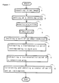
- Figure 1 is a flow chart showing an embodiment of the present invention.
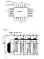
- Figure 2 is a conceptual diagram showing a setting of a checking area.
- Figure 3 is a conceptual diagram showing a point corresponding to a density projection, a primary differential and each pin of a checking area.
- Figure 4 is a diagram for explaining a position of an edge of a subpixel unit.
- Figure 5 is a conceptual diagram showing a center of an IC.
- Figure 1 is a flow chart showing an embodiment of the present invention.
- step 1 an image of IC with pins on 4 sides of QFT type etc. is taken on step 1.
- the value of density of the background and that of pin part have difference.
- checking ranges are set on the predetermined position in the image of IC and defines each of them as CR1 to CR4 ( Figure 2).
- One checking area is set in each side of IC, and there must be open ends of IC pins.
- a density projection of directions of X-axis and Y-axis of a checking area is generated on step 3.
- Figure 3 shows a density projection of a checking area CR1, which is an example.
- the density projection is data integrated multi-valued information of gray level of an image.
- the density projection has highly reliable information comparing with a binarized image lacking information on information compression.
- FIG. 3 shows the differential result by a thick line.
- a line along longitudinal edges of IC pins is emphasized, that is, the part to be emphasized is a boundary part of X-axis direction and a line along the open ends of IC pins, in other words, it is a boundary part of Y-axis direction (A boundary point is expressed by an "edge" hereafter.).
- a position of an edge is extracted by a subpixel unit, where a coordinate exists between subpixels.
- Figure 4 shows a part of the edge by a pixel unit of an image in a direction of Y-axis. It is usual that there are uneven in an image as Figure 4.
- subpixels In order to calculate more accurate position of the edge, that is Y-coordinates from such an image data, subpixels must be considered. As a result, it is possible to obtain a more exact and precise Y-coordinates ( Figure 6 shows a line of X-axis of the coordinates.) than the method obtaining coordinates by a pixel unit with the maximum value of a primary differential.
- the coordinates of a direction of X-axis is also calculated by a subpixel unit.
- the predetermined value calculated in experience is set as a threshold value, and a part is defined as an edge in the case the primary differential value is over the threshold value.
- a setting method of threshold value it is better to perform normarization after primary differential.
- a point corresponding to each IC pin is extracted.
- the point is represented by a cross point of a broken line showing a central point of a position of longitudinal edges of each pin and a thick line showing a position of an open edge of each pin as in Figure 3.
- the cross points are defined by P1 to Pn in the figure.
- a mean of a X-coordinates of points from P1 to Pn corresponding to each pin is calculated on X-axis, and it is defined as a representative point RP1 of a checking area CR1.
- step 8 lines connecting representative points positioning in the opposite side are calculated and defined as L1 and L2. Then, a crossing point of the lines is defined as a central point of the IC.
- An inclined angle can be calculated according to ⁇ Y/ ⁇ X when a difference of X-coordinates of RP1 and RP3 is defined as ⁇ X and a difference of a Y-coordinates of RP2 and RP4 is defined as ⁇ Y.
- the IC is rotated by the inclined angle defining the calculated center of IC as the center of it and its inclination is amended.
- the present invention mentioned above can exactly extract the inclination of an IC precisely in high speed without the information of binarized image, and amend the inclination after the extraction easily.
Landscapes
- Engineering & Computer Science (AREA)
- Operations Research (AREA)
- Manufacturing & Machinery (AREA)
- Microelectronics & Electronic Packaging (AREA)
- Image Processing (AREA)
- Image Analysis (AREA)
- Supply And Installment Of Electrical Components (AREA)
- Die Bonding (AREA)
- Length Measuring Devices By Optical Means (AREA)
Applications Claiming Priority (2)
| Application Number | Priority Date | Filing Date | Title |
|---|---|---|---|
| JP4194920A JP2851023B2 (ja) | 1992-06-29 | 1992-06-29 | Icの傾き検査方法 |
| JP194920/92 | 1992-06-29 |
Publications (2)
| Publication Number | Publication Date |
|---|---|
| EP0577080A1 true EP0577080A1 (fr) | 1994-01-05 |
| EP0577080B1 EP0577080B1 (fr) | 1997-04-02 |
Family
ID=16332546
Family Applications (1)
| Application Number | Title | Priority Date | Filing Date |
|---|---|---|---|
| EP93110372A Expired - Lifetime EP0577080B1 (fr) | 1992-06-29 | 1993-06-29 | Méthode d'inspection de l'inclinaison d'un boîtier de circuit intégré |
Country Status (4)
| Country | Link |
|---|---|
| US (1) | US5627912A (fr) |
| EP (1) | EP0577080B1 (fr) |
| JP (1) | JP2851023B2 (fr) |
| DE (1) | DE69309352T2 (fr) |
Cited By (4)
| Publication number | Priority date | Publication date | Assignee | Title |
|---|---|---|---|---|
| WO1996012395A1 (fr) * | 1994-10-12 | 1996-04-25 | Mydata Automation Ab | Reproduction compacte de composants |
| WO1996012396A1 (fr) * | 1994-10-12 | 1996-04-25 | Mydata Automation Ab | Reproduction d'images de composants |
| WO2002067198A1 (fr) * | 2001-02-20 | 2002-08-29 | Advantest Corporation | Procede d'appariement d'images, appareil d'appariement d'images et dispositif de traitement de tranches |
| EP3079452A4 (fr) * | 2013-12-02 | 2016-11-30 | Fuji Machine Mfg | Machine d'assemblage |
Families Citing this family (41)
| Publication number | Priority date | Publication date | Assignee | Title |
|---|---|---|---|---|
| US6090555A (en) * | 1997-12-11 | 2000-07-18 | Affymetrix, Inc. | Scanned image alignment systems and methods |
| US5631734A (en) * | 1994-02-10 | 1997-05-20 | Affymetrix, Inc. | Method and apparatus for detection of fluorescently labeled materials |
| US6741344B1 (en) * | 1994-02-10 | 2004-05-25 | Affymetrix, Inc. | Method and apparatus for detection of fluorescently labeled materials |
| JP3298753B2 (ja) * | 1994-10-14 | 2002-07-08 | 株式会社新川 | ワイヤ曲がり検査装置 |
| US6240218B1 (en) * | 1995-03-14 | 2001-05-29 | Cognex Corporation | Apparatus and method for determining the location and orientation of a reference feature in an image |
| JPH09189519A (ja) * | 1996-01-11 | 1997-07-22 | Ushio Inc | パターン検出方法およびマスクとワークの位置合わせ装置 |
| JPH09229642A (ja) * | 1996-02-27 | 1997-09-05 | Matsushita Electric Ind Co Ltd | 電子部品の外観検査方法 |
| US5999938A (en) * | 1997-01-31 | 1999-12-07 | Microsoft Corporation | System and method for creating a new data structure in memory populated with data from an existing data structure |
| US6424734B1 (en) | 1998-04-03 | 2002-07-23 | Cognex Corporation | Fiducial mark search using sub-models |
| US6324299B1 (en) | 1998-04-03 | 2001-11-27 | Cognex Corporation | Object image search using sub-models |
| US6252986B1 (en) | 1998-04-03 | 2001-06-26 | Cognex Corporation | Locating an image of an object having a concentric profile |
| US6411734B1 (en) | 1998-04-03 | 2002-06-25 | Cognex Corporation | Object image search using validated sub-model poses |
| US6516092B1 (en) | 1998-05-29 | 2003-02-04 | Cognex Corporation | Robust sub-model shape-finder |
| US7016539B1 (en) | 1998-07-13 | 2006-03-21 | Cognex Corporation | Method for fast, robust, multi-dimensional pattern recognition |
| US6963338B1 (en) | 1998-07-31 | 2005-11-08 | Cognex Corporation | Method for refining geometric description models using images |
| US6459820B1 (en) | 1998-08-25 | 2002-10-01 | Cognex Corporation | Gauging using sub-model poses |
| US6571006B1 (en) | 1998-11-30 | 2003-05-27 | Cognex Corporation | Methods and apparatuses for measuring an extent of a group of objects within an image |
| US6526165B1 (en) | 1998-11-30 | 2003-02-25 | Cognex Corporation | Methods and apparatuses for refining a geometric description of an object having a plurality of extensions |
| US6614926B1 (en) | 1999-06-29 | 2003-09-02 | Cognex Corporation | Methods and apparatuses for generating from an image a model of an object |
| US6898333B1 (en) | 1999-08-06 | 2005-05-24 | Cognex Corporation | Methods and apparatus for determining the orientation of an object in an image |
| US6813377B1 (en) | 1999-08-06 | 2004-11-02 | Cognex Corporation | Methods and apparatuses for generating a model of an object from an image of the object |
| US6542630B1 (en) * | 1999-09-14 | 2003-04-01 | Teradyne, Inc. | Inspecting component placement relative to component pads |
| US6950548B1 (en) | 2000-05-17 | 2005-09-27 | Cognex Corporation | Creating geometric model descriptions for use in machine vision inspection systems |
| DE60117930T2 (de) * | 2000-06-06 | 2006-10-05 | Agilent Technologies Inc., A Delaware Corp., Palo Alto | Verfahren und System zur automatischen Extraktion von Daten aus einem Molekülarray |
| US6591196B1 (en) * | 2000-06-06 | 2003-07-08 | Agilent Technologies Inc. | Method and system for extracting data from surface array deposited features |
| US6459807B1 (en) * | 2000-06-13 | 2002-10-01 | Semiconductor Technologies & Instruments, Inc. | System and method for locating irregular edges in image data |
| US6804416B1 (en) | 2001-03-16 | 2004-10-12 | Cognex Corporation | Method and system for aligning geometric object models with images |
| JP3698136B2 (ja) * | 2002-11-13 | 2005-09-21 | コニカミノルタビジネステクノロジーズ株式会社 | 画像処理装置および画像処理プログラム |
| US20040243341A1 (en) * | 2003-05-30 | 2004-12-02 | Le Cocq Christian A. | Feature extraction methods and systems |
| US7190834B2 (en) * | 2003-07-22 | 2007-03-13 | Cognex Technology And Investment Corporation | Methods for finding and characterizing a deformed pattern in an image |
| US8081820B2 (en) | 2003-07-22 | 2011-12-20 | Cognex Technology And Investment Corporation | Method for partitioning a pattern into optimized sub-patterns |
| JP4432474B2 (ja) * | 2003-11-27 | 2010-03-17 | ダイキン工業株式会社 | 遠心送風機の羽根車及びそれを備えた遠心送風機 |
| US20050281462A1 (en) * | 2004-06-16 | 2005-12-22 | Jayati Ghosh | System and method of automated processing of multiple microarray images |
| US7877213B2 (en) * | 2004-09-23 | 2011-01-25 | Agilent Technologies, Inc. | System and methods for automated processing of multiple chemical arrays |
| US8437502B1 (en) | 2004-09-25 | 2013-05-07 | Cognex Technology And Investment Corporation | General pose refinement and tracking tool |
| US9445025B2 (en) | 2006-01-27 | 2016-09-13 | Affymetrix, Inc. | System, method, and product for imaging probe arrays with small feature sizes |
| US8055098B2 (en) * | 2006-01-27 | 2011-11-08 | Affymetrix, Inc. | System, method, and product for imaging probe arrays with small feature sizes |
| JP2011232279A (ja) * | 2010-04-30 | 2011-11-17 | Sony Corp | 傾き検査装置及び傾き検査方法 |
| US9679224B2 (en) | 2013-06-28 | 2017-06-13 | Cognex Corporation | Semi-supervised method for training multiple pattern recognition and registration tool models |
| WO2015049723A1 (fr) * | 2013-10-01 | 2015-04-09 | 富士機械製造株式会社 | Machine d'assemblage |
| JP7797299B2 (ja) * | 2022-04-22 | 2026-01-13 | ヤマハ発動機株式会社 | 部品実装機、リード部品の位置算出方法およびリード部品の位置算出プログラム |
Citations (3)
| Publication number | Priority date | Publication date | Assignee | Title |
|---|---|---|---|---|
| EP0062335A2 (fr) * | 1981-04-03 | 1982-10-13 | Hitachi, Ltd. | Système de montage automatique |
| EP0222072A2 (fr) * | 1985-10-11 | 1987-05-20 | Hitachi, Ltd. | Méthode et appareil pour placer un dispositif monté en surface |
| EP0374848A2 (fr) * | 1988-12-20 | 1990-06-27 | Matsushita Electric Industrial Co., Ltd. | Dispositif de montage de circuits intégrés du type boîtier plat |
Family Cites Families (9)
| Publication number | Priority date | Publication date | Assignee | Title |
|---|---|---|---|---|
| CH643959A5 (de) * | 1978-04-14 | 1984-06-29 | Siemens Ag | Verfahren und vorrichtung zur automatischen lageerkennung von halbleiterchips. |
| US4696047A (en) * | 1985-02-28 | 1987-09-22 | Texas Instruments Incorporated | Apparatus for automatically inspecting electrical connecting pins |
| US5189707A (en) * | 1985-10-11 | 1993-02-23 | Hitachi, Ltd. | Method of loading surface mounted device and an apparatus therefor |
| US4969199A (en) * | 1986-02-28 | 1990-11-06 | Kabushiki Kaisha Toshiba | Apparatus for inspecting the molded case of an IC device |
| JPH077446B2 (ja) * | 1986-11-12 | 1995-01-30 | 松下電器産業株式会社 | 部品認識方法 |
| JPH01111281A (ja) * | 1987-10-23 | 1989-04-27 | Matsushita Electric Ind Co Ltd | 部品認識方法 |
| US5001766A (en) * | 1988-05-16 | 1991-03-19 | At&T Bell Laboratories | Apparatus and method for skew control of document images |
| JPH083405B2 (ja) * | 1989-06-30 | 1996-01-17 | 松下電器産業株式会社 | リード位置認識装置 |
| US5157734A (en) * | 1989-12-19 | 1992-10-20 | Industrial Technology Research Institute | Method and apparatus for picking and placing a surface mounted device with the aid of machine vision |
-
1992
- 1992-06-29 JP JP4194920A patent/JP2851023B2/ja not_active Expired - Fee Related
-
1993
- 1993-06-29 DE DE69309352T patent/DE69309352T2/de not_active Expired - Fee Related
- 1993-06-29 EP EP93110372A patent/EP0577080B1/fr not_active Expired - Lifetime
-
1995
- 1995-12-06 US US08/568,439 patent/US5627912A/en not_active Expired - Fee Related
Patent Citations (3)
| Publication number | Priority date | Publication date | Assignee | Title |
|---|---|---|---|---|
| EP0062335A2 (fr) * | 1981-04-03 | 1982-10-13 | Hitachi, Ltd. | Système de montage automatique |
| EP0222072A2 (fr) * | 1985-10-11 | 1987-05-20 | Hitachi, Ltd. | Méthode et appareil pour placer un dispositif monté en surface |
| EP0374848A2 (fr) * | 1988-12-20 | 1990-06-27 | Matsushita Electric Industrial Co., Ltd. | Dispositif de montage de circuits intégrés du type boîtier plat |
Cited By (4)
| Publication number | Priority date | Publication date | Assignee | Title |
|---|---|---|---|---|
| WO1996012395A1 (fr) * | 1994-10-12 | 1996-04-25 | Mydata Automation Ab | Reproduction compacte de composants |
| WO1996012396A1 (fr) * | 1994-10-12 | 1996-04-25 | Mydata Automation Ab | Reproduction d'images de composants |
| WO2002067198A1 (fr) * | 2001-02-20 | 2002-08-29 | Advantest Corporation | Procede d'appariement d'images, appareil d'appariement d'images et dispositif de traitement de tranches |
| EP3079452A4 (fr) * | 2013-12-02 | 2016-11-30 | Fuji Machine Mfg | Machine d'assemblage |
Also Published As
| Publication number | Publication date |
|---|---|
| JPH0618243A (ja) | 1994-01-25 |
| DE69309352D1 (de) | 1997-05-07 |
| US5627912A (en) | 1997-05-06 |
| EP0577080B1 (fr) | 1997-04-02 |
| JP2851023B2 (ja) | 1999-01-27 |
| DE69309352T2 (de) | 1997-07-10 |
Similar Documents
| Publication | Publication Date | Title |
|---|---|---|
| EP0577080B1 (fr) | Méthode d'inspection de l'inclinaison d'un boîtier de circuit intégré | |
| US5371690A (en) | Method and apparatus for inspection of surface mounted devices | |
| US5974169A (en) | Machine vision methods for determining characteristics of an object using boundary points and bounding regions | |
| US6771807B2 (en) | Method and system for detecting defects on a printed circuit board | |
| US7336813B2 (en) | System and method of determining image skew using connected components | |
| EP0807297B1 (fr) | Procede et appareil separant le premier plan de l'arriere-plan dans des images contenant du texte | |
| CN101127119B (zh) | 图案检查装置以及半导体检查系统 | |
| US5805722A (en) | Method and apparatus for locating, inspecting, and placing large leaded devices | |
| EP0573968A1 (fr) | Méthode d'inspection de l'inclinaison d'un circuit intégré | |
| CN112115948A (zh) | 一种基于深度学习的芯片表面字符识别方法 | |
| US8897538B1 (en) | Document image capturing and processing | |
| US5490084A (en) | Method and apparatus for detecting bent leads in electronic components | |
| JP6960252B2 (ja) | 画像分析装置及び鉄道設備部品の保守管理方法 | |
| CN118015079A (zh) | 光伏组件的定位方法、装置、设备及存储介质 | |
| US6526165B1 (en) | Methods and apparatuses for refining a geometric description of an object having a plurality of extensions | |
| JP3049488B2 (ja) | パターン検査方法及びパターン検査装置 | |
| CN116977721A (zh) | 一种贴片机自动示教的元件分类方法 | |
| JP3260425B2 (ja) | パターンのエッジライン推定方式及びパターン検査装置 | |
| JPH11328410A (ja) | パターンの位置合わせ方法 | |
| CN120852418B (zh) | 封装芯片球栅阵列的亚像素级检测方法及应用 | |
| CN114187294B (zh) | 基于先验信息的规则晶片定位方法 | |
| JPH1040393A (ja) | 画像認識方法およびこの方法を用いた画像認識装置ならびに電子部品実装装置 | |
| JPH10141930A (ja) | パターン検査方法及びパターン検査装置 | |
| JP3480642B2 (ja) | パターンの検査方法 | |
| KR100326257B1 (ko) | 와이어본딩을 위한 정렬패턴의 탐색 방법 |
Legal Events
| Date | Code | Title | Description |
|---|---|---|---|
| PUAI | Public reference made under article 153(3) epc to a published international application that has entered the european phase |
Free format text: ORIGINAL CODE: 0009012 |
|
| 17P | Request for examination filed |
Effective date: 19931022 |
|
| AK | Designated contracting states |
Kind code of ref document: A1 Designated state(s): DE FR GB |
|
| 17Q | First examination report despatched |
Effective date: 19950626 |
|
| RAP1 | Party data changed (applicant data changed or rights of an application transferred) |
Owner name: YOZAN INC. |
|
| GRAG | Despatch of communication of intention to grant |
Free format text: ORIGINAL CODE: EPIDOS AGRA |
|
| GRAH | Despatch of communication of intention to grant a patent |
Free format text: ORIGINAL CODE: EPIDOS IGRA |
|
| GRAH | Despatch of communication of intention to grant a patent |
Free format text: ORIGINAL CODE: EPIDOS IGRA |
|
| GRAA | (expected) grant |
Free format text: ORIGINAL CODE: 0009210 |
|
| AK | Designated contracting states |
Kind code of ref document: B1 Designated state(s): DE FR GB |
|
| REF | Corresponds to: |
Ref document number: 69309352 Country of ref document: DE Date of ref document: 19970507 |
|
| ET | Fr: translation filed | ||
| PGFP | Annual fee paid to national office [announced via postgrant information from national office to epo] |
Ref country code: DE Payment date: 19970730 Year of fee payment: 5 |
|
| PLBE | No opposition filed within time limit |
Free format text: ORIGINAL CODE: 0009261 |
|
| STAA | Information on the status of an ep patent application or granted ep patent |
Free format text: STATUS: NO OPPOSITION FILED WITHIN TIME LIMIT |
|
| 26N | No opposition filed | ||
| PGFP | Annual fee paid to national office [announced via postgrant information from national office to epo] |
Ref country code: GB Payment date: 19980526 Year of fee payment: 6 |
|
| PGFP | Annual fee paid to national office [announced via postgrant information from national office to epo] |
Ref country code: FR Payment date: 19980622 Year of fee payment: 6 |
|
| PG25 | Lapsed in a contracting state [announced via postgrant information from national office to epo] |
Ref country code: DE Free format text: LAPSE BECAUSE OF NON-PAYMENT OF DUE FEES Effective date: 19990401 |
|
| PG25 | Lapsed in a contracting state [announced via postgrant information from national office to epo] |
Ref country code: GB Free format text: LAPSE BECAUSE OF NON-PAYMENT OF DUE FEES Effective date: 19990629 |
|
| PG25 | Lapsed in a contracting state [announced via postgrant information from national office to epo] |
Ref country code: FR Free format text: THE PATENT HAS BEEN ANNULLED BY A DECISION OF A NATIONAL AUTHORITY Effective date: 19990630 |
|
| GBPC | Gb: european patent ceased through non-payment of renewal fee |
Effective date: 19990629 |
|
| REG | Reference to a national code |
Ref country code: FR Ref legal event code: ST |