EP0578548A1 - Unterbrechungsfreie Stromversorgungsanordnung mit Wechselspannungsausgang - Google Patents
Unterbrechungsfreie Stromversorgungsanordnung mit Wechselspannungsausgang Download PDFInfo
- Publication number
- EP0578548A1 EP0578548A1 EP93401719A EP93401719A EP0578548A1 EP 0578548 A1 EP0578548 A1 EP 0578548A1 EP 93401719 A EP93401719 A EP 93401719A EP 93401719 A EP93401719 A EP 93401719A EP 0578548 A1 EP0578548 A1 EP 0578548A1
- Authority
- EP
- European Patent Office
- Prior art keywords
- voltage
- inverter
- transformer
- transistors
- battery
- Prior art date
- Legal status (The legal status is an assumption and is not a legal conclusion. Google has not performed a legal analysis and makes no representation as to the accuracy of the status listed.)
- Withdrawn
Links
Images


Classifications
-
- H—ELECTRICITY
- H02—GENERATION; CONVERSION OR DISTRIBUTION OF ELECTRIC POWER
- H02J—ELECTRIC POWER NETWORKS; CIRCUIT ARRANGEMENTS OR SYSTEMS FOR SUPPLYING OR DISTRIBUTING ELECTRIC POWER; SYSTEMS FOR STORING ELECTRIC ENERGY
- H02J9/00—Circuit arrangements for emergency or stand-by power supply, e.g. for emergency lighting
- H02J9/04—Circuit arrangements for emergency or stand-by power supply, e.g. for emergency lighting in which the distribution system is disconnected from the normal source and connected to a standby source
- H02J9/06—Circuit arrangements for emergency or stand-by power supply, e.g. for emergency lighting in which the distribution system is disconnected from the normal source and connected to a standby source with automatic change-over, e.g. UPS systems
- H02J9/062—Circuit arrangements for emergency or stand-by power supply, e.g. for emergency lighting in which the distribution system is disconnected from the normal source and connected to a standby source with automatic change-over, e.g. UPS systems for AC powered loads
Definitions
- the invention relates to a linear back-up electrical supply device with alternating output voltage, this device being intended in particular to be interposed between an electrical distribution network and an electronic device such as for example an information processing device. .
- these devices include an inverter associated with an electric storage battery and controlled to supplement the electric voltage normally supplied by a distribution network, in the event of a micro-cut, cut or disappearance of this voltage.
- Transformers are provided at the input and / or output to supply a regulated alternating voltage to the device to be supplied.
- the object of the invention is in particular to simplify the aforementioned devices and to reduce their size, their weight and their cost price.
- It relates to a supply device of the aforementioned type, which comprises only one transformer.
- a backup electrical power supply device with alternating output voltage this device being intended in particular to be interposed between an electrical distribution network and an electronic device such as an information processing device, and comprising a rectifier supplied by the distribution network and connected to the terminals of an inverter such as a power stage with transistors of the push-pull type, a battery of electric accumulators to supply the inverter in the event of interruption or disappearance of the electrical voltage supplied by the distribution network, and a transformer whose secondary winding delivers the desired alternative output voltage, characterized in that it comprises a bridge assembly, two branches of which are connected to the same rectifier output terminal, comprising the transistors of an inverter, the other two branches of which are connected to the other output terminal of the rectifier each have do a controlled switch whose diagonal comprises the primary winding of the transformer, as well as means for controlling the transistors of the inverter and the controlled switches so that, in the presence of the voltage supplied by the network, the rectified voltage supplied by the rectifier is applied alternately in one direction and in the other
- the device according to the invention makes it possible to supply an electronic device with a sinusoidal voltage regulated from the rectified voltage of the network, by driving a bridge of transistors operating in linear mode and of controlled switches. The yield under these conditions is excellent.
- this device includes only one transformer. This results in a gain in weight, volume and price compared to the prior devices.
- the device comprises only one inverter and in the event of a cut or disappearance of the network voltage, the controlled switches are open (the device then being reduced to a push-pull circuit) and the transistors of the inverter continue to be controlled alternately by the aforementioned control means, to generate an alternating voltage across the secondary winding of the transformer from the direct voltage supplied by the battery.
- the battery is preferably connected to the primary winding of the transformer by a controlled switch, which is open in the presence of the mains voltage and which is closed in the event of a cut or disappearance of the mains voltage.
- a filtering capacitor is connected between the output terminals of the rectifier, the filtered rectified voltage which is thus supplied being greater than the battery voltage.
- the transistors of the inverter can be controlled at any frequency to supply the device connected to the device with an alternating voltage having a frequency independent of the grid frequency.
- the device comprises two inverters in parallel, the first inverter being in the bridge arrangement, the second inverter being connected to the terminals of a second primary winding of the aforementioned transformer, this second winding being in parallel with the first, the second inverter being supplied by the battery in the event of disappearance or drop in the voltage supplied by the network, the first inverter operating alone in the presence of the voltage supplied by the network.
- This second embodiment of the device according to the invention makes it possible to improve the operation on a reactive load.
- the inverters can also be controlled so that the two operate in parallel on the battery.
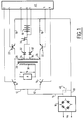
- FIG. 1 in which the general structure of an embodiment of the device according to the invention has been shown schematically.
- This device comprises a rectifier 10, such as a diode bridge, comprising two input terminals to which the voltage Ve applied by the electrical distribution network is applied and two output terminals between which a bridge mounting of a inverter and two controlled switches, with the primary winding of an output transformer connected across the bridge.
- a rectifier 10 such as a diode bridge
- this bridge includes two branches 12 which are connected to the same output terminal 14 of the rectifier 10 and which each comprise a controlled switch 16, such as for example a transistor controlled in all or nothing.
- the two other branches 18 of the bridge are connected to the other output terminal 20 of the rectifier and each comprise a transistor (for example of the MOS-FET type) 22 whose emitter is connected to the output terminal 20 of the rectifier and whose the collector is connected to the diagonal 24 of the bridge, in which is connected the primary winding 26 of a transformer 28 whose secondary winding 30 provides a regulated output voltage Vs which is applied to the supply terminals of a device to supply A, such as a micro- or mini-computer for example.
- a transistor for example of the MOS-FET type
- a battery B of electric accumulators has an output terminal connected to the output terminal 20 of the rectifier 10 and another output terminal connected to the primary winding 26 of the transformer by two diodes 32 connected in parallel and whose cathodes are connected to taps 34 of the primary winding, which are symmetrical with respect to the midpoint of this winding and positioned to keep the same number of volts per turn in the presence of the mains voltage Ve or in the presence of the battery voltage, as is will see in more detail below.
- a controlled switch 36 such as a thyristor is interposed between the battery B and the diodes 32.
- control terminals of the controlled switches 16 are connected to outputs 1 and 2 of a control card 40 also comprising two outputs 3 and 4 connected to the bases of the transistors 22 to drive the latter, an output 5 connected to the control terminal the controlled switch or thyristor 36, and two terminals 6, 7 connected to the terminals of the battery B to control the voltage thereof.
- control card 40 comprises input terminals of the network voltage Ve and terminals for controlling the output voltage Vs and the output current.
- the device which has just been described operates as follows: in the presence of the mains voltage Ve, and when this remains between two predetermined values (for example ⁇ 10% relative to the nominal voltage), the controlled switch 36 is open to isolate the battery B from the primary winding 26 of the transformer.
- the controlled switches 16 and the transistors 22 operating in linear mode are controlled, alternately, by the control card 40 so that the double-wave rectified corrugated voltage supplied by the rectifier 10 from the network voltage Ve is applied in one direction. , then in the other to the primary winding of the transformer to generate an alternating output voltage Vs across the terminals of the secondary winding 30 of the transformer.
- one of the controlled switches 16 is open while the other is closed and simultaneously the transistor 22 located in the branch of the bridge directly connected to the branch containing the open switch 16 is conductive while that the transistor 22 located in the other branch of the bridge, connected directly to the branch of the bridge comprising the switch 16 closed, is blocked.
- the current supplied by the rectifier 10 flows in the branch of the bridge comprising the closed switch 16 then in the primary winding 26 of the transformer and in the branch of the bridge comprising the conductive transistor 22.
- the switch 16 which was open is closed, while the switch 16 which was closed is open and simultaneously, the transistor 22 which was conductive is blocked, while the other transistor 22 which was blocked is conductive, and the current then flows in the other direction in the primary winding 26 of the transformer.
- a regulated alternating voltage Vs is generated at the terminals of the secondary winding 30 which is synchronous and in phase with the network voltage Ve.
- the micro-cuts, interruptions or disappearances of the network voltage Ve, as well as its variations beyond the predetermined limits are detected by the control card 40 which then opens the two controlled switches 16 and commands the closing of the controlled switch or thyristor 36 , while continuing to drive the transistors 22. These are driven by the same single-wave corrugated voltages as before, represented in FIGS. 2 and 3, which are supplied by the control card 40 and which were synchronous with the network voltage Ve, to produce a regulated sinusoidal voltage Vs.
- the voltage shown in Figure 2 is supplied for example to terminal 3 of the control card 40 while the voltage of Figure 3 is supplied to terminal 4 of this control card.
- the switch 36 being closed, the current supplied by the battery B passes through a diode 32, circulates in a part of the primary winding 26 and passes through the transistor 22 whose base receives from the control card 40 a control voltage formed by a regulated sinusoid arch with a low distortion rate as shown at the start of the curve in FIG. 2.
- this control voltage becomes zero, it is the other transistor 22 which receives on its base a voltage of piloting constituted by a regulated sinusoid arch with a low distortion rate, and the current supplied by the battery then passes through the other diode 32 and flows in the primary winding towards this transistor 22.
- the two transistors 22 thus mounted form a power stage of the push-pull type and constitute an inverter with the primary winding of the transformer.
- the connection points 34 of the diodes 32 on the primary winding are determined so that the number of volts per turn remains constant when it is the rectified corrugated voltage supplied by the rectifier 10 which circulates in all the primary winding 26 or when c 'is the voltage supplied by the battery which circulates in a part of this primary winding, between a connection point 34 and the end of the primary winding 24 connected to the collector of the corresponding transistor 22.
- This makes it possible in particular to use a battery B providing an output voltage adapted to the different use cases (for example 48 volts or 98 volts).
- FIG. 4 shows a second embodiment of the device according to the invention, and in which the battery B is associated with a second inverter mounted in parallel with the first and connected across a second primary winding 26 'of the transformer 28, this second primary winding 26' being in parallel with the first primary winding 26.
- the device according to the invention comprises, as in the first embodiment, a rectifier 10 connected to the terminals of the network and receiving the input voltage Ve, a bridge mounting of two transistors 16 and of the two transistors 22 of the first cited inverter, with the first primary winding 26 of the transformer 28 in the diagonal of this bridge arrangement.
- the second inverter is of the same type as the first inverter and comprises a push-pull circuit of transistors 22 ', operating in linear mode and controlled by the control card 40 in the same way as the transistors 22 of the first inverter.
- the positive terminal of the battery B is connected to the midpoint of the second primary winding 26 'of the transformer, its negative terminal being connected to the emitters of the transistors 22', possibly via a protection diode.
- this device in the presence of the voltage Ve supplied by the network, the transistors 22 of the first inverter and the transistors 16 are controlled in linear mode as already described for the transistors 22 of the first embodiment of FIG. 1.
- the transistors 16 are blocked by the control card 40, and the transistors 22 'of the second inverter are controlled exactly like the transistors 22 of the first inverter.
- the voltage Vs supplied to the apparatus A connected to the terminals of the secondary winding 30 of the transformer 28, is a sinusoidal voltage regulated exactly as in the case of the embodiment of FIG. 1.
- the two inverters operate alternately, under control of the card 40: in the presence of the voltage Ve supplied by the network, the transistors 22 'of the second inverter are blocked and vice versa when the voltage Ve disappears or becomes less than a limit value, the transistors 16 are blocked and transistors 22 are possibly blocked.
- the two inverters can also be controlled in parallel on the battery so that, in the presence of the grid voltage Ve, only the first inverter operates and, in the event of a drop or disappearance of the voltage Ve, the two inverters are supplied by the battery and operate in parallel to supply the voltage Vs on the secondary winding of the transformer.
- the variant embodiment shown in FIG. 5 is substantially identical to the embodiment of the FIG. 4, but the transistors 16 of the two upper branches of the bridge function as switches and are controlled in all or nothing by the voltage in slots Vc represented in FIG. 7.
- This control voltage Vc is defined on the basis of the positive or negative sign of the instantaneous power at the terminals of the primary winding 26 of the transformer 28.
- FIG. 6 the shape of the voltage Vp and of the current Ip is shown in this primary winding.
- the voltage Vc for controlling the switches 16 is equal to a predetermined non-zero value.
- the control voltage Vc of the switches 16 is equal to 0.
- This control mode is well suited to supplying a reactive load A, for which the current and the voltage are out of phase.
- FIG. 5 works exactly like that of FIG. 4.
- FIG. 8 represents another variant embodiment of the device according to the invention, which differs from that of FIG. 4 in that the two controlled transistors or switches 16 are omitted, the upper output terminal of the rectifier 10 being connected directly to the point middle of the primary winding 26 of the transformer 28.
- the device is identical to that of FIG. 4, and the transistors 22, 22 ′ of the inverters are controlled in the same way as those of FIG. 4.
- the yield of the device according to the invention is excellent and reaches 90% in the presence of mains voltage.
- the sinusoidal output voltage Vs generated from the mains voltage is regulated and filtered from any disturbance, distortion or overvoltage.
- the control card 40 controls the network voltage Ve and the output voltage Vs so as to regulate the output voltage Vs for example to ⁇ 5% of its nominal value, for variations of ⁇ 10% of the network voltage Ve relative to at its nominal value.
- the control voltages of the transistors 22, 22 ′ which are generated by the control card 40, make it possible to eliminate all disturbances, distortion rates and overvoltages of the network voltage.
- the micro-cuts, interruptions and disappearances of the line voltage are immediately compensated by the battery B after opening of the controlled switches or transistors 16.
- the total response time is less than a millisecond, so that no disturbance can alter the alternating voltage of Vs output, the transformer leakage self-inductors completely masking the effects of this response time.
- the control card 40 is also designed to, in the event of an overload, manage the operating points of the transistors 22, 22 'to maintain them in their safety areas, these transistors being dimensioned to accept thirty times their nominal current for ten half-wave voltage, which provides a very large supply of the inrush currents required by electronic devices A.
- the control card 40 also controls the voltage of the battery and the charging thereof by means of a conventional charging circuit, such as a switching power supply for example.
- control card 40 The circuits of the control card 40 are within the reach of those skilled in the art and have already been described in the aforementioned prior patents of the applicant, to which it suffices to refer.
- this control card can also be of the microprocessor type as shown diagrammatically in FIG. 9 and then comprises two microprocessors 42 and 44 connected to each other and receiving the voltage Ve, the first microprocessor 42 being responsible for generating and synchronize the control voltages to supply them to the bases of the transistors 22 or 22 'on its outputs 3 and 4 and to control the switches 16 by its output terminals 1 and 2.
- the second microprocessor 44 is responsible for controlling the switch 36 by its output terminal 5, to control the voltage of the battery by its terminals 6 and 7, to control the voltage and the output current at the terminals of the secondary winding of the transformer by its terminals 8 and 9, and to control the battery charging circuit 46.
- the second microprocessor 44 can also have other functions, such as the display of the battery voltage, the output current and the network or battery operation, the storage of calibration parameters and the management of a memory.
- one of these microprocessors can be used to determine the peak current admissible by the transistors 22 of the inverter at the start of an electronic load such as a microcomputer, for example.
- FIG. 10 shows the equivalent diagram of an electronic load designated by the reference A, and in FIG. 11 the shape of the voltages and of the current at start-up during the first half-wave of the output voltage of the inverter. During this first half-wave, the device only supplies current when the output voltage Vs is greater than the voltage Vcl of the capacitor C1, ie for a short duration which can be of the order of 1 ms.
- the microprocessor of the control card measures this conduction time and determines, as a function of this duration, the peak current admissible by the transistors 22, while the conventional control cards take into account the duration of the half-wave, i.e. 10 ms. It is thus possible to ensure the start-up of electronic systems requiring high VA (volt-amperes), with an efficient low-power inverter and capable of delivering current form factors of 8 or 10 (the current supplied at start-up being represented by I D in figure 11).
- the frequency of the output voltage Vs is then independent of that of the network voltage Ve, and is determined by the frequency of the control voltage of the transistors 22. It is thus possible to adjust the frequency of the output voltage Vs to any desired value.
- control card 40 includes an additional output providing the same control voltage as above, but phase shifted by 120 °.
- the three devices according to the invention are connected together so that the phase-shifted voltage of a first device serves as voltage reference driver for another device. This produces a single-phase inverter.
Landscapes
- Business, Economics & Management (AREA)
- Emergency Management (AREA)
- Engineering & Computer Science (AREA)
- Power Engineering (AREA)
- Charge And Discharge Circuits For Batteries Or The Like (AREA)
- Inverter Devices (AREA)
Applications Claiming Priority (2)
| Application Number | Priority Date | Filing Date | Title |
|---|---|---|---|
| FR9208305A FR2693322B1 (fr) | 1992-07-06 | 1992-07-06 | Dispositif d'alimentation électrique secourue à tension de sortie alternative. |
| FR9208305 | 1992-07-06 |
Publications (1)
| Publication Number | Publication Date |
|---|---|
| EP0578548A1 true EP0578548A1 (de) | 1994-01-12 |
Family
ID=9431575
Family Applications (1)
| Application Number | Title | Priority Date | Filing Date |
|---|---|---|---|
| EP93401719A Withdrawn EP0578548A1 (de) | 1992-07-06 | 1993-07-02 | Unterbrechungsfreie Stromversorgungsanordnung mit Wechselspannungsausgang |
Country Status (3)
| Country | Link |
|---|---|
| EP (1) | EP0578548A1 (de) |
| JP (1) | JPH0698562A (de) |
| FR (1) | FR2693322B1 (de) |
Cited By (2)
| Publication number | Priority date | Publication date | Assignee | Title |
|---|---|---|---|---|
| GB2292273A (en) * | 1994-08-10 | 1996-02-14 | Dien Ghing Hsin | Switching power supply operable on dual/multiple voltage level inputs; UPS |
| DE102017106224A1 (de) | 2016-03-24 | 2017-09-28 | Sma Solar Technology Ag | Wechselrichter und Steuerverfahren für einen Wechselrichter |
Citations (6)
| Publication number | Priority date | Publication date | Assignee | Title |
|---|---|---|---|---|
| GB2120474A (en) * | 1982-05-11 | 1983-11-30 | Harmer & Simmons Ltd | Standby power supply system |
| EP0200656A1 (de) * | 1985-05-03 | 1986-11-05 | Societe Generale De Travaux Electriques | Unterbrechungsfreie Wechselstromversorgung mit einer Kraft von 1500 VA oder weniger |
| EP0237369A1 (de) * | 1986-02-06 | 1987-09-16 | SERRAS-PAULET, Edouard | Elektrisches Speisegerät mit Wechselspannungsausgang |
| US4780801A (en) * | 1987-01-15 | 1988-10-25 | M-Power, Inc. | Uninterruptible power supply apparatus |
| US5010469A (en) * | 1990-05-09 | 1991-04-23 | Albar | Uninterruptible power supply with dual level voltage input |
| WO1991012645A1 (fr) * | 1990-02-19 | 1991-08-22 | Serras Paulet Edouard | Procede et dispositif d'alimentation et de protection d'un appareil electronique, en particulier d'un appareil informatique |
-
1992
- 1992-07-06 FR FR9208305A patent/FR2693322B1/fr not_active Expired - Fee Related
-
1993
- 1993-07-02 EP EP93401719A patent/EP0578548A1/de not_active Withdrawn
- 1993-07-06 JP JP5166642A patent/JPH0698562A/ja active Pending
Patent Citations (7)
| Publication number | Priority date | Publication date | Assignee | Title |
|---|---|---|---|---|
| GB2120474A (en) * | 1982-05-11 | 1983-11-30 | Harmer & Simmons Ltd | Standby power supply system |
| EP0200656A1 (de) * | 1985-05-03 | 1986-11-05 | Societe Generale De Travaux Electriques | Unterbrechungsfreie Wechselstromversorgung mit einer Kraft von 1500 VA oder weniger |
| EP0237369A1 (de) * | 1986-02-06 | 1987-09-16 | SERRAS-PAULET, Edouard | Elektrisches Speisegerät mit Wechselspannungsausgang |
| US4780801A (en) * | 1987-01-15 | 1988-10-25 | M-Power, Inc. | Uninterruptible power supply apparatus |
| WO1991012645A1 (fr) * | 1990-02-19 | 1991-08-22 | Serras Paulet Edouard | Procede et dispositif d'alimentation et de protection d'un appareil electronique, en particulier d'un appareil informatique |
| EP0443917A1 (de) * | 1990-02-19 | 1991-08-28 | SERRAS-PAULET, Edouard | Verfahren und Vorrichtung für Stromversorgung und Schutz von einem elektronischen Apparat, insbesondere Datenverarbeitungsgerät |
| US5010469A (en) * | 1990-05-09 | 1991-04-23 | Albar | Uninterruptible power supply with dual level voltage input |
Cited By (4)
| Publication number | Priority date | Publication date | Assignee | Title |
|---|---|---|---|---|
| GB2292273A (en) * | 1994-08-10 | 1996-02-14 | Dien Ghing Hsin | Switching power supply operable on dual/multiple voltage level inputs; UPS |
| GB2292273B (en) * | 1994-08-10 | 1999-07-07 | Dien Ghing Hsin | Switching power supply |
| DE102017106224A1 (de) | 2016-03-24 | 2017-09-28 | Sma Solar Technology Ag | Wechselrichter und Steuerverfahren für einen Wechselrichter |
| US10447175B2 (en) | 2016-03-24 | 2019-10-15 | Sma Solar Technology Ag | Inverter and control method for an inverter |
Also Published As
| Publication number | Publication date |
|---|---|
| FR2693322A1 (fr) | 1994-01-07 |
| FR2693322B1 (fr) | 1994-09-30 |
| JPH0698562A (ja) | 1994-04-08 |
Similar Documents
| Publication | Publication Date | Title |
|---|---|---|
| EP0654887B1 (de) | Unterbrechungsfreie Stromversorgung mit gemeinsamem Nullleiter und Doppelaufwärtskonverter | |
| EP2351188B1 (de) | Ununterbrechbare gleichstrom-stromversorgungseinrichtung für ein datenverarbeitungssystem mit mindestens einem prozessor | |
| FR2577728A1 (fr) | Dispositif d'alimentation en energie stabilisee | |
| EP0410866B1 (de) | Vorrichtung für Energieumwandlung mit Mehrfachausgang | |
| FR2845211A1 (fr) | Systeme et procede de conversion vers un facteur de puissance eleve | |
| FR2568715A1 (fr) | Dispositif de commande d'une bobine d'electroaimant et appareil electrique de commutation equipe d'un tel dispositif | |
| FR2947969A1 (fr) | Nouvelle architecture de compensateur des facteurs de puissance et d'harmoniques pour reseau de distribution d'energie | |
| CA1265193A (fr) | Appareil d'alimentation electrique a sortie de tension alternative | |
| EP0578548A1 (de) | Unterbrechungsfreie Stromversorgungsanordnung mit Wechselspannungsausgang | |
| EP0169756A1 (de) | Stabilisierte elektrische Stromversorgung | |
| EP0795224B1 (de) | Versorgungsanlage für die hilfstromkreise einer ferngespeisten pumpstation | |
| EP0035727A1 (de) | Energieversorgungssystem für elektronische Anlagen | |
| FR2581488A1 (fr) | Perfectionnement aux alimentations en courant alternatif non susceptibles d'etre interrompues | |
| WO1989001256A1 (fr) | Appareil d'alimentation electrique a sortie de tension alternative regulee | |
| EP1177613B1 (de) | Telefonleitungsgespeistes stromversorgungssystem | |
| EP4014309B1 (de) | Induktive halteschaltung | |
| FR2730104A1 (fr) | Alimentation continue a correcteur de facteur de puissance et convertisseur a decoupage utilisable dans une telle alimentation | |
| FR2694144A1 (fr) | Convertisseur pour charge réversible. | |
| CA1264806A (fr) | Procede et convertisseur pour l'alimentation en courant continu d'une pluralite de charges electriques | |
| EP4465482A1 (de) | Unterbrechungsfreie stromversorgungsschaltung mit abwärts- und aufwärtswandler | |
| EP0270450B1 (de) | Niederspannungsversorgungsschaltung ohne Netzspannungsabwärtstransformator | |
| EP0600809A1 (de) | Wechselstrom-dynamische Ausgleichvorrichtung | |
| EP0443917A1 (de) | Verfahren und Vorrichtung für Stromversorgung und Schutz von einem elektronischen Apparat, insbesondere Datenverarbeitungsgerät | |
| EP2131483A1 (de) | Geschwindigkeitsregler mit Superkondensator | |
| FR2634329A1 (fr) | Dispositif d'alimentation electrique secourue |
Legal Events
| Date | Code | Title | Description |
|---|---|---|---|
| PUAI | Public reference made under article 153(3) epc to a published international application that has entered the european phase |
Free format text: ORIGINAL CODE: 0009012 |
|
| AK | Designated contracting states |
Kind code of ref document: A1 Designated state(s): AT BE CH DE DK ES FR GB GR IE IT LI NL PT SE |
|
| 17P | Request for examination filed |
Effective date: 19940701 |
|
| STAA | Information on the status of an ep patent application or granted ep patent |
Free format text: STATUS: THE APPLICATION IS DEEMED TO BE WITHDRAWN |
|
| 18D | Application deemed to be withdrawn |
Effective date: 19960201 |