EP0579855A1 - Circuit de compensation de temps de propagation - Google Patents
Circuit de compensation de temps de propagation Download PDFInfo
- Publication number
- EP0579855A1 EP0579855A1 EP92112607A EP92112607A EP0579855A1 EP 0579855 A1 EP0579855 A1 EP 0579855A1 EP 92112607 A EP92112607 A EP 92112607A EP 92112607 A EP92112607 A EP 92112607A EP 0579855 A1 EP0579855 A1 EP 0579855A1
- Authority
- EP
- European Patent Office
- Prior art keywords
- delay
- circuit
- output
- input
- arrangement according
- Prior art date
- Legal status (The legal status is an assumption and is not a legal conclusion. Google has not performed a legal analysis and makes no representation as to the accuracy of the status listed.)
- Withdrawn
Links
- 239000004065 semiconductor Substances 0.000 claims description 8
- 238000004519 manufacturing process Methods 0.000 claims description 6
- 230000005669 field effect Effects 0.000 claims 2
- 238000011156 evaluation Methods 0.000 claims 1
- 238000000034 method Methods 0.000 abstract description 7
- 230000008569 process Effects 0.000 abstract description 7
- 230000003213 activating effect Effects 0.000 abstract 1
- 230000000737 periodic effect Effects 0.000 description 4
- 230000008901 benefit Effects 0.000 description 2
- 230000004913 activation Effects 0.000 description 1
- 230000008859 change Effects 0.000 description 1
- 238000010276 construction Methods 0.000 description 1
- 238000010586 diagram Methods 0.000 description 1
- 230000000694 effects Effects 0.000 description 1
- 230000006870 function Effects 0.000 description 1
- 238000005259 measurement Methods 0.000 description 1
Images
Classifications
-
- H—ELECTRICITY
- H03—ELECTRONIC CIRCUITRY
- H03K—PULSE TECHNIQUE
- H03K5/00—Manipulating of pulses not covered by one of the other main groups of this subclass
- H03K5/13—Arrangements having a single output and transforming input signals into pulses delivered at desired time intervals
- H03K5/133—Arrangements having a single output and transforming input signals into pulses delivered at desired time intervals using a chain of active delay devices
-
- H—ELECTRICITY
- H03—ELECTRONIC CIRCUITRY
- H03K—PULSE TECHNIQUE
- H03K5/00—Manipulating of pulses not covered by one of the other main groups of this subclass
- H03K2005/00013—Delay, i.e. output pulse is delayed after input pulse and pulse length of output pulse is dependent on pulse length of input pulse
- H03K2005/00078—Fixed delay
- H03K2005/00097—Avoiding variations of delay using feedback, e.g. controlled by a PLL
-
- H—ELECTRICITY
- H03—ELECTRONIC CIRCUITRY
- H03K—PULSE TECHNIQUE
- H03K5/00—Manipulating of pulses not covered by one of the other main groups of this subclass
- H03K2005/00013—Delay, i.e. output pulse is delayed after input pulse and pulse length of output pulse is dependent on pulse length of input pulse
- H03K2005/0015—Layout of the delay element
- H03K2005/00195—Layout of the delay element using FET's
Definitions
- the invention relates to a delay discriminator circuit according to the preamble of claim 1.
- fast digital integrated semiconductor circuits As are used, for example, in the memory area for graphics or video applications, it is desirable to ensure a defined and as long as possible hold time for output signals, the hold time being the time within the data on a data line. Since the edges of the signals cannot be made steep as a result of peak current requirements, there is a fundamental conflict with the usual requirement for the shortest possible delay times, that is to say the times it takes for the signal to change to a stable state after activation for the same signals. In addition, the values of the hold times and the delay times of such fast digital integrated semiconductor circuits fluctuate due to process variations during manufacture. Usually, blocks with excessive delay times are then discarded, while tolerances according to values smaller than those specified do not pose any problems for manufacturers and customers. If certain non-zero positive hold times are specified, however, modules that turn out to be particularly fast copies due to the process scatter must also be discarded, since these fast hold times can no longer be processed by subsequent circuit parts.
- the present invention is therefore based on the object of specifying a circuit arrangement in order to avoid the loss of yield in fast digital integrated semiconductor circuits.
- the advantage of the invention is that by introducing a delay circuit into the signal path, which has different adjustable delay times, the process-related fluctuations of such faster digital semiconductor circuits are compensated, thereby increasing the yield during manufacture.
- Another advantage lies in the fact that if a simple automatic delay discriminator circuit is provided, the digitally controllable delay circuit can easily be automatically adapted to the delay behavior of the signals.
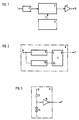
- FIG. 1 shows an input terminal 1 to which a clock signal can be applied.
- This input terminal 1 is connected to a functional unit 2, which generates a data signal.
- This data signal is fed to the input of the switchable delay circuit 3.
- the output signal of the switchable delay circuit 3 is fed to an output terminal 5 via a driver stage 4.
- a runtime discriminator circuit is designated 6. Its output signal 7 is fed to the control input of the controllable delay circuit 3.
- the runtime discriminator circuit 6 shown in FIG. 2 contains an input terminal 8 to which any periodic or non-periodic clock cycle, as may be present in digital integrated circuits, can be supplied.
- This input terminal 8 is connected to the input of a first delay element 9 and to the input of a second delay element 10.
- the output of the first delay element 9 is connected to the data input D of a flip-flop 11.
- the output of the delay element 10 is also connected to the clock input CL of the D flip-flop 11.
- the control signal 7 can be tapped at the output Q of the D flip-flop 11.
- the manual delay discriminator circuit shown in FIG. 3 has a connection terminal 12 to which the supply voltage is present. This is connected via a resistor to the input of an inverting driver 15. Furthermore, one is electric or with laser separable connection 14 is provided, which connects the input of the inverting driver stage 15 with the fair. The control signal 7 can in turn be tapped at the output of the inverting driver stage 15.
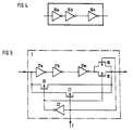
- FIG. 4 shows an example of a delay element corresponding to the delay elements 9 and 10 shown in FIG. 2.
- These can consist of a large number n of inverting or non-inverting driver stages 16a, 16b ... 16n.
- the number of inverting or non-inverting driver stages is immaterial, it is only important that both delay elements 9 and 10 have the same number of driver stages.
- the controllable delay circuit shown in FIG. 5 also has a plurality m of inverting driver stages 17a, 17b ... 17m connected in series.
- the input signal is fed to the input of the first driver stage 17a.
- the input signal reaches the output via the load path of a p-channel FET 20 and via the load path of an n-channel FET 21 connected in parallel.
- the output of the last driver stage 17m is also connected to the output of the controllable delay circuit via the load path of an n-channel FET 19 and via the load path of a p-channel FET 18 connected in parallel to the load path of the FET 19.
- the control input is connected to the gate connection of the n-channel FET 21 and the p-channel FET 18.
- an inverting driver stage 22 is provided, the input of which is also connected to the control input.
- the output of the inverting driver stage 22 is connected both to the gate connection of the p-channel FET 20 and to the gate connection of the n-channel FET 19.
- the digitally controllable delay circuit 3 can be set to different delay times via the discriminator circuit 6. If the runtime discriminator circuit is designed according to FIG. 3, after a disk test the connection 14, which can be separated electrically or by laser, can be opened whenever the measured time parameters make it necessary to correct the holding time.
- the resistor 13 can be replaced by any other component that limits the electrical current flow, e.g. one or more transistors. Of course, other simple logic arrangements containing connections that are electrically or laser-separable are also conceivable.
- the runtime discriminator according to FIG. 2 essentially consists of the two delay elements, which are of different construction but have the same basic runtime under nominal conditions. The delay times fluctuate depending on the manufacturing-related process fluctuations. Any periodic or non-periodic cycle, as may be present in digital integrated circuits, is suitable for controlling the delay elements 9, 10. Since it only has an auxiliary function, its exact shape, location, length, etc. is not decisive.
- the runtime elements 9, 10 are now designed, for example, as shown in FIG. 4, so that process fluctuations have different effects on their runtimes.
- the delay element 9 now experiences a greater delay than the delay element 10
- the D flip-flop 11 now supplies a logic one signal at the output Q and ensures in the controllable delay circuit that the shorter delay time is activated. This counteracts the loss of speed.
- the digitally controllable delay circuit in this case has two different data paths that have different delay times.
- the data path can be switched from one route to the other via appropriate logic.
- the runtime of the first data path should be as short as possible and close to zero in order to avoid problems with the signal delay time in the case of slow circuits.
- the runtime discriminator circuit is designed appropriately, several switchable data paths with different runtimes could also be provided in the controllable delay circuit 3.
- the delay discriminator circuit containing the circuit parts 9, 10, 11 can be constructed centrally, while a digitally controllable delay line is required separately for each output data path.
- the circuit arrangement according to the invention makes it possible to guarantee user-friendly holding times and to allow greater measurement and process tolerances without significantly worsening the overall delay times.
- FIG. 5 shows a simple embodiment for a controllable delay circuit with two data paths of different run times. If a logic zero signal is present at the control input, the FETs 20, 21 are blocked and the FETs 18 and 19 are switched to the conductive state. This results in the data path which takes place via the m-inverter stages 17a, 17b ... 17m and the load paths of the two FETs 18 and 19. If, on the other hand, there is a logic one signal at control input 7, the FETs 18 and 19 are blocked. As a result, the data path between the input and output of the delay circuit is short-circuited via the FETs 20 and 21, and thus a delay time that is close to zero is established.
Landscapes
- Physics & Mathematics (AREA)
- Nonlinear Science (AREA)
- Pulse Circuits (AREA)
Priority Applications (1)
| Application Number | Priority Date | Filing Date | Title |
|---|---|---|---|
| EP92112607A EP0579855A1 (fr) | 1992-07-23 | 1992-07-23 | Circuit de compensation de temps de propagation |
Applications Claiming Priority (1)
| Application Number | Priority Date | Filing Date | Title |
|---|---|---|---|
| EP92112607A EP0579855A1 (fr) | 1992-07-23 | 1992-07-23 | Circuit de compensation de temps de propagation |
Publications (1)
| Publication Number | Publication Date |
|---|---|
| EP0579855A1 true EP0579855A1 (fr) | 1994-01-26 |
Family
ID=8209837
Family Applications (1)
| Application Number | Title | Priority Date | Filing Date |
|---|---|---|---|
| EP92112607A Withdrawn EP0579855A1 (fr) | 1992-07-23 | 1992-07-23 | Circuit de compensation de temps de propagation |
Country Status (1)
| Country | Link |
|---|---|
| EP (1) | EP0579855A1 (fr) |
Cited By (1)
| Publication number | Priority date | Publication date | Assignee | Title |
|---|---|---|---|---|
| WO1997042707A1 (fr) * | 1996-05-06 | 1997-11-13 | Siemens Aktiengesellschaft | Generateur de signal d'horloge |
Citations (9)
| Publication number | Priority date | Publication date | Assignee | Title |
|---|---|---|---|---|
| EP0181047A2 (fr) * | 1984-11-09 | 1986-05-14 | Lsi Logic Corporation | Circuit de commande de retard et méthode pour commander les retards dans un élément semi-conducteur |
| JPS635615A (ja) * | 1986-06-26 | 1988-01-11 | Matsushita Electric Ind Co Ltd | 信号遅延装置 |
| JPH01225220A (ja) * | 1988-03-03 | 1989-09-08 | Nec Corp | 遅延回路 |
| JPH02119312A (ja) * | 1988-10-27 | 1990-05-07 | Nec Corp | 遅延回路 |
| JPH02130020A (ja) * | 1988-11-10 | 1990-05-18 | Nec Corp | 遅延回路 |
| JPH02183622A (ja) * | 1989-01-09 | 1990-07-18 | Sharp Corp | 半導体集積回路 |
| JPH0349417A (ja) * | 1989-07-18 | 1991-03-04 | Nec Corp | 半導体集積回路 |
| JPH03175720A (ja) * | 1989-12-04 | 1991-07-30 | Nec Corp | 半導体集積回路 |
| JPH03261216A (ja) * | 1990-03-09 | 1991-11-21 | Fujitsu Ltd | タイミング可変回路 |
-
1992
- 1992-07-23 EP EP92112607A patent/EP0579855A1/fr not_active Withdrawn
Patent Citations (9)
| Publication number | Priority date | Publication date | Assignee | Title |
|---|---|---|---|---|
| EP0181047A2 (fr) * | 1984-11-09 | 1986-05-14 | Lsi Logic Corporation | Circuit de commande de retard et méthode pour commander les retards dans un élément semi-conducteur |
| JPS635615A (ja) * | 1986-06-26 | 1988-01-11 | Matsushita Electric Ind Co Ltd | 信号遅延装置 |
| JPH01225220A (ja) * | 1988-03-03 | 1989-09-08 | Nec Corp | 遅延回路 |
| JPH02119312A (ja) * | 1988-10-27 | 1990-05-07 | Nec Corp | 遅延回路 |
| JPH02130020A (ja) * | 1988-11-10 | 1990-05-18 | Nec Corp | 遅延回路 |
| JPH02183622A (ja) * | 1989-01-09 | 1990-07-18 | Sharp Corp | 半導体集積回路 |
| JPH0349417A (ja) * | 1989-07-18 | 1991-03-04 | Nec Corp | 半導体集積回路 |
| JPH03175720A (ja) * | 1989-12-04 | 1991-07-30 | Nec Corp | 半導体集積回路 |
| JPH03261216A (ja) * | 1990-03-09 | 1991-11-21 | Fujitsu Ltd | タイミング可変回路 |
Non-Patent Citations (9)
| Title |
|---|
| IBM TECHNICAL DISCLOSURE BULLETIN Band 32, Nr. 1, Juni 1989, Seiten 158,159, Armonk, NY, US; "New Delay-time Tunable Design with Laser-Blown Fuses" * |
| PATENT ABSTRACTS OF JAPAN Band 014, Nr. 455 (E-985), 28. September 1990; & JP - A - 2183622 (SHARP CORP) 18.07.1990 * |
| PATENT ABSTRACTS OF JAPAN Band 12, Nr. 207 (E-621)(3054), 14. Juni 1988; & JP - A - 63 5615 (MATSUSHITA ELECTRIC IND CO LTD) 11.01.1988 * |
| PATENT ABSTRACTS OF JAPAN Band 13, Nr. 544 (E-855)(3892), 6. Dezember 1989; & JP - A - 1225220 (NEC CORP) 08.09.1989 * |
| PATENT ABSTRACTS OF JAPAN Band 14, Nr. 346 (E-956)(4289), 26. Juli 1990; & JP - A - 2119312 (NEC CORP) 07.05.1990 * |
| PATENT ABSTRACTS OF JAPAN Band 14, Nr. 365 (E-961)(4308), 8. August 1990; & JP - A - 2130020 (NEC CORP) 18.05.1990 * |
| PATENT ABSTRACTS OF JAPAN Band 15, Nr. 191 (E-1068), 16. Mai 1991; & JP - A - 3049417 (NEC CORP) 04.04.1991 * |
| PATENT ABSTRACTS OF JAPAN Band 15, Nr. 419 (E-1126), 24. Oktober 1991; & JP - A - 3175720 (NEC CORP) 30.07.1991 * |
| PATENT ABSTRACTS OF JAPAN Band 16, Nr. 67 (E-1168), 19. Februar 1992; & JP - A - 3261216 (FUJITSU LTD) 21.11.1991 * |
Cited By (2)
| Publication number | Priority date | Publication date | Assignee | Title |
|---|---|---|---|---|
| WO1997042707A1 (fr) * | 1996-05-06 | 1997-11-13 | Siemens Aktiengesellschaft | Generateur de signal d'horloge |
| US5986491A (en) * | 1996-05-06 | 1999-11-16 | Siemens Aktiengesellschaft | Clock signal generator |
Similar Documents
| Publication | Publication Date | Title |
|---|---|---|
| DE69231491T2 (de) | Steuerbarer Busabschluss | |
| DE19624270C2 (de) | Komplementärtaktgenerator zum Erzeugen von Komplementärtakten | |
| DE69420476T2 (de) | Verriegelungsgesteuerter Ausgangstreiber | |
| DE68912617T2 (de) | Spannungsseitige MOS-Treiberschaltung. | |
| DE3327260A1 (de) | Schmitt-trigger | |
| DE1762866A1 (de) | Logikschaltung | |
| EP0282981A2 (fr) | Circuit d'attaque numérique en push-pull | |
| DE69029489T2 (de) | Abgleichschaltungen | |
| DE69226746T2 (de) | H-förmige Brückenschaltung mit Schutz vor Kurzschluss während der Stromrichtungsumkehr in der Last | |
| DE102007009848B4 (de) | Ansteuerschaltung | |
| EP0663726A2 (fr) | Circuit d'attaque de sortie | |
| DE3850808T2 (de) | Erzeugung von Taktimpulsen. | |
| DE10255642B4 (de) | Verfahren und Vorrichtung zum Ausgeben eines Digitalsignals | |
| DE68925856T2 (de) | Logische Bicmos-Schaltung | |
| DE19700045A1 (de) | CMOS-Ausgangspuffer mit hoher Stromsteuerfähgikeit bei niedrigem Rauschen | |
| DE102004050464B4 (de) | Ausgangsschaltung | |
| DE4430049C1 (de) | Schaltungsanordnung zur Unterspannungs-Erkennung | |
| DE4324138B4 (de) | CMOS-Drei-Zustands-Pufferschaltung | |
| EP0778673A1 (fr) | Circuit intégré avec circuit d'attaque de sortie programmable | |
| DE69416554T2 (de) | Ringoszillatorschaltung für spannungsgesteuerten Oszillator mit frequenzunabhängigem Tastverhältnis | |
| EP0203535B1 (fr) | Méthode pour la simulation d'une erreur dans un circuit logique et dispositif pour la réalisation d'une telle méthode | |
| DE10143432C1 (de) | Treiberschaltung und Ansteuerverfahren für einen feldgesteuerten Leistungsschalter | |
| EP0961291A1 (fr) | Circuit de verrouillage à fusible | |
| DE3318957A1 (de) | Monolithisch integrierbare, bistabile multivibratorschaltung mit einem in einen vorzugszustand einstellbaren ausgang | |
| DE3781543T2 (de) | Unterdrueckungsschaltung von unerwuenschten zeitlichen abschnitten eines variablen spannungssignals. |
Legal Events
| Date | Code | Title | Description |
|---|---|---|---|
| PUAI | Public reference made under article 153(3) epc to a published international application that has entered the european phase |
Free format text: ORIGINAL CODE: 0009012 |
|
| AK | Designated contracting states |
Kind code of ref document: A1 Designated state(s): AT BE CH DE DK ES FR GB GR IT LI LU MC NL PT SE |
|
| RBV | Designated contracting states (corrected) |
Designated state(s): DE |
|
| STAA | Information on the status of an ep patent application or granted ep patent |
Free format text: STATUS: THE APPLICATION IS DEEMED TO BE WITHDRAWN |
|
| 18D | Application deemed to be withdrawn |
Effective date: 19940727 |