EP0579922A1 - Dispositif de transmission de données pour un réseau local - Google Patents
Dispositif de transmission de données pour un réseau local Download PDFInfo
- Publication number
- EP0579922A1 EP0579922A1 EP93108149A EP93108149A EP0579922A1 EP 0579922 A1 EP0579922 A1 EP 0579922A1 EP 93108149 A EP93108149 A EP 93108149A EP 93108149 A EP93108149 A EP 93108149A EP 0579922 A1 EP0579922 A1 EP 0579922A1
- Authority
- EP
- European Patent Office
- Prior art keywords
- input
- output
- signal
- network
- pole
- Prior art date
- Legal status (The legal status is an assumption and is not a legal conclusion. Google has not performed a legal analysis and makes no representation as to the accuracy of the status listed.)
- Granted
Links
Images

Classifications
-
- H—ELECTRICITY
- H04—ELECTRIC COMMUNICATION TECHNIQUE
- H04L—TRANSMISSION OF DIGITAL INFORMATION, e.g. TELEGRAPHIC COMMUNICATION
- H04L12/00—Data switching networks
- H04L12/28—Data switching networks characterised by path configuration, e.g. LAN [Local Area Networks] or WAN [Wide Area Networks]
- H04L12/44—Star or tree networks
-
- H—ELECTRICITY
- H04—ELECTRIC COMMUNICATION TECHNIQUE
- H04L—TRANSMISSION OF DIGITAL INFORMATION, e.g. TELEGRAPHIC COMMUNICATION
- H04L12/00—Data switching networks
- H04L12/28—Data switching networks characterised by path configuration, e.g. LAN [Local Area Networks] or WAN [Wide Area Networks]
- H04L12/40—Bus networks
-
- H—ELECTRICITY
- H04—ELECTRIC COMMUNICATION TECHNIQUE
- H04L—TRANSMISSION OF DIGITAL INFORMATION, e.g. TELEGRAPHIC COMMUNICATION
- H04L25/00—Baseband systems
- H04L25/38—Synchronous or start-stop systems, e.g. for Baudot code
- H04L25/40—Transmitting circuits; Receiving circuits
- H04L25/49—Transmitting circuits; Receiving circuits using code conversion at the transmitter; using predistortion; using insertion of idle bits for obtaining a desired frequency spectrum; using three or more amplitude levels ; Baseband coding techniques specific to data transmission systems
- H04L25/4917—Transmitting circuits; Receiving circuits using code conversion at the transmitter; using predistortion; using insertion of idle bits for obtaining a desired frequency spectrum; using three or more amplitude levels ; Baseband coding techniques specific to data transmission systems using multilevel codes
- H04L25/4923—Transmitting circuits; Receiving circuits using code conversion at the transmitter; using predistortion; using insertion of idle bits for obtaining a desired frequency spectrum; using three or more amplitude levels ; Baseband coding techniques specific to data transmission systems using multilevel codes using ternary codes
- H04L25/4925—Transmitting circuits; Receiving circuits using code conversion at the transmitter; using predistortion; using insertion of idle bits for obtaining a desired frequency spectrum; using three or more amplitude levels ; Baseband coding techniques specific to data transmission systems using multilevel codes using ternary codes using balanced bipolar ternary codes
Definitions
- the invention relates to a data transmission arrangement for a local data network of the type mentioned in the preamble of claim 1.
- Such data transmission arrangements are advantageously used in a local data network which works with an asynchronous data transmission protocol, which is constructed from individual UART characters (bit-serial character).
- AMI coding alternative mark inversion
- An AMI coding device is known (DE 37 35 395 C2), in which an arithmetic unit is used for coding.
- a serial transmission and reception unit is known (GB 22 38 931 A), which uses a transformer with a center tap to couple a network node to a transmission cable of a data network.
- the invention has for its object to provide a reliable data transmission arrangement for a local data network with a changeable tree-shaped topology, which enables the construction of an inexpensive network driver unit for a network node.
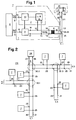
- 1 means a network driver unit, in which a code generator 2, a decoding unit 3 and a coupling element 4 for a transmission medium 5 are arranged.
- the network driver unit 1 and a serial transmission / reception unit 6 are parts of a network node 7.
- the transmitting / receiving unit 6 has an output 8 for bit-serial data TxD and an input 9 for bit-serial data RxD and is advantageously a serial communication unit (serial communication interface SCI) of a microcomputer or a UART (universal asynchronous receiver / transmitter).
- serial communication unit serial communication interface SCI
- the code generator 2 has a coding unit 10 and a constant current stage 11 connected to the coding unit 10 with a first output pole 12 for a current i and a second output pole 13 for the current i.
- An input 14 of the coding unit 10 is connected to the output 8 of the transmission / reception unit 6.
- the decoding unit 3 has an output 15 connected to the input 9 of the transmitting / receiving unit and two input poles 16 and 17, of which a first input pole 16 with the first output pole 12 of the constant current stage 11 and a first input pole 18 of the coupling element 4 is connected, while the second input pole 17 is connected to the second output pole 13 of the constant current stage 11 and to a second input pole 19 of the coupling element 4.
- the transmission medium 5 consists of at least one cable harness 5.1, which has at least two wires, of which a first wire 20 with a first connection pole 22 of the coupling element 4 and also a first connection 23 of a network termination 24 and a second wire 21 with a second connection pole 25 of the coupling element 4 and a second connection 26 of the network termination 24 is connected.
- the network termination 24 is advantageously a series circuit consisting of an ohmic resistor 27 and a capacitor 28.
- the capacitor 28 separates the resistor 27 from the transmission medium 5 in terms of direct current.
- seven network nodes 7 of a local data network 29 are connected to the transmission medium 5 consisting of a number s of cable strands, which has the network termination 24 on a first cable strand 5.1.
- the network termination 24 can in principle be placed at any point on the transmission medium 5.
- the number s is basically not limited and is four in the data network 29 shown.
- cable branches 30 designated 30.1 to 30.4 in FIG. 2
- two cable strands are connected to one another in such a way that the topology of the data network 29 is in principle tree-shaped, the tree being fundamentally branched and thus degenerate.
- Each wire 20 or 21 of the first cable harness 5.1 is connected to a first wire branch 30.1 with one wire 20 or 21 of a second wire harness 5.2 and to a second wire junction 30.2 with one wire 20 or 21 of a third wire harness 5.3. Furthermore, one wire 20 or 21 of the third cable harness 5.3 is connected to a third wire branch 30.3 with one wire 20 or 21 of a fourth wire harness 5.4.
- the maximum k of the number of connected network nodes 7 is fundamentally not restricted. In favor of an acceptable maximum response time for a token passing method and also in order to achieve a small address range, the maximum k is advantageously limited to 127.
- the sum of the lengths of all the cable strands 5.1, 5.2, 5.3, 5.4 is limited to about 1000 m in favor of a further advantage, namely not to use line amplifiers (repeaters). If required, data networks 29 are coupled for larger expansions in a known manner via line amplifiers.
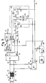
- An advantageous embodiment of the network driver unit 1 with the coupling element 4 and the bipolar constant current stage 11 shown in FIG. 3 has one via two signal inputs and a first output (31) for a signal Pos and a second output (32) for one Comparator circuit 33 having signal neg, a signal filter 38 constructed from an OR gate 36 and a dual up / down counter 37, a polarity detector 39 with an output 40 for a signal RP, one from a flip-flop 41, an exclusive OR gate 42 and a first frequency divider 43 constructed generator part 44 and a quartz oscillator 45 with a second frequency divider 46 (prescaler) connected downstream of the quartz oscillator 45.
- the first input pole 16 is a first signal input of the comparator circuit 33, while the second input pole 17 is realized by the second signal input of the comparator circuit 33.
- Comparator circuit 33 has its first output 31 connected to a first input 51 of OR gate 36 and a first control input 52 of polarity detector 39, while second output 32 is connected to a second input 53 of OR gate 36 and to a second one Control input 54 of the polarity detector 39 is connected.
- a control input 55 for a control signal IN of the up / down counter 37 is connected to an output 56 of the OR gate 36.
- the output 15 of the decoding unit 3 (FIG. 1) is an output of the up / down counter 37 and at the same time also an output of the signal filter 38.
- the output 40 of the polarity detector 39 is connected to a data input 57 of the flip-flop 41, which with The advantage is a D flip-flop (data latch) which can be triggered at a clock input 58 with a negative or falling edge and has a data output 59, the data input 57 being the D input of the D flip-flop.
- the data output 59 for a signal pole of the flip-flop 41 is connected to a first input 60 of the exclusive-OR gate 42, from which a second input 61 is connected to an output 62 for a signal TB of the first frequency divider 43.
- the bipolar constant current stage 11 has a first control input 64 for an control signal TP connected to an output 63 of the exclusive-OR gate 42 and a second control input 65 for the bit-serial data TxD connected to the input 14 of the network driver unit 1. Furthermore, the input 14 leads to the clock input 58 of the flip-flop 41 as well as to a reset input 66 of the first frequency divider 43 and to a reset input 67 of the second frequency divider 46.
- An output 68 of the second frequency divider 46 intended for an advantageously binary clock signal CLK leads to a clock input 69 of the up / down counter 37, to a clock input 70 of the polarity detector 39 and to a clock input 71 of the first frequency divider 43.
- the coupling element 4 advantageously has a transformer 74 and a capacitor 75 provided with a first winding 72 and a second winding 73, the two input poles 18 and 19 being the connections of the first winding 72 and one between the two connection poles 22 and 25 the capacitor 75 and the second winding 73 existing series connection.
- the capacitor 75 decouples the transformer 74 in direct current from the transmission medium 5.
- the comparator circuit 33 is advantageously designed such that common mode noise, which essentially occurs as a result of the capacitance of the transformer 74, is effectively suppressed.
- a voltage limiting element is connected between the two connection poles 22 and 25, in parallel to the series circuit consisting of the capacitor 75 and the second winding 73.
- An asynchronous data transmission protocol of a higher layer (upper layer) of the data transmission network 29 is constructed from protocol characters - for example from ASCII characters (american standard code for information interchange) - which are located in the network node 7 between the transmitting / receiving unit (6) and the network driver unit (1) in the form of the bit serial data TxD or RxD are exchanged.
- the protocol characters of the bit serial data TxD or RxD have a constant length, that is to say that a number n of bits per protocol character of the data transmission protocol is constant.
- each protocol character of the bit-serial data TxD or RxD has a number of n 1 start bits, a number of n 2 actual information bits, a number of n 3 test bits and a number of n stop bits.
- the number n1 and the number n2, the number n3 and the number n4 advantageously corresponds to a known standard, which also specifies a sequence of the individual bits of the protocol characters.
- Each protocol character of the bit serial data TxD or RxD advantageously has an even number of bits with the value "0” or then an even number of bits with the value "1", so that with a low circuitry complexity, a signal can be generated from a log character which has the value zero averaged over the duration of the log character.
- n bits of the protocol character are in the network node 7 between the network driver unit (1) and the transmit / receive unit 6 and also between the network nodes 7 of the data network 29 with a stable bit rate f bit , that is within the Protocol character transmitted bit-synchronously.
- the code generator 2 shown in FIG. 1 transforms each protocol character of the bit serial data TxD into a ternary code, which is advantageously shown as a substantially constant current i in sections in the two output poles 12 and 13.
- the value of the current i averaged over the duration of a log character is advantageously zero.
- the amount of current i is advantageously substantially constant during the pulse time T bit .
- the binary value which is always present in an even number in the protocol character is advantageously transmitted as an impulse in the AMI code, the polarity of a subsequent impulse always being reversed compared to its preceding impulse.
- the current i flows essentially through the input poles 18 and 19 of the coupling element 4, which tansforms the pulses of the current i into corresponding pulses of a voltage lying between the two connection poles 22 and 25 u22 ⁇ 25.
- the constant current stage 11 brings against a voltage stage the advantages that resonance phenomena of a resonant circuit formed essentially from the transformed capacity of the transmission medium 5 and the leakage inductance of the transformer 74 are effectively prevented and that the voltage u22 ⁇ 25 on the transmission medium 5 increases with distance from the network termination 24 due to the line resistance of the transmission medium 5 increased.
- An input impedance of the coupling element 4 acting between the two input poles 18 and 19 is advantageously at least about 1000 times smaller than the input impedance of the decoding unit 3 acting between the input poles 16 and 17.
- the decoding unit 3 converts a voltage corresponding to the AMI-coded protocol character, lying between the two input poles 16 and 17, into the bit-serial data RxD of the protocol character.
- the decoding unit 3 works simultaneously with the code generator 3 and transmits the coding unit 10 the polarity of a previously registered pulse of the voltage u18 ⁇ 19.
- An AC voltage lying between the two wires 20 and 21 of the transmission medium 5 is transmitted in the network node 7 through the coupling element 4 at its two input poles 18 and 19 to the input poles 16 and 17 of the decoding unit 3.
- the coupling element 4 essentially fulfills four tasks, namely the transmission of the code generated by the code generator 2 in the form of a current i from the network node 7 to the transmission medium 5, the transmission of a code in the form of a voltage u22 ⁇ 25 from the transmission medium 5 to the decoding unit 3 of the network node, a direct current decoupling of the network node 7 from the transmission medium and an electrical isolation of the network node 7 from the transmission medium 5 and thus an electrical isolation of all Network node 7 of the data network 29.
- the essential parameters of the coupling element 4, the transmission medium 5 and the network termination 24 are matched to one another in a known manner at the desired bit rate f bit .
- Fig. 4 shows a positive pulse of length T bit of the current i and the advantageous step response of the voltage u22 ⁇ 25 on the positive edge of the pulse. Delayed by a time of at most 0.35 ⁇ T bit on the positive edge, the voltage u22525 runs within a rectangular window 77. The voltage u22 ⁇ 25 in window 77 deviates at most 15% from its nominal value at logic "1". The window 77 limits the guaranteed course of the advantageous step response.
- the protocol characters of the bit serial data TxD or RxD are required for this version in accordance with a UART character used in the DIN 19 245 standard (Process Field Bus, PROFIBus), which has a start bit with the value "0", eight information bits in the order listed , has a check bit and a stop bit with the value "1".
- the check bit is a parity bit which, by its value, defines a sum of the bits whose value is "1" to an even value, the information bits and the check bit of the protocol character being taken into account to form the sum.
- the network driver unit 1 can be adapted for other protocol characters after simple considerations.
- An AMI code is coded or decoded in the network driver unit 1, in which the value "0" of the protocol character is represented as a pulse.
- the protocol character has an even number of bits with the value "0” and the bit serial data TxD and RxD have the value "1" between two protocol characters (in the so-called idle state).
- FIG. 5 A basic course of signals in Fig. 5 exemplifies essential steps in the decoding of the AMI code of the voltage u1 u18 ⁇ .
- the time unit T corresponds to the pulse time T bit and has a duration of 52 ⁇ s, for example at a bit rate f bit of 19200 s ⁇ 1.
- the frequency f CLK of the clock signal CLK is a multiple of the bit rate f bit .
- the clock signal CLK advantageously has the frequency f CLK of 614.4 kHz.
- the binary signal Pos (Fig. 5b) at the first output 31 of the comparator circuit 33 is only in the case of a positive pulse of the voltage u18 ⁇ 19 to "1", while the binary signal Neg (Fig. 5c) at the second output 32 of the comparator circuit 33rd with a negative pulse of the voltage u18 ⁇ 19 to logic "1".
- the binary signal RP (Fig. 5e) at the output 40 of the polarity detector 39 represents the current polarity of the pulses of the voltage u18 ⁇ 19 largely without interference; with logic "1" a positive pulse, with logic "0" a negative pulse.
- the polarity detector 39 is an up / down counter with a counter Z39 (Fig. 5d), which can be changed between zero and an upper value b by means of pulses of the clock signal CLK.
- the value b determines the interference immunity of the polarity detector 39.
- the signal IN (Fig. 5f) is formed from the two signals Pos and Neg, has the course (Pos OR Neg) and controls the counting direction of the up / down counter 37 whose count Z37 (Fig. 5g) by means of pulses of the clock signal CLK is changeable between zero and an upper value d. If the signal IN is logic "1" and the counter reading Z37 is less than the value d, a pulse of the clock signal CLK increases the counter reading Z37 by one when the signal IN is logic "0" and the counter reading Z37 is greater than zero a pulse of the clock signal CLK the counter Z37 by one. When the counter reading Z37 reaches the value d, the signal ⁇ RxD inverse to the bit serial data RxD (Fig. 5h) becomes logic "1" and keeps the value until the counter reading Z39 reaches zero, whereupon the signal ⁇ RxD turns to logic "0" changes.
- the signal IN is formed and used when decoding the AMI code, which in principle represents "pulse of the AMI code” and "no pulse of the AMI code"
- the positive and negative pulses of the voltage u18 ⁇ 19 are basically in decoding equal, whereby the two connection poles 22 and 25 of the network driver unit 1 can be interchanged without loss of function, which is advantageous when connecting the network node 7.
- the value d determines the effect of the signal filter 38.
- a first arrow denotes the start bit of the bit serial data RxD and further arrows indicate the times at which the data RxD are scanned in the transmission / reception unit 6.
- the current information value of the bit serial data RxD is indicated by the arrows.
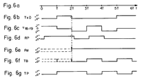
- FIG. 6 A basic course of signals in Fig. 6 explains examples of essential steps in the coding of the AMI code of the current i or the voltage u18 ⁇ 19 (Fig. 6c) from the bit serial data TxD (Fig. 6b).
- the time unit T corresponds to the pulse time T bit and has a duration of 52 ⁇ s, for example at a bit rate f bit of 19200 s ⁇ 1.
- the binary signal RP (Fig. 6d and Fig. 5e) represents the polarity of the last determined pulse of the voltage u18 ⁇ 19, which determines the polarity of the subsequent pulse in the AMI code.
- the fact that the coding depends on the polarity of the last determined pulse of the voltage u18 ⁇ 19 ensures that successive pulses of the voltage u18 ⁇ 19 always have different polarity, so that the transformer 74 is also driven symmetrically when the mains Driver unit 1 alternates between receiving and sending.
- the flip-flop 41 causes the binary signal Pol (FIG. 6e) to have the instantaneous value of the signal RP at the time of the negative edge after a negative edge of the signal TxD.
- the division is restarted by a negative edge at the reset input 66.
- the pulse time of the signal TB is advantageously the same as its pause time.
- the control signal TP (FIG. 6g) is formed from the two signals Pol and TB and has the shape (Pol XOR TB), where XOR means the Boolean antivalence.
- the polarity of the current i is determined in the constant current stage 11 by the control signal TP, which ensures that the polarity of subsequent pulses of the current i always changes.
- the control signal TP also ensures that the polarity of a pulse of the current i is reversed from the polarity of a pulse of the voltage u18 ⁇ 19 last preceding this current pulse.
- the constant current stage 11 selects the polarity of the current (i) based on the control signal TP such that successive pulses of the voltage (u18 ⁇ 18 ⁇ ) between the two input poles (18; 19) have a different polarity.
- the constant current stage 11 essentially consists, for example, of a constant current source that can be switched off and four controllable switches connected to form an H bridge.
- the second frequency divider 46 with a division q2 forms the clock signal CLK from the output signal of the crystal oscillator 45.
- the division is restarted by a negative edge at the reset input 67.
- the cable strands of the transmission medium are advantageously conventional twisted pair cables.
- the steepness of the step response of the voltage u22 ⁇ 25 (FIG. 4) and thus the limits of the window 77 are due to the leakage inductance L S of the transformer 74 (FIG. 3) which can be determined with the short-circuited second winding 73, through the ohmic resistor 27 (FIG. 1) of the network termination 24 and can be influenced by a supply voltage available from the constant current stage 11 (FIG. 3) for generating a pulse of the current i.
- the constant current stage 11 enables the advantageous increase in the step response in a simple manner.
- the advantageous step response results when the resistor 27 has a nominal value of 100 ohms and the leakage inductance L s is between 0.75 mH and 2.25 mH.
- the two windings 72 and 73 advantageously have the same inductance L, which is advantageously greater than 1.5 H.
- the transmission medium 5 is advantageously terminated at all times by the network termination 24, so that the transformer 74 does not cause any interference pulses on the transmission medium 5 due to its inductance, in particular when transitioning from a transmission to a transmission pause.
- the two wires 20 and 21 can additionally transmit one Serve DC voltage with which the network nodes 7 can be fed via the transmission medium 5 with little effort.
- the network driver unit 1 which contains the decoding unit 3, the code generator 2 with the constant current stage 11 and the coupling element 4 with the transformer 74 has, the topology of the data network 29 can be changed by simple means within wide limits with a small risk of interference.
- the network driver unit 1 is reliable and inexpensive to manufacture.
Landscapes
- Engineering & Computer Science (AREA)
- Computer Networks & Wireless Communication (AREA)
- Signal Processing (AREA)
- Physics & Mathematics (AREA)
- Spectroscopy & Molecular Physics (AREA)
- Dc Digital Transmission (AREA)
Applications Claiming Priority (2)
| Application Number | Priority Date | Filing Date | Title |
|---|---|---|---|
| CH221792 | 1992-07-14 | ||
| CH2217/92 | 1992-07-14 |
Publications (2)
| Publication Number | Publication Date |
|---|---|
| EP0579922A1 true EP0579922A1 (fr) | 1994-01-26 |
| EP0579922B1 EP0579922B1 (fr) | 1998-03-11 |
Family
ID=4228595
Family Applications (1)
| Application Number | Title | Priority Date | Filing Date |
|---|---|---|---|
| EP19930108149 Expired - Lifetime EP0579922B1 (fr) | 1992-07-14 | 1993-05-19 | Dispositif de transmission de données pour un réseau local |
Country Status (2)
| Country | Link |
|---|---|
| EP (1) | EP0579922B1 (fr) |
| DE (1) | DE59308239D1 (fr) |
Citations (2)
| Publication number | Priority date | Publication date | Assignee | Title |
|---|---|---|---|---|
| FR2567702A1 (fr) * | 1984-07-13 | 1986-01-17 | France Etat | Emetteur a courant constant pour la transmission de donnees sur une ligne de transmission |
| EP0316536A2 (fr) * | 1987-11-13 | 1989-05-24 | Mitsubishi Denki Kabushiki Kaisha | Poste terminal dans un système de transmission d'information |
-
1993
- 1993-05-19 EP EP19930108149 patent/EP0579922B1/fr not_active Expired - Lifetime
- 1993-05-19 DE DE59308239T patent/DE59308239D1/de not_active Expired - Fee Related
Patent Citations (2)
| Publication number | Priority date | Publication date | Assignee | Title |
|---|---|---|---|---|
| FR2567702A1 (fr) * | 1984-07-13 | 1986-01-17 | France Etat | Emetteur a courant constant pour la transmission de donnees sur une ligne de transmission |
| EP0316536A2 (fr) * | 1987-11-13 | 1989-05-24 | Mitsubishi Denki Kabushiki Kaisha | Poste terminal dans un système de transmission d'information |
Non-Patent Citations (1)
| Title |
|---|
| IEEE TRANSACTIONS ON COMMUNICATIONS Bd. 33, Nr. 5, Mai 1985, NEW YORK US Seiten 470 - 478 H. T. MOUFTAH ET AL. 'Design and Performance Study of a Microprocessor-Based Two-Wire full Duplex Baseband Modem' * |
Also Published As
| Publication number | Publication date |
|---|---|
| EP0579922B1 (fr) | 1998-03-11 |
| DE59308239D1 (de) | 1998-04-16 |
Similar Documents
| Publication | Publication Date | Title |
|---|---|---|
| DE3788538T2 (de) | Kollisionsdetektionstechnik für ein passives, optisches, lokales Sternnetz mit CSMA/CD. | |
| DE3586627T2 (de) | Digitale integrierte mehrzweckschaltung fuer uebertragungs- und steuernetzwerk. | |
| DE69533237T2 (de) | Vorrichtung zum senden und/oder empfangen von daten mit verschiedenen datenübertragungsraten | |
| DE19742043A1 (de) | Vorrichtung zur Übertragung digitaler Daten mit mehreren Datentransferraten | |
| DE2417124A1 (de) | Methode zur datenuebertragung und system zur anwendung dieser methode | |
| DE1154831B (de) | Anordnung zur Regenerierung einer ein Taktsignal enthaltenden bipolaren Impulsfolge unter Verwendung von Impulsuebertragungsverfahren nach Art der Pulskodemodulation | |
| DE2901235A1 (de) | Digitales zweidraht-vollduplex- uebertragungssystem | |
| EP0168770A2 (fr) | Bus pour données optiques utilisant une méthode d'accès statistique | |
| DE3851969T2 (de) | Empfangskoppler für Übertragungssysteme von Binärdaten. | |
| EP0115327B1 (fr) | Décodeur CMI | |
| DE3204227A1 (de) | Digitale fernmeldeendstelle zur uebertragung von informationen zu einer digitalen fernmeldeanlage, insbesondere zu einer fernsprechanlage bzw. fernsprechnebenstellenanlage | |
| EP0111309B1 (fr) | Décodeur CMI | |
| DE3341904A1 (de) | Verfahren und vorrichtung zur asynchronen datenuebertragung | |
| DE69008917T2 (de) | Einrichtungen mit Frequenzumtastung für Stromschleife. | |
| EP0579922B1 (fr) | Dispositif de transmission de données pour un réseau local | |
| EP0097947B1 (fr) | Dispositif pour générer des séquences pseudo-aléatoires en code AMI | |
| DE2208478B2 (de) | Verfahren und Schaltungsanordnungen zur doppelt gerichteten Datenübertragung über einen Zweidraht-Übertragungskanal | |
| EP0058754B1 (fr) | Dispositif pour l'injection de signaux numériques dans un système filaire | |
| DE4200867C2 (de) | Vorrichtung zur Erkennung einer Codeverletzung | |
| CH648445A5 (de) | Verfahren zur uebertragung binaerer signale ueber ein fremdes drahtnetz. | |
| DE1806905B2 (de) | Impulsformerschaltung | |
| DE1294989B (de) | Verfahren und Schaltungsanordnungen zur digitalen Datenuebertragung | |
| DE69324597T2 (de) | Leitungstreiberschaltung | |
| DE3444361A1 (de) | Datenuebertragungseinrichtung | |
| EP0072393B1 (fr) | Discriminateur de fréquence numérique |
Legal Events
| Date | Code | Title | Description |
|---|---|---|---|
| PUAI | Public reference made under article 153(3) epc to a published international application that has entered the european phase |
Free format text: ORIGINAL CODE: 0009012 |
|
| AK | Designated contracting states |
Kind code of ref document: A1 Designated state(s): BE CH DE FR GB IT LI SE |
|
| 17P | Request for examination filed |
Effective date: 19940222 |
|
| RAP1 | Party data changed (applicant data changed or rights of an application transferred) |
Owner name: LANDIS & GYR TECHNOLOGY INNOVATION AG |
|
| 17Q | First examination report despatched |
Effective date: 19961126 |
|
| GRAG | Despatch of communication of intention to grant |
Free format text: ORIGINAL CODE: EPIDOS AGRA |
|
| GRAG | Despatch of communication of intention to grant |
Free format text: ORIGINAL CODE: EPIDOS AGRA |
|
| GRAH | Despatch of communication of intention to grant a patent |
Free format text: ORIGINAL CODE: EPIDOS IGRA |
|
| GRAH | Despatch of communication of intention to grant a patent |
Free format text: ORIGINAL CODE: EPIDOS IGRA |
|
| GRAA | (expected) grant |
Free format text: ORIGINAL CODE: 0009210 |
|
| AK | Designated contracting states |
Kind code of ref document: B1 Designated state(s): BE CH DE FR GB IT LI SE |
|
| PG25 | Lapsed in a contracting state [announced via postgrant information from national office to epo] |
Ref country code: IT Free format text: LAPSE BECAUSE OF FAILURE TO SUBMIT A TRANSLATION OF THE DESCRIPTION OR TO PAY THE FEE WITHIN THE PRE;WARNING: LAPSES OF ITALIAN PATENTS WITH EFFECTIVE DATE BEFORE 2007 MAY HAVE OCCURRED AT ANY TIME BEFORE 2007. THE CORRECT EFFECTIVE DATE MAY BE DIFFERENT FROM THE ONE RECORDED.SCRIBED TIME-LIMIT Effective date: 19980311 Ref country code: FR Free format text: LAPSE BECAUSE OF FAILURE TO SUBMIT A TRANSLATION OF THE DESCRIPTION OR TO PAY THE FEE WITHIN THE PRESCRIBED TIME-LIMIT Effective date: 19980311 |
|
| REG | Reference to a national code |
Ref country code: CH Ref legal event code: EP |
|
| GBT | Gb: translation of ep patent filed (gb section 77(6)(a)/1977) |
Effective date: 19980312 |
|
| REF | Corresponds to: |
Ref document number: 59308239 Country of ref document: DE Date of ref document: 19980416 |
|
| PG25 | Lapsed in a contracting state [announced via postgrant information from national office to epo] |
Ref country code: LI Free format text: LAPSE BECAUSE OF NON-PAYMENT OF DUE FEES Effective date: 19980531 Ref country code: CH Free format text: LAPSE BECAUSE OF NON-PAYMENT OF DUE FEES Effective date: 19980531 Ref country code: BE Free format text: LAPSE BECAUSE OF NON-PAYMENT OF DUE FEES Effective date: 19980531 |
|
| PG25 | Lapsed in a contracting state [announced via postgrant information from national office to epo] |
Ref country code: SE Free format text: LAPSE BECAUSE OF FAILURE TO SUBMIT A TRANSLATION OF THE DESCRIPTION OR TO PAY THE FEE WITHIN THE PRESCRIBED TIME-LIMIT Effective date: 19980611 Ref country code: GB Free format text: LAPSE BECAUSE OF NON-PAYMENT OF DUE FEES Effective date: 19980611 |
|
| EN | Fr: translation not filed | ||
| BERE | Be: lapsed |
Owner name: LANDIS & GYR TECHNOLOGY INNOVATION A.G. Effective date: 19980531 |
|
| PLBE | No opposition filed within time limit |
Free format text: ORIGINAL CODE: 0009261 |
|
| REG | Reference to a national code |
Ref country code: CH Ref legal event code: PL |
|
| GBPC | Gb: european patent ceased through non-payment of renewal fee |
Effective date: 19980611 |
|
| PG25 | Lapsed in a contracting state [announced via postgrant information from national office to epo] |
Ref country code: DE Free format text: LAPSE BECAUSE OF NON-PAYMENT OF DUE FEES Effective date: 19990302 |
|
| 26N | No opposition filed |