EP0580237A1 - Leistungsfaktorkorrekturschaltung - Google Patents
Leistungsfaktorkorrekturschaltung Download PDFInfo
- Publication number
- EP0580237A1 EP0580237A1 EP93202111A EP93202111A EP0580237A1 EP 0580237 A1 EP0580237 A1 EP 0580237A1 EP 93202111 A EP93202111 A EP 93202111A EP 93202111 A EP93202111 A EP 93202111A EP 0580237 A1 EP0580237 A1 EP 0580237A1
- Authority
- EP
- European Patent Office
- Prior art keywords
- input voltage
- power factor
- semiconductor switch
- factor correction
- correction circuit
- Prior art date
- Legal status (The legal status is an assumption and is not a legal conclusion. Google has not performed a legal analysis and makes no representation as to the accuracy of the status listed.)
- Granted
Links
Images

Classifications
-
- H—ELECTRICITY
- H02—GENERATION; CONVERSION OR DISTRIBUTION OF ELECTRIC POWER
- H02M—APPARATUS FOR CONVERSION BETWEEN AC AND AC, BETWEEN AC AND DC, OR BETWEEN DC AND DC, AND FOR USE WITH MAINS OR SIMILAR POWER SUPPLY SYSTEMS; CONVERSION OF DC OR AC INPUT POWER INTO SURGE OUTPUT POWER; CONTROL OR REGULATION THEREOF
- H02M1/00—Details of apparatus for conversion
- H02M1/42—Circuits or arrangements for compensating for or adjusting power factor in converters or inverters
- H02M1/4208—Arrangements for improving power factor of AC input
- H02M1/4225—Arrangements for improving power factor of AC input using a non-isolated boost converter
-
- Y—GENERAL TAGGING OF NEW TECHNOLOGICAL DEVELOPMENTS; GENERAL TAGGING OF CROSS-SECTIONAL TECHNOLOGIES SPANNING OVER SEVERAL SECTIONS OF THE IPC; TECHNICAL SUBJECTS COVERED BY FORMER USPC CROSS-REFERENCE ART COLLECTIONS [XRACs] AND DIGESTS
- Y02—TECHNOLOGIES OR APPLICATIONS FOR MITIGATION OR ADAPTATION AGAINST CLIMATE CHANGE
- Y02B—CLIMATE CHANGE MITIGATION TECHNOLOGIES RELATED TO BUILDINGS, e.g. HOUSING, HOUSE APPLIANCES OR RELATED END-USER APPLICATIONS
- Y02B70/00—Technologies for an efficient end-user side electric power management and consumption
- Y02B70/10—Technologies improving the efficiency by using switched-mode power supplies [SMPS], i.e. efficient power electronics conversion e.g. power factor correction or reduction of losses in power supplies or efficient standby modes
-
- Y—GENERAL TAGGING OF NEW TECHNOLOGICAL DEVELOPMENTS; GENERAL TAGGING OF CROSS-SECTIONAL TECHNOLOGIES SPANNING OVER SEVERAL SECTIONS OF THE IPC; TECHNICAL SUBJECTS COVERED BY FORMER USPC CROSS-REFERENCE ART COLLECTIONS [XRACs] AND DIGESTS
- Y02—TECHNOLOGIES OR APPLICATIONS FOR MITIGATION OR ADAPTATION AGAINST CLIMATE CHANGE
- Y02P—CLIMATE CHANGE MITIGATION TECHNOLOGIES IN THE PRODUCTION OR PROCESSING OF GOODS
- Y02P80/00—Climate change mitigation technologies for sector-wide applications
- Y02P80/10—Efficient use of energy, e.g. using compressed air or pressurized fluid as energy carrier
Definitions
- the invention relates to a power factor correction circuit.
- a power factor correction circuit serves to correct the poor power factor occurring during rectification and smoothing of the mains voltage, as used in, for instance, switching supplies.
- the known circuits have current programming at the input thereof. As a consequence, higher harmonics may be produced round the zero passages of the input mains voltage due to swing-in phenomena of the input filter.
- a circuit with IC type TDA 4814 has as a further drawback that in the case of a universal mains input for an a.c. voltage of 115 V as well as an a.c. voltage of 230 V, the difference between minimum and maximum operating frequency becomes very great, particularly if also the load varies very strongly. This causes problems of control, efficiency and radiofrequency interference elimination.
- a first object of the invention is to provide a power factor correction circuit which does not need a multiplier, which further has a high efficiency, of the order of magnitude of 98% or more, has no problems with incidental overvoltages at the input, has only very small losses due to reverse recovery currents in the rectifier diode and has a resistance character at the input, so that the input filter is damped automatically.
- the proper operation at an input voltage of 115 V as well as 230 V is optimized, while in other embodiments, as the third and fourth objects respectively, the behavior at a very low load is improved and the capacitive character of the input filter is compensated.
- a fifth object is to permit, in yet another embodiment, a large control amplification, so that the deviations of the output voltage remain small in the event of jumps in the load and the mains voltage, even with a relatively small smoothing capacitor.
- the first object can be realized by providing that, in a power factor correction circuit intended for being connected to a one-phase a.c. mains voltage and comprising a series connection of a self-induction and a controllable power semiconductor, arranged after a rectifier, for instance a bridge rectifier, the junction of the controllable power semiconductor and self-induction being connected, via a diode, to one connection of a smoothing capacitor, the other connection thereof being connected to one of the d.c. voltage terminals of the rectifier, the controllable power semiconductor is switched on after demagnetization of the self-induction has been established. If this demagnetization is not established, the controllable power semiconductor is also switched on after a specified maximum time.
- a rectifier for instance a bridge rectifier
- Switching off takes place after a signal, increasing with time and starting at a fixed level from the moment that the controllable power semiconductor comes into conduction, exceeds a limiting value generated by an output voltage control circuit, or if, before that, a particular maximum current through the controllable power semiconductor or through the coil mentioned is established, very shortly after this current has been established.
- the second object can be realized by providing the coil included in the power factor correction circuit with two (practically) identical windings or by using two (practically) identical coils and connecting these windings or coils in parallel for an input voltage of 115 V and in series for an input voltage of 230 V.
- the third object can be realized by adding to the signal produced by the above-mentioned control circuits or to the signal increasing with time, a signal derived from the rectified, but unsmoothed mains voltage.
- the fourth object can be realized by adding to the signal produced by the above-mentioned control circuit or to the signal increasing with time, a signal obtained by differentiating the rectified, but unsmoothed mains voltage.
- the fifth object can be realized by including a sample & hold circuit in the control circuit, with samples being taken round the zero passage of the a.c. mains voltage.
- mains voltages of 100-200 V nominally and 220-240 V nominally are started from, referred to hereinafter as 115 V and 230 V.
- the invention is not limited to these voltage ranges.
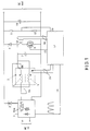
- the incoming a.c. mains voltage 'AC in' passes an input circuit 1, including a rectifier circuit, a high-frequency rejection filter and a making-current limiting circuit. Coupled to the output of the input circuit are a coil 3, a semiconductor switch 8 and a rectifier diode 9, connected as a boost-converter. At the output of the power factor correction circuit, a smoothing capacity 10 is included. To the output terminals 'DC out' the load is connected. The windings 4 and 5 of coil 3 can be connected in series or in parallel via relay contacts 6a and 6b. Included in series with semiconductor switch 8 is a current transformer 13, whose output is connected to a regulating circuit 17.
- a capacity 7 may be connected in parallel to the semiconductor switch element 8.
- a signal 19 originating from coil 3 indicates demagnetization of this coil.
- the output voltage 'DC out' is presented to regulating circuit 17 via voltage divider 11, 12.
- Via signal line 15, the control electrode of semiconductor switch 8 is controlled.
- a clip diode 2 can divert input voltage peaks to the smoothing capacity 10.
- the current through semiconductor switch 8 always increases from zero or a slightly negative value to a maximum value.
- the duration of conduction is practically constant during half a mains period.
- diode 9 takes over the coil current. Capacity 7 limits the dV/dt during switching off, so that switching losses in, and overvoltage across, semiconductor switch 8 are limited. This is important in particular at full power and 115 V input voltage.
- the current through diode 9 decreases to zero.
- the di/dt involved is relatively low, so that the reverse recovery load remains small. Subsequently, the current through diode 9 decreases still further to a small negative value. When the diode is restored, the voltage across coil 3 reverses polarity.
- the stabilized value of the mains voltage is typically 420 V.
- the current through coil 3 has a triangular course. If the conduction period of semiconductor switch 8 is kept constant during half a mains period, the peak value of the current is proportional to the momentaneous input voltage. The average value of the current flowing at the input of the input high-frequency rejection filter in the input circuit 1, is half this peak value. At a self-induction L3 of coil 3, a conduction period t on of semiconductor switch 8 and input voltage U i , the value of the average input current is
- the circuit behaves like a resistor R i with the value
- This apparent resistor also damps resonances in the input filter.
- the input current must be double the value at 230 V.
- the value L3 at 115 V becomes a quarter of the value at 230 V. That is to say, the value of t on must in both cases be the same to be able to produce the maximum power. Further, in this manner, the copper loss is equal in both these cases, as is the degree of core saturation. The same can be realized by applying two equal coils and connecting them in series or in parallel.
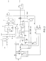
- FIG. 2 A possible embodiment of the control and regulating circuit 17 is shown in Fig. 2.
- An RC oscillator, built up around comparator 26, passes set impulses S to flip-flop 27, whereby via and-gate 28 and via signal line 15 an on-command is given to semiconductor switch 8.
- the conduction is stopped as soon as comparator 33 delivers a reset impulse to flip-flop 27. This last is the case as soon as the sawtooth voltage on capacitor 34 exceeds a limiting value generated by control amplifier 32, or as soon as the current through semiconductor switch 8 exceeds a predetermined limiting value.
- transistor 21 After semiconductor switch 8 has been switched off, through the reversal of the polarity of the voltage across coil 3, transistor 21 is brought into conduction via signal connection 19.
- the circuit round comparator 26 is designed as an RC oscillator, a set impulse /S will even then, after a specific period, be generated, whereupon the semiconductor switch 8 is brought into conduction again. Tnis situation may occur during starting, in the event of overload of the output and in the event of overvoltage on the input. In these circumstances, the current-limiting circuit ensures that the current through the semiconductor switch does not rise to any inadmissibly high values.
- the sawtooth signal on capacitor 34 is obtained through the capacitor 34 being charged via resistor 35 from the relatively high voltage across capacitor 37, obtained from the rectified input voltage. Thus, the incline of the sawtooth voltage is proportional to the peak value of the input voltage.
- transistor 47 comes into conduction and flip-flop 27 is reset via comparator 33, whereupon semiconductor switch 8 is brought out of conduction.
- the current-limiting level at an input voltage of 115 V is approximately twice the current-limiting level at an input voltage of 230 V.
- the output voltage is supplied over signal line 20 and via buffer 29 to MOSFET switch 30. This switch is brought into the conducting position round the zero passages of the mains voltage and then passes the measured value of the output voltage to hold capacitor 31.
- a PI-control amplifier 32 generates the regulating signal whereby the conduction period of semiconductor switch 8 is set.
- Via voltage dividers 38, 39 a signal is added to the reference voltage V ref , ensuring that in the case of small powers, the reset impulses /R become high only on and round the peaks of the mains voltage and remain low beyond them. Accordingly, the boost-converter is only operative on and round the peaks of the mains voltage, so that the maximum operating frequency does not become too high, while yet the requirements described in EN 60555-2 are met.
- circuit 40 determines whether an input voltage of 115 V or 230 V is presented, and operates relay coil 6c and transistors 43 and 44. Also, at switch-on, relay coil 41b is energized. At switch-on and 115 V - 230 V switching, the boost-converter is blocked via signal 42.
- FIG. 3 A possible embodiment of the input circuit is shown in Fig. 3.
- the making-current limiting resistor 46 is bridged by relay contact 41a. Rectification of the input voltage is effected by diodes 49, 50, 51 and 52. Via diodes 53 and 54, signal 14 is generated. Suppression of the disturbing currents generated by the boost-converter is effected by a filter, comprising coils 55 and 57 and capacitors 48, 56 and 58. Clip diode 2 is connected to the junction of the coils 55 and 57. Via a differentiating network, a signal can be derived from signal 14, which is added to the control circuit 32 (Fig.
- the above-described circuit can be omitted. If only a single input voltage is presented or if the difference between minimum and maximum power is relatively small, or if the maximum power is small in the absolute sense, the 115 V - 230 V switch can be omitted. Futher, at minimum load, it will not always be necessary to have the circuit operate only on the peaks of the mains voltage.
- the sample & hold circuit can be omitted in applications where no high control rate is required.
- the sample & hold circuit can also be included after the control amplifier 32.
- the clip diode 2 can also be omitted in certain applications or be replaced by a varistor in the input circuit.
- current limitation can be effected by including a current measuring circuit in the output circuit, such that it measures the current through the coil of the boost-converter, and by connecting the output of this circuit to terminals 18 of Fig. 2. Accordingly, the reset signal will remain active as long as the current through the coil is still above the limiting value, so that semiconductor switch 8 is not brought into the conducting state.
Landscapes
- Engineering & Computer Science (AREA)
- Power Engineering (AREA)
- Rectifiers (AREA)
Applications Claiming Priority (2)
| Application Number | Priority Date | Filing Date | Title |
|---|---|---|---|
| NL9201296A NL9201296A (nl) | 1992-07-20 | 1992-07-20 | Arbeidsfactorcorrectieschakeling. |
| NL9201296 | 1992-07-20 |
Publications (2)
| Publication Number | Publication Date |
|---|---|
| EP0580237A1 true EP0580237A1 (de) | 1994-01-26 |
| EP0580237B1 EP0580237B1 (de) | 1997-10-29 |
Family
ID=19861078
Family Applications (1)
| Application Number | Title | Priority Date | Filing Date |
|---|---|---|---|
| EP93202111A Expired - Lifetime EP0580237B1 (de) | 1992-07-20 | 1993-07-19 | Leistungsfaktorkorrekturschaltung |
Country Status (3)
| Country | Link |
|---|---|
| EP (1) | EP0580237B1 (de) |
| DE (1) | DE69314864T2 (de) |
| NL (1) | NL9201296A (de) |
Cited By (6)
| Publication number | Priority date | Publication date | Assignee | Title |
|---|---|---|---|---|
| EP0732797A1 (de) * | 1995-03-16 | 1996-09-18 | FRANKLIN ELECTRIC Co., Inc. | Leistungsfaktorkorrektur |
| EP1104083A1 (de) * | 1999-11-24 | 2001-05-30 | Lucent Technologies Inc. | Elektrisches Umrichtergerät zur Leistungsfaktorverbesserung |
| EP1229633A1 (de) * | 2001-02-02 | 2002-08-07 | ADI Corporation | Leistungsfaktorkorrekturgerät und Verfahren dafür |
| WO2005002033A1 (en) * | 2003-06-20 | 2005-01-06 | Semiconductor Components Industries, L.L.C. | Power factor control device and method therefor |
| EP2451062A1 (de) | 2010-11-08 | 2012-05-09 | Nxp B.V. | PFC mit Mehrkanal-Fehlerrückmeldung |
| US8644041B2 (en) | 2009-01-14 | 2014-02-04 | Nxp B.V. | PFC with high efficiency at low load |
Citations (1)
| Publication number | Priority date | Publication date | Assignee | Title |
|---|---|---|---|---|
| US4831508A (en) * | 1987-10-20 | 1989-05-16 | Computer Products Inc. | Power supply system having improved input power factor |
-
1992
- 1992-07-20 NL NL9201296A patent/NL9201296A/nl not_active Application Discontinuation
-
1993
- 1993-07-19 DE DE69314864T patent/DE69314864T2/de not_active Expired - Lifetime
- 1993-07-19 EP EP93202111A patent/EP0580237B1/de not_active Expired - Lifetime
Patent Citations (1)
| Publication number | Priority date | Publication date | Assignee | Title |
|---|---|---|---|---|
| US4831508A (en) * | 1987-10-20 | 1989-05-16 | Computer Products Inc. | Power supply system having improved input power factor |
Non-Patent Citations (2)
| Title |
|---|
| GOODENOUGH F.: "PWM CONTROLLER CHIP FIXES POWER FACTOR.", ELECTRONIC DESIGN., PENTON MEDIA, CLEVELAND, OH., US, vol. 37., no. 12., 1 June 1989 (1989-06-01), US, pages 81/82 + 84., XP000039359, ISSN: 0013-4872 * |
| SIEMENS COMPONENTS vol. XXI, no. 3, June 1986, BERLIN DE pages 103 - 107 MICHAEL HERFURTH 'TDA 4814 - Integrated Circuit for Sinusoidal Line Current Consumption' * |
Cited By (8)
| Publication number | Priority date | Publication date | Assignee | Title |
|---|---|---|---|---|
| EP0732797A1 (de) * | 1995-03-16 | 1996-09-18 | FRANKLIN ELECTRIC Co., Inc. | Leistungsfaktorkorrektur |
| US5614812A (en) * | 1995-03-16 | 1997-03-25 | Franklin Electric Co. Inc. | Power supply with power factor correction |
| EP1104083A1 (de) * | 1999-11-24 | 2001-05-30 | Lucent Technologies Inc. | Elektrisches Umrichtergerät zur Leistungsfaktorverbesserung |
| EP1229633A1 (de) * | 2001-02-02 | 2002-08-07 | ADI Corporation | Leistungsfaktorkorrekturgerät und Verfahren dafür |
| WO2005002033A1 (en) * | 2003-06-20 | 2005-01-06 | Semiconductor Components Industries, L.L.C. | Power factor control device and method therefor |
| US8644041B2 (en) | 2009-01-14 | 2014-02-04 | Nxp B.V. | PFC with high efficiency at low load |
| EP2451062A1 (de) | 2010-11-08 | 2012-05-09 | Nxp B.V. | PFC mit Mehrkanal-Fehlerrückmeldung |
| US9712047B2 (en) | 2010-11-08 | 2017-07-18 | Nxp B.V. | Power factor controller with error feedback, and a method of operating such a power factor controller |
Also Published As
| Publication number | Publication date |
|---|---|
| EP0580237B1 (de) | 1997-10-29 |
| NL9201296A (nl) | 1994-02-16 |
| DE69314864D1 (de) | 1997-12-04 |
| DE69314864T2 (de) | 1998-04-30 |
Similar Documents
| Publication | Publication Date | Title |
|---|---|---|
| US5164656A (en) | Switching power supply with constant or sinusoidal input current | |
| JP4613100B2 (ja) | フライフォワード変換器の動作範囲を拡大するための方法及び装置 | |
| US5146399A (en) | Switching power apparatus having high factor and comprising pair of converter for obtaining fixed or variable output voltage | |
| US4652984A (en) | Self-oscillating power-supply circuit | |
| US6295211B1 (en) | Switching power supply unit having delay circuit for reducing switching frequency | |
| CN100399035C (zh) | 测量功率消耗的装置和方法 | |
| US4654771A (en) | Switched power supply comprising a free-running flow converter and electrically separated control loop | |
| US20040051513A1 (en) | Switching regulator with dynamic current limiting and drive circuit for the switching regulator | |
| US4999568A (en) | Switching power supply comprising pair of converters for obtaining constant or sinusoidal input current and fixed or variable output voltage | |
| JPH07163139A (ja) | 高効率スイッチング方式レギュレータ | |
| JPH06225172A (ja) | スイッチモード電源 | |
| US6282103B1 (en) | Switching power supply using an inductor device to prevent harmonic current generation | |
| EP0580237B1 (de) | Leistungsfaktorkorrekturschaltung | |
| JPH01311864A (ja) | スイツチング方式安定化電源回路装置 | |
| US6281669B1 (en) | Circuit arrangement and method for limiting current for consumers of alternating current | |
| JPH06237577A (ja) | コンデンサ充電電源装置 | |
| JP3402031B2 (ja) | 直流電源装置 | |
| JP7175226B2 (ja) | 電源装置 | |
| Kislovski | Fast active inrush current limiter for boost-based resistor emulators | |
| EP1454405B1 (de) | Geregelte frequenzleistungsfaktorkorrekturschaltung und verfahren | |
| JPH0898393A (ja) | 直流電源装置 | |
| JPH0686553A (ja) | 電源回路 | |
| JP2001145338A (ja) | スイッチング電源装置 | |
| US20260012005A1 (en) | Circuit arrangement having an electric device with a magnetizable magnetic core | |
| JP3400160B2 (ja) | スイッチング電源 |
Legal Events
| Date | Code | Title | Description |
|---|---|---|---|
| PUAI | Public reference made under article 153(3) epc to a published international application that has entered the european phase |
Free format text: ORIGINAL CODE: 0009012 |
|
| AK | Designated contracting states |
Kind code of ref document: A1 Designated state(s): DE FR GB NL |
|
| 17P | Request for examination filed |
Effective date: 19940121 |
|
| 17Q | First examination report despatched |
Effective date: 19950908 |
|
| GRAG | Despatch of communication of intention to grant |
Free format text: ORIGINAL CODE: EPIDOS AGRA |
|
| GRAH | Despatch of communication of intention to grant a patent |
Free format text: ORIGINAL CODE: EPIDOS IGRA |
|
| GRAH | Despatch of communication of intention to grant a patent |
Free format text: ORIGINAL CODE: EPIDOS IGRA |
|
| GRAA | (expected) grant |
Free format text: ORIGINAL CODE: 0009210 |
|
| AK | Designated contracting states |
Kind code of ref document: B1 Designated state(s): DE FR GB NL |
|
| ET | Fr: translation filed | ||
| REF | Corresponds to: |
Ref document number: 69314864 Country of ref document: DE Date of ref document: 19971204 |
|
| PLBE | No opposition filed within time limit |
Free format text: ORIGINAL CODE: 0009261 |
|
| 26N | No opposition filed | ||
| REG | Reference to a national code |
Ref country code: GB Ref legal event code: IF02 |
|
| PGFP | Annual fee paid to national office [announced via postgrant information from national office to epo] |
Ref country code: GB Payment date: 20120719 Year of fee payment: 20 |
|
| PGFP | Annual fee paid to national office [announced via postgrant information from national office to epo] |
Ref country code: DE Payment date: 20120720 Year of fee payment: 20 Ref country code: FR Payment date: 20120806 Year of fee payment: 20 |
|
| PGFP | Annual fee paid to national office [announced via postgrant information from national office to epo] |
Ref country code: NL Payment date: 20120716 Year of fee payment: 20 |
|
| REG | Reference to a national code |
Ref country code: DE Ref legal event code: R071 Ref document number: 69314864 Country of ref document: DE |
|
| REG | Reference to a national code |
Ref country code: DE Ref legal event code: R071 Ref document number: 69314864 Country of ref document: DE |
|
| REG | Reference to a national code |
Ref country code: NL Ref legal event code: V4 Effective date: 20130719 |
|
| REG | Reference to a national code |
Ref country code: GB Ref legal event code: PE20 Expiry date: 20130718 |
|
| PG25 | Lapsed in a contracting state [announced via postgrant information from national office to epo] |
Ref country code: DE Free format text: LAPSE BECAUSE OF EXPIRATION OF PROTECTION Effective date: 20130720 |
|
| PG25 | Lapsed in a contracting state [announced via postgrant information from national office to epo] |
Ref country code: GB Free format text: LAPSE BECAUSE OF EXPIRATION OF PROTECTION Effective date: 20130718 |