EP0580347B1 - Tastatur Abfrageeinrichtung - Google Patents
Tastatur Abfrageeinrichtung Download PDFInfo
- Publication number
- EP0580347B1 EP0580347B1 EP93305482A EP93305482A EP0580347B1 EP 0580347 B1 EP0580347 B1 EP 0580347B1 EP 93305482 A EP93305482 A EP 93305482A EP 93305482 A EP93305482 A EP 93305482A EP 0580347 B1 EP0580347 B1 EP 0580347B1
- Authority
- EP
- European Patent Office
- Prior art keywords
- keypad
- interrupt
- microcontroller
- key
- port
- Prior art date
- Legal status (The legal status is an assumption and is not a legal conclusion. Google has not performed a legal analysis and makes no representation as to the accuracy of the status listed.)
- Expired - Lifetime
Links
Images


Classifications
-
- H—ELECTRICITY
- H04—ELECTRIC COMMUNICATION TECHNIQUE
- H04M—TELEPHONIC COMMUNICATION
- H04M1/00—Substation equipment, e.g. for use by subscribers
- H04M1/247—Telephone sets including user guidance or feature selection means facilitating their use
- H04M1/2471—Configurable and interactive telephone terminals with subscriber controlled features modifications, e.g. with ADSI capability [Analog Display Services Interface]
- H04M1/2472—Configurable and interactive telephone terminals with subscriber controlled features modifications, e.g. with ADSI capability [Analog Display Services Interface] with programmable function keys
-
- H—ELECTRICITY
- H03—ELECTRONIC CIRCUITRY
- H03M—CODING; DECODING; CODE CONVERSION IN GENERAL
- H03M11/00—Coding in connection with keyboards or like devices, i.e. coding of the position of operated keys
- H03M11/20—Dynamic coding, i.e. by key scanning
-
- G—PHYSICS
- G06—COMPUTING OR CALCULATING; COUNTING
- G06F—ELECTRIC DIGITAL DATA PROCESSING
- G06F3/00—Input arrangements for transferring data to be processed into a form capable of being handled by the computer; Output arrangements for transferring data from processing unit to output unit, e.g. interface arrangements
- G06F3/05—Digital input using the sampling of an analogue quantity at regular intervals of time, input from a/d converter or output to d/a converter
-
- H—ELECTRICITY
- H03—ELECTRONIC CIRCUITRY
- H03M—CODING; DECODING; CODE CONVERSION IN GENERAL
- H03M11/00—Coding in connection with keyboards or like devices, i.e. coding of the position of operated keys
- H03M11/02—Details
-
- H—ELECTRICITY
- H04—ELECTRIC COMMUNICATION TECHNIQUE
- H04M—TELEPHONIC COMMUNICATION
- H04M1/00—Substation equipment, e.g. for use by subscribers
- H04M1/02—Constructional features of telephone sets
- H04M1/23—Construction or mounting of dials or of equivalent devices; Means for facilitating the use thereof
-
- H—ELECTRICITY
- H04—ELECTRIC COMMUNICATION TECHNIQUE
- H04M—TELEPHONIC COMMUNICATION
- H04M1/00—Substation equipment, e.g. for use by subscribers
- H04M1/72—Mobile telephones; Cordless telephones, i.e. devices for establishing wireless links to base stations without route selection
- H04M1/725—Cordless telephones
- H04M1/73—Battery saving arrangements
-
- H—ELECTRICITY
- H04—ELECTRIC COMMUNICATION TECHNIQUE
- H04W—WIRELESS COMMUNICATION NETWORKS
- H04W52/00—Power management, e.g. Transmission Power Control [TPC] or power classes
- H04W52/02—Power saving arrangements
- H04W52/0209—Power saving arrangements in terminal devices
- H04W52/0251—Power saving arrangements in terminal devices using monitoring of local events, e.g. events related to user activity
- H04W52/0254—Power saving arrangements in terminal devices using monitoring of local events, e.g. events related to user activity detecting a user operation or a tactile contact or a motion of the device
-
- Y—GENERAL TAGGING OF NEW TECHNOLOGICAL DEVELOPMENTS; GENERAL TAGGING OF CROSS-SECTIONAL TECHNOLOGIES SPANNING OVER SEVERAL SECTIONS OF THE IPC; TECHNICAL SUBJECTS COVERED BY FORMER USPC CROSS-REFERENCE ART COLLECTIONS [XRACs] AND DIGESTS
- Y02—TECHNOLOGIES OR APPLICATIONS FOR MITIGATION OR ADAPTATION AGAINST CLIMATE CHANGE
- Y02D—CLIMATE CHANGE MITIGATION TECHNOLOGIES IN INFORMATION AND COMMUNICATION TECHNOLOGIES [ICT], I.E. INFORMATION AND COMMUNICATION TECHNOLOGIES AIMING AT THE REDUCTION OF THEIR OWN ENERGY USE
- Y02D30/00—Reducing energy consumption in communication networks
- Y02D30/70—Reducing energy consumption in communication networks in wireless communication networks
Definitions
- the present invention relates to a keypad scanner mechanism and process and, more particularly, to such a keypad scanner mechanism and process for use in a cordless telephone.
- a keypad is a common device for communicating with a microcontroller or other electronic circuitry and devices.
- the software controlling the microcontroller identifies pressed keys of the keyboard as a signal to the microcontroller to perform certain functions.
- a keypad consisting of an array of keys is essentially a collection of switches, each key forming a switch. Each switch (i.e., key ) may be connected independently to an input port of a device, for example, a microcontroller, to which the keypad serves as an input.
- the interfacing and programming necessary to allow input to the device via the keypad is similar to the interfacing and programming necessary for accomplishing similar results with any other collection of switches.
- the keypad scanner mechanism is the device and process by which the rows and columns of a matrix keypad are examined to determine whether keys have been pressed and, if so, which keys.
- the keypad scanner mechanism detects a number of things that happen. First, the keypad scanner mechanism detects that a key has transmissioned from its open state to its closed state. When pressed, the key will physically bounce (i.e., it will open and close randomly) before it stabilizes in a closed position. The key will be in its depressed state for some period of time, relatively long compared to the time period of the bounce. The keypad scanner mechanism must discern depressions of the key and distinguish from bounce.
- the keypad scanner mechanism detect how long a key is depressed, for example, a volume control which continues to adjust by either increasing or decreasing volume as the key is held down:
- a volume control which continues to adjust by either increasing or decreasing volume as the key is held down:
- the keypad scanner mechanism must detect that the key has been released and report that information to the user. Once so released, the key will bounce again and then go to a stable state of being released, and the keypad scanner mechanism must read such activities.
- keypad reporting systems Prior to the present invention, a variety of keypad reporting systems have been in use. These keypad reporting systems have exhibited certain requirements and characteristics which are restricting or limiting in certain applications, for example, for cordless telephones.
- the requirements and characteristics include high cost of hardware to perform the reporting function and utilization through software of significant amounts of available processing power due to the necessity that functions be performed with a single processor. It would, therefore, be an improvement in the technology if a keypad reporting system were developed which employed more simplified and thus more cost-effective hardware and which allowed for the use of real time software which utilizes a minimum amount of the available processing power thereby allowing use of a smaller, less costly microcontroller that can run at a much lower clock speed thereby limiting power consumption.
- the keypad scanner mechanism of the present invention provides these improvements.
- the standard telephone consists of a base unit panda handset unit connected to each other by an electrical cord.
- the base unit itself is connected by another cord to a receptacle on a wall, telephone pole or a similar immovable structure to which the telephone network line extends. Because of this connection to an immovable structure, the range of movement of the operator of the telephone is quite limited. Even when the cords connecting the handset unit to the base unit and the base unit to the wall are long, it can be cumbersome either to move the entire telephone around to make calls from different locations or to walk around with the handset unit once a call has been placed. The simple fact that there is always a continuous physical connection between the person making the phone call and the immovable wall or other fixed structure can be a great inconvenience.
- the cordless telephone represents a significant improvement over the standard telephone.
- the base unit is still connected to the receptacle on the immovable wall or the like by a cord so that message signals from the telephone network line may be received and transmitted.
- the handset unit of the cordless telephone is an independently operative unit from which calls may be made and by which calls may be received with no physical connection to the base unit.
- the handset unit has a transmitting/receiving system or transceiver, a loudspeaker in an earpiece and a microphone in a mouthpiece.
- the base unit and the handset unit of the cordless telephone communicate with each other over a communication channel established by the transmission and reception of electromagnetic waves, conventionally radio waves.
- the handset unit may then be taken considerable distances from the base unit while still making and receiving telephone calls. Since there is no telephone cord extending between the handset unit and the base unit, the operator is free to move about without hindrance.
- keypad reporting systems have been developed and used, for example, in cordless telephones, to perform various functions. As previously described, however, there are a number of aspects of such keypad reporting systems that can be improved.
- PIA Peripheral Interface Adapter
- the PIA is used to make encoded data form a keyboard available in a PIA Data Register; in the other the PIA is used to read a matrix of keyswitches, a key closure generating an interrupt.
- DE-C1-3641527 discloses a keypad scanner incorporating a microprocessor which is switched into an active mode when one of the keys of the keypad is depressed. Once activity has been detected, the microprocessor identifies and reports the depression of a particular key.
- such a scanner is characterised by software means for debouncing a key depression, the software means
- the mechanism may further comprise a multiple keys down code reported whenever more than one key is simultaneously depressed.
- the mechanism may further comprise a no keys down code reported whenever no key is depressed.
- a method for scanning a pad comprised of more than one key the keypad being incorporated with an integrated circuit including a microcontroller, the method comprising:
- the improved keypad is for use in a base unit and a handset unit of a cordless telephone.
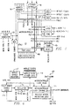
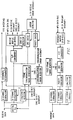
- the keypad scanner mechanism 251 provides the ability to support keypads 300 of up to 36 keys.
- the keypad scanner mechanism 251 includes the following functions:
- the keypad scanner mechanism 251 operates in two modes: 1) activity detect, and 2) normal.
- the activity detect mode the keypad scanner mechanism 251 does not determine which key is depressed, but only when a key has been depressed. This allows the IC (not shown in FIG. 1) to wake up from shut-down mode when the user presses a key.
- An output is generated to the clock generator module 82 (shown in FIG. 2a) when activity is detected while the IC is in shut-down mode.
- the identity of the depressed key is determined and reported, for example, to an input of a microcontroller (not shown) of the IC by means, for example, of a microcontroller bus 258. Debouncing is the responsibility of the user software.
- An interrupt 255 is generated when activity is detected, e.g., when a key is closed.
- the user responds to the interrupt 255 by masking the keypad interrupt, setting a microcontroller timer (debounce time is typically 4 to 16 milliseconds), and returning from the interrupt 255. When the timer expires an interrupt is generated.
- the keypad scanner mechanism 251 module is comprised of the scanner unit 250 and the keypad status register 252.
- the scanner unit 250 contains row and column input pins and comparators, and a block of logic 254 that detects the no keys down, multiple keys down, and any key down conditions. Details of the scanner 250 are as follows: Pins 6 with weak pull-downs (rows) 6 with weak pull-ups (columns) Switch resistance Open ⁇ 150k Ohms Closed ⁇ 2k Ohms No keys down output Active when the outputs of all the row comparators are low. Any key down output Active when the output of any of the row comparators is high. This signal goes to the interrupt controller module.
- the status logic 252 formats the inputs from the scanner unit 250, and presents this status to the user. More specifically, keypad status logic comprises the following:
- the user visible registers include the following keypad status register 259: Address FF2C Size 8 bits Default 00 Hex Access mode Read only Set by Hardware Cleared by Reset This register 259 reports the identity of any single key closure, as well as the no keys down and multiple keys down conditions.
- the keypad status change interrupt 255 request is generated whenever the value of the register 259 changes. The interrupt request is cleared when this register 259 is read.
- BITS 3-1 Column Key Code -- These three bits provide a binary encoding of the key matrix column on which the key is closed. If no keys are depressed, the bits are all zeros. If multiple keys are closed, the bits are undefined. BIT 0 Multiple Keys Down -- This bit is set if more than one key is depressed, otherwise it is cleared.
- the exemplary IC includes an 8-bit microcontroller providing the function of th 80C32T2 member of the 80C51 family of Advanced Micro Devices (AMD) products, which microcontroller will also be discussed herein to the extent as may be relevant to a particular embodiment of the keypad scanner mechanism for use with the exemplary IC.
- AMD Advanced Micro Devices
- the IC has three basic modes of operation. Those three modes are an in-circuit emulation mode, a normal mode, and a test mode.
- the in-circuit emulation capability mode disables the on-chip microcontroller (designated by reference numeral 40 in FIG. 2), allowing an external ICE to be used for software development and software and hardware debugging.
- the normal mode is the mode in which the product containing the IC is operated by the end user.
- a final mode of operation, the test mode is basically the same as the normal mode, except that in the test mode it is possible to also enable internal test functions of the IC.
- Entry into the three operating modes is controlled by the state of the reset pin 42 and the tri-level IN1 (TRI1) pin 44.
- TRI1 pin 44 could effect such selection in a number of different ways, one way would be to have the state of the TRI1 pin be monitored and acted upon by the IC when the reset pin 42 goes inactive. If the TRI1 is low, for example, the in-circuit emulation capability mode could be activated. At a mid supply or no-connect point, the test mode could be activated. Finally, when the TRI1 pin is high and, again, when the reset pin 42 goes inactive, the IC could operate in the normal mode.
- the in-circuit emulation capability mode is triggered at reset if, when the reset pin 42 goes high, the tri-level input 1 pin 44 is low. Further, all interval connections to I/O ports of the exemplary IC are routed from the microcontroller (i.e., "off-chip"), with the exception of the clock connected to the timer 0 and timer 1 inputs (this clock can be external to the IC). ALE and PSEN/ then become inputs. The clock input to the microcontroller, which is routed off chip, is forced on at reset in in-circuit emulation capability mode. The watchdog timer 46 does not operate in this mode.
- the PSEN/pin assumes a high impedance state when the in-circuit emulation capability mode of the IC is triggered.
- Port O it is used in connection with multiplexed address/data bus bits 7-0.
- Port 1 is used for general I/O lines. These lines are mapped to specific control functions by software.
- the Port 1 I/O lines contain a weak pull-up. During emulation mode, the weak pull-ups are disabled and the port pins assume a high impedance state.
- Port 2 is used for address lines 15-18.
- the Port 2 I/O lines contain a weak pull-up. Disabling the weak pull-up is accomplished by setting a corresponding port control register bit (PCRB) to an appropriate value. After RESET, the Port 2 weak pull-ups are enabled. During emulation mode, the weak pull-ups are disabled and the port pins assume a high impedance state.
- PCB port control register bit
- P3.0 is used as either the microcontroller serial port receive data input (RxD) or as a general purpose I/O pin.
- P3.1 is used as either the microcontroller serial port transmit data output (TxD) or as a general purpose I/O pin.
- P3.2 is used internally as an interrupt input from the internal interrupt controller (INTO/).
- P3. 3 is used internally as an interrupt input from the internal interrupt controller (INT1/).
- P3.4 is used as the internal timer 0 clock input. This pin is not available external to the IC.
- P3. 5 is used as the internal timer 1 clock input. This pin is not available external to the IC.
- P3.6 is the WR/ strobe for the address/data bus.
- P3.7 is the RD/ strobe for the address/data bus.
- the Port 3 I/O lines contain a weak pull-up. Disabling the weak pull-up is accomplished by setting a corresponding port control register bit (PCRB) to an appropriate value. After RESET, the Port 3 weak pull-ups are enabled. During emulation mode, the weak pull-ups are disabled and the port pins assume a high impedance state.
- PCB port control register bit
- the Port 1, 2, and 3 I/O buffers are capable of disabling the weakp-channel pull-up through software control.
- the necessity of this function permits the buffers to eliminate current sourcing when the buffer is driven low by an external signal.
- This weak pull-up disabling -feature of the exemplary IC eliminates undesirable power consumption increases.
- the AMD 80C32T2 lacks such a mechanism. After reset, all of the Port 1, 2, and 3 I/O buffers are held "high" by the weak pull-up. This state is functionally compatible with the 80C32T2 microcontroller.
- the software must first disable each bit by configuring the port pin with the corresponding port control register bit.
- the corresponding port control register bit resides at the same address as the port SFR bit.
- Port 1 resides at SFR memory location 90H.
- the Port 1 control register also resides at SFR memory location 90H. Modification of the Port 1 Control Register is only accomplished when the PCRA bit in the PCFIG SFR is set to a "1". When the PCRA bit is cleared, an operation to the Port SFR address results in the Port SFR getting updated.
- Port 0 Since only Ports 1, 2 and 3 contain weak pull-ups, Port 0 its exempt from this feature.
- PCRB PORT BIT FUNCTION 0 0 Drives a "0" output, no pull-up (80C51 compatible) 0 1 Drives a "1" for 2 cycle, weak pull-up is on. (80C51 compatible) 1 0 Drives a "0" output, no pull-up 1 1 Input only, (no pull-up, high impedance input)
- the PCRA bit Upon power-up, the PCRA bit is disabled and any writes to the ports result in the port SFR being updated. Once the PCRA bit in the PCFIG register is set, it becomes possible for each port bit to have the weak p-channel device turned off. After each port bit is appropriately configured, the user must clear the PCRA bit before writing to the ports.
- the port pin may not return to a "1" immediately. This condition is similar to the 80C51 when an external device drives the input signal low and then allows the pin to "float” back to a "1". This rise time of the signal is dependent on the loading of the pin and may take several microseconds to return to a stable "1".
- on-chip RAM in the exemplary IC, such an IC having an 80C32T2 microcontroller has 256 bytes of RAM located in the "Internal Data RAM” space. 1024 bytes of additional "on-chip” RAM is located in “External Data RAM” space. All of the 1024 bytes of on-chip RAM is backed up by the real-time clock's back-up battery. The backed up RAM can support read and write accesses down to 2.2 Volts. The backed up RAM can retain data down to 1.8 Volts.
- interrupt enable during shut-down in the exemplary IC if the IC is in a shut-down mode and the microcontroller is in an idle mode, the condition of the microcontroller's interrupt mask bits (TCON register bits 7, 2, and 0) is ignored, enabling the INTO/ and INT1/ interrupts. The actual TCON bits are not changed to safeguard against the IC entering a shut-down mode with interrupts disabled.
- the ALE I/O pin is multiplexed with the general output bit 9.
- the INTO/OUT and INTI/OUT pins are multiplexed with the external I/O 0 and external RAM chip select outputs, respectively, from the address decoder module 76. During the in-circuit emulation mode, these pins always provide the ALE-OUT, INTO/, and INTI/OUTPUT functions.
- the ALE pin can be either ALE OUT or general output 9. Selection is programmed in the address decoder module. The INTO/ and INT1/ pins are always used as chip select outputs in normal operation.
- a demultiplexed form of the 80C32T2's address bus is constructed by latching the low-order address byte, providing the LATCHED ADDRESS 7-0 pins. The address is latched off of the A/D 7-0 bus on the falling edge of ALE.
- internal timing accounts for the delays associated with bringing A/D 7-0 and ALE on chip when the exemplary IC is in in-circuit emulation mode.
- PO.7-PO.0 is the microcontroller I/O port 0. This port provides the multiplexed D7-0 and A7-0 bus.
- the pins When the exemplary IC is in reset the pins are held weakly high. In shut-down, the pins will either be held strongly low or weakly high. In in-circuit emulation mode the pins are high impedance.
- P1. 7-P1.0 is the microcontroller I/O port 1. This port provides the eight general purpose I/O pins associated with the parallel port module. When the IC is in reset the pins are held weakly high. In shut-down, the pins hold their programmed state. In in-circuit emulation mode the pins are high impedance.
- P2. 7-P2.0 is the microcontroller I/O port 2. This port provides the high order eight bits of the address bus (A15-8). When the IC is in reset or shut-down, the pins are held weakly high. In in-circuit emulation mode the pins are high impedance.
- microcontroller I/O port 3.7 This pin provides the microcontroller RD/ (read, active low) strobe. In in-circuit emulation mode the pin is high impedance. In shut-down or during reset the pin is held weakly high.
- P3.6 is the microcontroller I/O port 3.6. This pin provides the microcontroller WR/ (write, active low) strobe. In in-circuit emulation mode the pin is high impedance. In shut-down or during reset the pin is held weakly high.
- P3.1 is the microcontroller I/O port 3.1. This pin provides the microcontroller's internal serial port transmit data output. The pin can also be used as a general purpose I/O port. In in-circuit emulation mode the pin is high impedance. In reset the pin is held weakly high. In shut-down the pin holds its programmed state.
- P3. 0 is the microcontroller I/O port 3.0.
- This pin provides the microcontroller's internal serial port receive data input.
- the pin can also be used as a general purpose I/O port. In in-circuit emulation mode the pin is high impedance. In reset the pin is held weakly high. In shut-down the pin holds its programmed state.
- PSEN/ is the program store enable. When active, the address on ports 0 and 2 pertains to code space. PSEN/ is placed in a high impedance state in in-circuit emulation mode, and is an output in normal mode. In reset, PSEN/ is held weakly high. In shut-down the pin is held strongly high.
- ALE is the address latch enable. This signal is used to latch the address off of the A/D 7-0 bus. ALE is high impedance during in-circuit emulation mode. ALE is an output, multiplexed with OUT9 during normal mode. In shut-down or reset the pin is held strongly high.
- LATCHED ADDRESS 7-0 is the output of the address latch, providing the non-multiplexed LA7-0 bus. At reset, shut-down, and in in-circuit emulation mode these pins are driven strongly.
- the clock generator 82 (see FIG. 2a) provides the crystal oscillator, power mode control, module enable control, and clock dividers for the exemplary IC.
- the IC is placed into shut-down mode by setting a bit in a shut-down/microcontroller clock control register. After the bit is set the oscillator 72 continues to run for 3.56 - 7.12 milliseconds in order for software to place itself in its idle mode, then all clocks, including the CPUCLK are stopped. In the exemplary IC, the IC terminates the shut-down cycle if an interrupt is received after the enable bit is set, and before the CPU clock is stopped.
- shut-down/microcontroller clock control register access to the shut-down/microcontroller clock control register is protected by an interlock mechanism to reduce the risk of accidental clock stoppage due to software problems.
- This mechanism requires the software to write to a special access control register, and then write the shut-down/microcontroller clock control register. This double-write procedure must be done twice before the clock speed control register is updated.
- Wake-up comes from reset, an any-key-down indication from the keypad scanner 88, the real-time clock interrupt (if not masked within the real-time clock 74), or any non-masked interrupt.
- the oscillator is re-started. A delay of approximately 3.56 milliseconds is required for the oscillator to stabilize. After this delay, the microcontroller 44 and watchdog timer 46 clocks are re-started. The microcontroller clock re-starts at the previously programmed rate.
- the keypad any-key-down and real-time clock interrupts are enabled, even if the associated interrupt enable bits are cleared, i.e., even if the interrupts are disabled.
- the actual interrupt enable bits are not changed.
- the real-time clock interrupts can still be masked within the real-time clock module 74 in the exemplary IC.
- the microcontroller clock in the exemplary IC has a programmable divider with an input of 18.432 MHz.
- the programmable rates are divided by 2, 4, 8, 16, 32, 64, 128, and 256.
- the CPU clock returns to the speed programmed in the control register.
- the CPUCLK can be turned off by placing the IC in shut-down mode.
- the transition to the new frequency is accomplished without producing clock pulses that violate the 80C32T2, or other such appropriate product, data sheet timing specifications.
- the microcontroller clock also has a selectable automatic speed-up mode. -If the automatic speed-up option is selected, all interrupts force the microcontroller clock divider to the divide by two state. After the clock is sped-up, it will remain at the divided by two frequency until the speed is reprogrammed to a lower value. No illegally short pulses are allowed at the frequency transition point.
- the processor clock continues to run for between 3.56 and 7.12 milliseconds before being stopped.
- the clocks to each module are provided by the clock generator module 82. Control bits are provided to allow software to turn on and off specific modules. When a module is turned off, its clock is stopped and held low.
- the serial port 94 supports data rates of 288 kHz, 144 kHz, and 36 kHz.
- the clock provided to the serial port module is divided down to the desired data rate by the clock generator module 82.
- the clock speed is selected via the serial port timing control register.
- the serial port module and this clock are enabled via a module enable control register 0. When the module is disabled, the clock is stopped low.
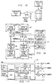
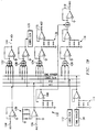
- FIG. 6 is a block diagram of the clock generator module of the exemplary IC.
- the clock generator module directly or indirectly comprises the oscillator 70, shut-down mode control logic 170, microcontroller clock control logic 172, module enables 174, and a module clock divider 176. Each of these is described further in an individual paragraph immediately below.
- the oscillator 70 is designed to run at 18.432 MHz, using a parallel resonant mode crystal. Start-up capacitors are required; however, the exemplary IC minimizes capacitance value to save power.
- the shut-down mode/microcontroller clock control logic 170, 172 controls the entry into shut-down, microcontroller clock frequency, and automatic speed-up.
- register bits to turn on and off specific modules within the IC are located in the clock generator module 82. These bits also stop the clock outputs to their respective modules.
- the module clock divider logic 176 is a divider chain that produces the clock frequencies required by each module.
- the clock generator module 82 has three pins.
- Pin MCLK XTAL is the master clock crystal pin 1. This pin is for input and is on the input side of the oscillator 70.
- the oscillator 70 is designed to work with either a parallel resonant crystal or an external logic level input.
- the MCLK XTAL 2 pin is the master clock crystal pin 2. This pin is for output and is on the output side of the oscillator 70. If a crystal is used, this pin is connected to the crystal. If an external logic level signal is used, this pin is left unconnected.
- the CPUCLKOUT pin is connected to the same clock that feeds the microcontroller 40. It is an output that can be routed off chip. In in-circuit emulation mode, the CPUCLKOUT is always active.
- this clock is multiplexed with the CSOUT2/ signal from the parallel I/O port module.
- the multiplexer control is located in the address decoder module 76 (see FIG. 2b). In reset, this pin defaults to the CSOUT2/ function, and is held high. At shut-down, if the pin is programmed for CPUCLK operation it is held low.
- the clock controller module 82 of the exemplary IC contains the following programmable registers: a shut-down/microcontroller shut-down/microcontroller clock control register; a clock access; a protection register; a module enable control register 1; a module enable control register 2; and a serial port timing control register.
- the addresses of all internal registers as well as the on-chip RAM and the three external chip selects of the exemplary IC are decoded by the address decoder module 76. Enable signals are generated when internal registers or internal RAM is accessed by the microcontroller. Chip selects outputs are generated when external RAM space or either of the two external I/O spaces are accessed.
- the address decoder module 76 of the exemplary IC includes a CSOUT0/pin, a CSOUT1/pin and a CSOUT2/pin.
- the CSOUT0/pin carries a signal which is multiplexed with the INT0/OUT signal. This pin also provides the chip select function when the IC is not in in-circuit emulation mode.
- the CSOUT0/signal is active (low) when a MOVX instruction is executed to the external I/O 1 space. In reset or shut-down this pin is held high.
- the CSOUT1/pin carries a signal which is multiplexed with the INT1/OUT signal. This pin also provides the chip select function when the IC is not in in-circuit emulation mode.
- the CSOUT1/ signal is active (low) when a MOVX instruction is executed to the external RAM space. In reset or shut-down this pin is held high.
- the CSOUT2/pin carries a signal which is multiplexed with the CPUCLKOUT signal. This pin also provides the chip select function when the IC is not in in-circuit emulation mode and the CSOUT2/ enable bit is set in a chip select control register.
- the CSOUT2/ signal is active (low) when a MOVX instruction is executed to the external I/O 2 space. In reset, this pin is held high. If the pin is programmed for CSOUT2/ mode, it is held high in shut-down.
- the aforementioned chip select control register is the only user visible register in the address decoder module 76.
- the decoder module 76 of the exemplary IC includes an address latch and an associated pin.
- the address latch provides the latched form of the low order eight address bits (LADDR 7-0).
- the latched address bus (LADDR 7-0) pins are outputs when the IC is in normal, shut-down, or in-circuit emulation modes. When the IC is in shut-down, the pins are driven strongly with the last value before entering shut-down. The outputs change on the falling edge of ALE.
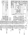
- the interrupt controller 86 of the exemplary IC gathers interrupt requests from various sources internal and external to the IC and generates an interrupt to the microcontroller 40 (INT0/ and INT1/).
- the interrupt system employed in the exemplary IC in which an embodiment of the keypad scanner mechanism capability mode of the present invention may be incorporated has a multilevel structure, including interrupt causes and status registers, a local mask, a local interrupt source register, a main interrupt mask register, and a main interrupt source register. Each of these elements is discussed further in an individual paragraph immediately below.
- interrupt causes and status registers With regard to interrupt causes and status registers, the causes of the interrupts form the lowest level, and are local to each module. These causes can be inputs to pins, conditions such as empty or full data buffers, and the like. The causes are reported in "status registers". A status register, when read by software, always returns the current state of cause signal (for example, the current logic level on an input pin). The bits in a status register are not affected by interrupt masking.
- the cause signals are ANDed with associated mask signals from an "interrupt mask register".
- the output of these AND gates connect to a "local interrupt source register".
- the mask register is located in the module that contains the associated cause signals.
- the local interrupt source register is used by software to determine the cause of an interrupt.
- the bits in the interrupt source register can be set by either rising edge, falling edge, or both edges of the non-masked cause signal.
- the bits in interrupt source registers are cleared separately from each other. In general, each bit is cleared when software responds to the cause. This response can be reading a receive buffer, reading an input port status register, or the like.
- the outputs of each of the register bits is ORed together to produce one interrupt request signal. This signal is sent to the interrupt controller module.
- the source register is located in the module that contains the associated cause signals.
- the interrupt request signals are ANDed with associated mask signals from the "main interrupt mask register" (located in the interrupt controller module 86).
- the output of these AND gates connect to a "main local interrupt source register".
- the main interrupt source register is used by software to determine the cause of an interrupt.
- the bits in the interrupt source register reflect the logic level of the interrupt request signals, provided they are not masked. In general, each interrupt request is cleared when software responds to the specific interrupt cause.
- the outputs of the main interrupt source register are ORed together and forwarded to the microcontroller.
- FIG. 7 shows the structure of the interrupt controller 86 of the exemplary IC.
- Interrupt requests from the logic module 96 see FIG. 2a
- external interrupt inputs such as hookswitch/lock-ups
- the serial I/O 94 the parallel I/O
- keypad scanner 88 and the real-time clock 74 modules feed the two main interrupt source registers 178, 180.
- a master interrupt mask function is provided in the microcontroller in the form of a main mask register 0 182, and a main mask register 1 184.
- Figure 8 shows the structure of the status, mask, and source registers necessary to handle interrupt cause signals from the logic module 96.
- the interrupt controller module 86 of the exemplary IC is comprised of seven user-accessible registers: a main interrupt source register 0 186; a main interrupt mask register 0 188; a main interrupt source register 1 190; a main interrupt mask register 1 192; a D-channel status register 194; a CHM/SYNC mask register 196; and a CHM/SYNC interrupt source register 198.
- the interrupt controller 86 includes an INT0/OUT pin, and an INT1/OUT pin.
- the INT0/OUT signal is an output from the interrupt controller 86 to the microcontroller 40. It is routed off-chip via the INT0/OUT pins. It is used only in in-circuit emulation mode. When the IC is not in in-circuit emulation mode, this pin is used for the chip select zero (CSOUT0) output.
- the INT1/0UT pin carries a signal which is an output from the interrupt controller 86 to the microcontroller 40. It is routed off-chip via the INT1/0UT pin. It is used only in in-circuit emulation mode. When the IC is not in in-circuit emulation mode, this pin is used for the chip select one (CSOUT1) output.
- User accessible registers in the interrupt controller module include the main interrupt source register 0 186; the main interrupt source register 1 190; the main interrupt mask register 0 188; the main interrupt mask register 1 192; the D channel status register; the CHM/Sync interrupt source register 198; and the CHM/Sync mask register 196.
- the watchdog timer 46 detects if the microcontroller software becomes hung-up or lost, and generates a hardware reset to the IC as well as the rest of the system.
- the watchdog timer 46 is not operational in shut-down or in-circuit emulation modes.
- the parallel I/O port of the exemplary IC consists of the microcontroller port 1 interrupt structure, a 11-bit general purpose output latch, 2 tri-level input pins, and three external interrupt inputs.
- the RxD and TxD pins in microcontroller port 3 can also operate as general purpose I/O ports. These ports are organized as discussed immediately below.
- maskable interrupts are programmably generated on one edge of each pin.
- the pins are divided into three separate interrupt source registers, one for P1.7-4, one for P1.3-2, and one for P1.1-0.
- the general purpose outputs are programmed via the general purpose outputs registers 0 and 1.
- the outputs all default high.
- the two tri-level input single pins can report three input states, high, low, or open. Typical applications are dial type selection and factory test mode selection. Additionally, as discussed in considerable detail above, TRI-LEVEL IN1 is used to select in-circuit emulation mode.
- three input pins are provided that generate interrupt requests on both rising and falling edges. These pins can be used for hookswitch, channel synthesizer lock-up, and modem synthesizer lock-up inputs.
- FIG. 11 shows the basic structure of the interrupt function of the exemplary IC.
- the output latch of the exemplary IC provides 11 general purpose output pins for controlling external functions.
- This is a simple pair of registers (one 7-bit and one 4-bit) residing on the microcontroller data bus. When a bit is set in one of the registers (by software), the corresponding output pin is also set. When the bit is cleared, the pin is cleared. All pins that provide one of the general purpose outputs as their default state, default to a high level.
- the multiplexing control for all pins except the keypad (OUT 6,7) and tri-level input (OUT 10) is located in the module where their other function originates, not in the parallel port module (designated by reference numeral 208 in FIG. 11).
- the keypad and tri-level multiplexing is controlled in general purpose output register 1.
- two pins are provided in the exemplary IC that can detect three distinct input states: high, low, and open, or no connect. The state of the input is reported in an external interrupt status register. These pins do not generate interrupt requests.
- the TRI-LEVEL IN1 pin is used primarily for selecting the operating mode of the IC after the RESET pin goes inactive.
- the TRI-LEVEL IN1 pin can be used as a general input in slight variations of the exemplary IC, but extreme care should be taken since a reset could cause the IC to enter the in-circuit emulation mode.
- three interrupt inputs are provided in the exemplary IC that generate interrupt requests on both rising and falling transitions.
- the status of each input pin is reported in a separate one-bit register. If a pin changes state since the last time its status register was read or reset, an interrupt request is latched and sent to the interrupt controller module. Reading the source register clears the latch and thus the interrupt request.
- the 11 outputs of the exemplary IC are independently controlled by their respective bits in the general purpose output control registers 0 and 1. Further, the input pins are pulled to mid-supply (Vcc/2) by pull-up and pull-down resistors when read. The pins each feed a separate pair of comparators. One is biased to produce a high at its output if the input is high, and one is biased to produce a high at its output if the input is low. If the input is open, both comparators output a low state. Still further, it may be noted that the pin logic should be designed to disable the pull-up and pull-down resistors when the state of the pin is not being evaluated. This is a power saving feature.
- the maximum resistance of the external input with respect to Vcc or Vss is 50 Ohms (when the input is high or low). The maximum capacitance is 50 pF.
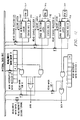
- FIG. 12 there is shown a more detailed view of the external interrupt input structure of the exemplary IC with which the keypad scanner mechanism of the present invention may be included. It may be seen therein that this structure comprises three input pins 220, 222, 224, three status registers 226, 228, 230, and three transition detector latches 232, 234, 236.
- the three external interrupt input status registers 226, 228, 230 which are one-bit registers, report the current status of the external interrupt input pins 220, 222, 224.
- the status bit changes as the pins change. Reading one of the registers clears the associated transition detector latch 232, 234, 236.
- the output of each latch 232, 234, 236 is fed to the interrupt controller module 86 where it is ANDed with an enable bit.
- the serial interface of the exemplary IC is a combination of four serial channels.
- these channels provide communication with frequency synthesizers, an LCD controller, an EEPROM, and a PCM codec test equipment.
- a combined set of transmit, receive, and clock logic is used to support the synthesizer, LCD, EEPROM, and PCM interfaces (see FIG. 12 wherein the transmit, receive and clock logic are generally designated by reference numerals 240, 242 and 246, respectively).
- This combined set of hardware is referred to as the SI/O interface.
- a serial interface is provided for communicating between the on-chip microcontroller and an NEC ⁇ LPD7225 LCD controller IC, or the like. This is also a one direction interface, with communication going only from the IC to the LCD controller.
- the EEPROM interface of the exemplary IC is bidirectional, and is compatible with 8- and 16-bit devices that support the National, General Instruments, Exel interface. Additionally, support for devices that output data on the falling edge of the clock is required. Thus, for compatibility with a wide variety of devices, the port can be programmed to receive data on the rising or falling edge.
- codec test mode the Data In pin becomes the 64 kbps codec receive input
- Data Out pin becomes the 64 kbps codec transmit output
- Clock pin becomes a gated 512 kHz PCM data clock output (bursts of eight cycles at the 8 kHz frame rate).
- the Data In pin becomes the 64 kbps ADPCM transmit input (PCM data input)
- the Data Out pin becomes the 64 kbps ADPCM receive output (PCM data output)
- the Clock pin becomes the 512 kHz PCM data clock output (eight bit bursts at the 8 kHz frame rate).
- the B/D channel port provides the 8 kHz frame sync clock.
- the 64 kHz data clock must be synchronized to the 8 kHz frame sync.
- the PCM test port of the exemplary IC does not use the serial I/O port's transmit buffer, receive buffer, or clock generator.
- the audio path logic provides the clock and a serial transmit bit stream, and receives the receive data in serial form.
- the PCM test function uses the serial I/O port pins, but the logic to support clock generation, clock synchronization, serial to parallel, and parallel conversion is handled within the audio path logic.
- a real-time clock is provided on the exemplary IC.
- This clock 74 (see FIG. 2a) operates from the normal IC supply while the IC is powered on, and from a dedicated battery when the IC is powered down.
- a 32.768 kHz crystal is connected to the real-time clock.
- a 1k byte block of RAM is provided. This "on-chip" RAM is independent from the real-time clock except that it is powered from the real-time clock' s BATT IN pin.
- Figure 14 shows a block diagram of the real-time clock module 74 of the exemplary IC.
- the exemplary IC includes a mechanism providing a digital representation of the power supply (i.e., battery) voltage level over a range of 2.7 to 5.5 volts.
- the power supply i.e., battery
- the battery voltage monitor circuit compares the voltage on a Vcc pin to an internal threshold voltage. If Vcc is above the threshold voltage, the comparator output is high. If Vcc is below the threshold, the comparator output is low.
- the internal threshold voltage is programmable via a 4-bit code from 2.7 Volts to 5.4 Volts, with an accuracy of ⁇ 5%.
- FIG. 17 is a block diagram of the battery level detector module of the exemplary IC.
- the CT2 portion of an exemplary IC which incorporates the in-circuit emulation capability mode of the present invention may include the following modules: FIFOs 90, a B/D Channel Port (see FIG. 2b), a transmit modem 100, an RSSI A/D Converter 92, and a logic module 96.
- two unidirectional FIFOs 260, 262 are provided between the ADPCM block 84, the B channel I/O 264, and the frame formatter 96, with one in the transmit direction and one in the receive direction 262 (see FIG. 16). These fifes provide an elastic store between the 72 kbps radio burst rate and the constant 32 kbps ADPCM, B channel port rate.
- the FIFOs appear to be serial when viewed from the frame formatter 96, and 4 bits wide when viewed by the ADPCM block 84 because the ADPCM operates on nibbles.
- the FIFO module 90 in the exemplary IC builds 512 kHz, 32 kHz, and 8 kHz clocks from either a 1.152 MHz clock from the logic module 96, (specifically, a PLL1152) or a fixed 1.152 MHz clock from the clock generator module 82.
- the B/D Channel I/O Port module 264 in the exemplary IC provides six I/O pins that are multiplexed to serve four separate functions: a B channel I/O port, including encryption; a D channel I/O port; a single transmit (Tx Modulator I/O); and six general purpose output ports.
- the transmit modulator 100 of the exemplary IC accepts serial data from the CT2 logic module 96 and converts it to a quadrature pair of single-ended analog outputs.
- the outputs generated in the exemplary IC are intended to be externally mixed with an IF carrier and summed to obtain the desired frequency modulated signal.
- FIG. 17 A block diagram of the modulator 100 is shown in FIG. 17.
- the heart of the modulator 100 is a look-up ROM 270 addressed by a data dependent state machine address generator 272 and followed by a series of synchronizing latches 274.
- Two identical 6-bit + sign DAC's followed by buffers drive the analog outputs.
- test mode may be provided in the exemplary IC to simplify spectral measurements.
- the receive signal strength indication (RSSI) module 92 provides a digital representation of the RF receive signal level.
- a frame controller which comprises a receive timing recovery, a frame timing generator, a SYNC channel handler, a B channel handler, a D channel handler, and a modem timing adjustment.
- FIG. 18 is a block diagram of the frame controller, including the receive timing recovery, frame timing generator, SYNC channel handler, B channel handler, D channel handler.
- bit synchronized timing from the receive data (Rx Data) is generated and fed to the various functions.
- the SYN channel handler receives a burst signal and the PLLed clock from the receive clock generator (DPLL) and it gives received sync information to the frame timing generator and the CPU. It also receives transmit timing pulses from the frame timing generator, transmit data from the B channel handler and the D channel handler and it generates a transmit burst signal.
- DPLL receive clock generator
- the frame timing generator receives received synchronization information from the syn channel handler when the system is receiving a signal, gives all the necessary receive and transmit timing pulses to the B channel handler, the D channel handler, the SYN channel handler of the transmit portions, MODEM timing adjustment, and any other blocks where those pulses are required.
- the modem timing adjustment measures the delay of the modem and the RF section when they are transmitting and receiving a reference signal from the modem.
- the keypad scanner mechanism of the present invention is well-suited for use in a cordless telephone, when included with an IC to be used in a cordless telephone.
- a cordless telephone of a type into which IC's including the in-circuit emulation capability mode, for example, the exemplary IC previously described, may be incorporated.
- Such a cordless telephone includes a handset or terminal unit 2 (shown in FIG. 19) and a base unit or base station 4 (shown in FIG. 20).
- Base unit 4 is connected by a telephone cord to an outlet or receptacle in a wall, a telephone pole, or another fixed structure, so that it may both receive and transmit telephone message signals through a telephone network line 6 and so that it also may be powered thereby.
- An antenna 8 on the handset 2, and a corresponding antenna 10 on the base station 4 are used to create a communication channel between the two units by the transmission and reception of radio waves.
- handset unit 2 includes a keypad 12 for making or dialing outgoing calls, and a mouthpiece and an earpiece, with which a microphone 14 and a loudspeaker 1 are, respectively, associated.
- a telephone number may be entered on the keypad 12, and corresponding information is transmitted over the communication channel to base unit 4, and thence to the telephone network line 6.
- base unit 4 when base unit 4 receives a message signal from the telephone network line 6 indicating that an incoming call is present, a signal from base unit 4 causes a ringing sound in handset unit 2 and a second ringing sound in base unit 4 to indicate the existence of the incoming call.
- the standard maximum separation of such a handset unit 2 and base unit 4, which is called the service area, is about 300 meters, and is set by the Federal Communications Commission (FCC).
- FCC Federal Communications Commission
- FCC Federal Communications Commission
- the base station 4 like the handset 2, comprises a microphone 22, an ear piece 24, and a keypad 26.
- both the handset 2 and the base station 4 include a ROM 28, 30, an EPROM 32, 34, an LCD and controller 36, 38, as well as a number of other elements which generally relate to the radio signals and power levels.
- an IC including the in-circuit emulator capability mode is used in both the handset unit 2 and the base station 4.
- the IC is designated by reference numeral 18 in FIG. 19 and by reference numeral 20 in FIG. 20.
Landscapes
- Engineering & Computer Science (AREA)
- Theoretical Computer Science (AREA)
- Signal Processing (AREA)
- Human Computer Interaction (AREA)
- Computer Networks & Wireless Communication (AREA)
- Physics & Mathematics (AREA)
- Computer Vision & Pattern Recognition (AREA)
- General Engineering & Computer Science (AREA)
- General Physics & Mathematics (AREA)
- Input From Keyboards Or The Like (AREA)
- Facsimiles In General (AREA)
- Microcomputers (AREA)
- Telephone Set Structure (AREA)
Claims (9)
- Tastaturabfragemechanismus (251) mit einer mehr als eine Taste aufweisenden Tastatur (300), die in einer IC-Schaltung mit einer Mikrosteuereinrichtung (40) enthalten ist, wobei der Mechanismus (251) aufweist:einen Aktivitätsdetektionsmodus, um festzustellen, wann mindestens eine der Tasten betätigt ist, und einen Normal-Modus, der, wenn während des Aktivitätsdetektionsmodus mindestens eine der Tasten betätigt worden ist, dahingehend getriggert wird, daß er die Betätigung der Tasten identifiziert und der Mikrosteuereinrichtung (40) mitteilt, gekennzeichnet durch eine Software-Einrichtung zum Entprellen einer Tastenbetätigung, wobei die Software-Einrichtung(1) ein Interrupt-Signal (255) an einem Interrupt-Port der Mikrosteuereinrichtung (40) empfängt, wenn eine Taste betätigt ist;(2) den Interrupt-Port über ein vorbestimmtes Zeitintervall maskiert; und(3) nach Verstreichen des vorbestimmten Zeitintervalls ein Tastaturstatusregister (259) liest, um die betätigte Taste zu identifizieren.
- Tastaturabfragemechanismus nach Anspruch 1, bei dem die Software-Einrichtung ein Tastatur-Interrupt maskiert, einen Zeitgeber setzt und von dem Interrupt zurückkehrt.
- Tastaturabfragemechanismus nach Anspruch 1 oder 2, bei dem:die IC-Schaltung einen Taktgenerator aufweist; undein Ausgangssignal für den Taktgenerator erzeugt wird, wenn während des Aktivitätsdetektionsmodus Aktivität detektiert wird.
- Tastaturabfragemechanismus nach einem der Ansprüche 1 bis 3, ferner mit einem Mehrfachtastenbetätigungs-Code, der ausgegeben wird, wenn mehr als eine Taste gleichzeitig betätigt ist.
- Tastaturabfragemechanismus nach einem der Ansprüche 1 bis 4, ferner mit einem Nicht-Tastenbetätigungs-Code, der ausgegeben wird, wenn keine Taste betätigt ist.
- Tastaturabfragemechanismus nach einem der Ansprüche 1 bis 5, mit einer Tastaturabfrageeinrichtung mit einem Set von Reihen-Eingängen und einem Set von Spalten-Eingängen, wobei jeder Eingang eines der Sets von Eingängen eine Einrichtung für Schwach-Pull-up aufweist und jeder Eingang des anderen Sets von Eingängen eine Einrichtung für Schwach-Pull-down aufweist.
- Tastaturabfragemechanismus nach einem der Ansprüche 1 bis 6, integriert in eine einzelne IC-Einrichtung für ein schnurloses Telefon.
- Verfahren zum Abfragen einer mehr als eine Taste aufweisenden Tastatur (300), die in einer IC-Schaltung mit einer Mikrosteuereinrichtung (40) enthalten ist, mit den folgenden Schritten:gekennzeichnet durchFeststellen einer Betätigung mindestens einer der Tasten der Tastatur (300); undTriggern eines Wake-up der IC-Schaltung auf die Detektion hin;Entprellen der Tasten mittels einer Software-Einrichtung, dieein Interrupt-Signal an einem Interrupt-Port der Mikrosteuereinrichtung (40) empfängt, wenn eine der Tasten betätigt ist;den Interrupt-Port mittels der Software-Einrichtung über eine vorbestimmte Zeitdauer maskiert; undnach der vorbestimmten Zeitdauer mittels der Software-Einrichtung ein Tastaturstatusregister (259) liest, um die betätigte Taste zu identifizieren.
- Verfahren nach Anspruch 8, bei dem das Maskieren des Interrupt-Ports das Maskieren eines Tastatur-Interrupts, das Setzen einen Zeitgebers und das Zurückkehren von dem Interrupt enthält.
Applications Claiming Priority (2)
| Application Number | Priority Date | Filing Date | Title |
|---|---|---|---|
| US91862592A | 1992-07-21 | 1992-07-21 | |
| US918625 | 1992-07-21 |
Publications (2)
| Publication Number | Publication Date |
|---|---|
| EP0580347A1 EP0580347A1 (de) | 1994-01-26 |
| EP0580347B1 true EP0580347B1 (de) | 1999-02-24 |
Family
ID=25440690
Family Applications (1)
| Application Number | Title | Priority Date | Filing Date |
|---|---|---|---|
| EP93305482A Expired - Lifetime EP0580347B1 (de) | 1992-07-21 | 1993-07-13 | Tastatur Abfrageeinrichtung |
Country Status (6)
| Country | Link |
|---|---|
| US (1) | US5512893A (de) |
| EP (1) | EP0580347B1 (de) |
| JP (1) | JPH0675680A (de) |
| KR (1) | KR100280224B1 (de) |
| CN (1) | CN1062098C (de) |
| DE (1) | DE69323576T2 (de) |
Families Citing this family (19)
| Publication number | Priority date | Publication date | Assignee | Title |
|---|---|---|---|---|
| US5621402A (en) * | 1993-07-21 | 1997-04-15 | Advanced Micro Devices, Inc. | Keypad scanner |
| US5684471A (en) * | 1995-07-24 | 1997-11-04 | Zenith Electronics Corporation | IR remote control transmitter with power saving feature |
| US5900829A (en) * | 1996-07-23 | 1999-05-04 | Motorola, Inc. | Method of and apparatus for detecting key actuations |
| US5798716A (en) * | 1996-08-23 | 1998-08-25 | Motorola, Inc. | Method and apparatus for detecting key actuations |
| US5760714A (en) * | 1996-11-20 | 1998-06-02 | Motorola, Inc. | Interrupt-driven keypad scanning method and apparatus |
| GB2350913B (en) * | 1999-06-10 | 2002-05-29 | John Quentin Phillipps | Combined memory and user input devive |
| US6542092B1 (en) * | 2000-03-06 | 2003-04-01 | Silitek Corporation | Keyboard with multiple input/output function |
| US6744386B2 (en) * | 2000-06-02 | 2004-06-01 | Thomson Licensing, S.A. | Prevention of incompatible keyboard selections from being entered during power initialization |
| US6646576B1 (en) * | 2001-06-26 | 2003-11-11 | Globespanvirata, Inc. | System and method for processing data |
| US20050068303A1 (en) * | 2003-09-30 | 2005-03-31 | Inventec Appliances Corp. | Key inputting circuit of electronic device |
| US20120292367A1 (en) | 2006-01-31 | 2012-11-22 | Ethicon Endo-Surgery, Inc. | Robotically-controlled end effector |
| CN100442893C (zh) * | 2006-03-08 | 2008-12-10 | 华为技术有限公司 | 防止移动终端耳机按键误操作的方法及移动终端 |
| US8992422B2 (en) | 2006-03-23 | 2015-03-31 | Ethicon Endo-Surgery, Inc. | Robotically-controlled endoscopic accessory channel |
| US7809867B2 (en) | 2007-11-14 | 2010-10-05 | Fluke Corporation | Keypad de-bouncing apparatus and method |
| CN101510127B (zh) * | 2009-03-30 | 2012-10-17 | 无锡中星微电子有限公司 | 一种实现键盘模块复合键功能的方法、装置和芯片 |
| CN101989243B (zh) * | 2009-07-31 | 2012-09-05 | 盛群半导体股份有限公司 | 一种集成电路间的数据传输方法 |
| US20140176352A1 (en) * | 2012-12-21 | 2014-06-26 | Apple Inc. | Computer keyboard key scan shared matrix with an individual led per key |
| JP6056576B2 (ja) * | 2013-03-18 | 2017-01-11 | 富士通株式会社 | 割り込み要因を特定する方法及び装置 |
| US9933179B2 (en) | 2014-05-19 | 2018-04-03 | Lennox Industries Inc. | HVAC controller having keypad input and method of operation thereof |
Family Cites Families (10)
| Publication number | Priority date | Publication date | Assignee | Title |
|---|---|---|---|---|
| US4109315A (en) * | 1976-08-30 | 1978-08-22 | Hewlett-Packard Company | Wristwatch calculator with selectively scanned keyboard |
| SE420447B (sv) * | 1978-11-21 | 1981-10-05 | Ibm Svenska Ab | Metod for generering av teckenkoder medelst ett tangentbord samt anordning for utforande av metoden |
| US4301326A (en) * | 1978-11-27 | 1981-11-17 | Hewlett-Packard Company | Controllable cursor vacuum hold down |
| US4731814A (en) * | 1986-02-21 | 1988-03-15 | AT&T Information Systems Inc. American Telephone & Telegraph Company | Computer-controlled cordless telephone |
| CN86103403A (zh) * | 1986-05-14 | 1987-11-25 | 赣州有色冶金研究所 | 一种从稀土矿中提取稀土的新工艺 |
| US4857898A (en) * | 1987-12-09 | 1989-08-15 | North American Philips Consumer Electronics Corp. | Data compression technique for reconfigurable remote control apparatus |
| US4924496A (en) * | 1988-05-12 | 1990-05-08 | Romek Figa D/B/A Abraham & Sons | Automatic incoming telephone call originating number and party display system |
| US5014295A (en) * | 1988-10-28 | 1991-05-07 | Sony Corporation | Multi-channel access cordless telephone system |
| US5192947A (en) * | 1990-02-02 | 1993-03-09 | Simon Neustein | Credit card pager apparatus |
| US5117455A (en) * | 1990-03-28 | 1992-05-26 | Danish International, Inc. | Telephone keypad matrix |
-
1993
- 1993-06-29 JP JP5158417A patent/JPH0675680A/ja active Pending
- 1993-07-13 EP EP93305482A patent/EP0580347B1/de not_active Expired - Lifetime
- 1993-07-13 DE DE69323576T patent/DE69323576T2/de not_active Expired - Lifetime
- 1993-07-20 KR KR1019930013658A patent/KR100280224B1/ko not_active Expired - Fee Related
- 1993-07-21 CN CN93109010A patent/CN1062098C/zh not_active Expired - Fee Related
-
1995
- 1995-06-05 US US08/464,072 patent/US5512893A/en not_active Expired - Lifetime
Also Published As
| Publication number | Publication date |
|---|---|
| CN1083287A (zh) | 1994-03-02 |
| DE69323576D1 (de) | 1999-04-01 |
| EP0580347A1 (de) | 1994-01-26 |
| JPH0675680A (ja) | 1994-03-18 |
| KR100280224B1 (ko) | 2001-03-02 |
| CN1062098C (zh) | 2001-02-14 |
| KR940003243A (ko) | 1994-02-21 |
| DE69323576T2 (de) | 1999-10-21 |
| US5512893A (en) | 1996-04-30 |
Similar Documents
| Publication | Publication Date | Title |
|---|---|---|
| US5555287A (en) | Integrated circuit and cordless telephone using the integrated circuit | |
| EP0580347B1 (de) | Tastatur Abfrageeinrichtung | |
| CA1251517A (en) | Internally register-modelled, serially-bussed radio system | |
| JP2748773B2 (ja) | 電子装置 | |
| AU582196B2 (en) | Method of communications between register-modelled radio devices | |
| CA1287905C (en) | Method and apparatus for detecting a rate of data transmission | |
| EP0582392B1 (de) | Mikrokontroller mit Einrichtung zur Emulation | |
| US5404459A (en) | Serial interface module and method in which the clock is only activated to send a predetermined number of data bits | |
| CN100541465C (zh) | 用于产生多个不同选通脉冲信号的装置及集成电路 | |
| US5950120A (en) | Apparatus and method for shutdown of wireless communications mobile station with multiple clocks | |
| US6125139A (en) | Narrowband digital cordless telephone | |
| US7296186B2 (en) | System-on-chip development apparatus for wire and wireless internet phone | |
| EP0580337A2 (de) | Erhöhungsabschaltmechanismus für Mikrokontroller in integrierten Schaltungen | |
| US5978688A (en) | Apparatus and method for protocol interface | |
| KR100266923B1 (ko) | Tdma 무선 디지탈 통신 시스템에서의 실시간 사상발생 | |
| KR100877735B1 (ko) | 휴대용 통신단말, 휴대용 통신단말의 통신방법과 그프로그램 및 그 프로그램을 기록한 기록매체 | |
| US6298107B1 (en) | Narrowband digital cordless telephone with a logic high weak driver and a logic low strong driver for keypad interface | |
| JP4612205B2 (ja) | 通信システム端末用制御ユニット、この制御ユニットを含むコードレス遠距離通信システムの端末およびその制御方法 | |
| JP5007382B2 (ja) | 無線分離と互換のsimインタフェースを有する通信装置 | |
| JP4701345B2 (ja) | ベースバンド・プロセッサと無線周波数サブシステムにコマンドを送信する方法とベースバンド・プロセッサを内蔵する無線電気通信装置 | |
| KR100231900B1 (ko) | 이동통신 단말기에서 게임기 구현방법 | |
| KR100217738B1 (ko) | 간이 교환장치의 컴퓨터 통신 스피드 향상방법 | |
| KR950000970B1 (ko) | 공통선 신호방식 메세지전달부의 레벨 3기능 구현을 위한 b-버스 입출력보드 | |
| KR20010035849A (ko) | 저소모 전력용 범용 비동기 직렬 데이터 송수신 회로 | |
| Seshan et al. | The advantages of digital signal processors in PCN |
Legal Events
| Date | Code | Title | Description |
|---|---|---|---|
| PUAI | Public reference made under article 153(3) epc to a published international application that has entered the european phase |
Free format text: ORIGINAL CODE: 0009012 |
|
| AK | Designated contracting states |
Kind code of ref document: A1 Designated state(s): BE DE DK ES FR GB GR IE IT LU NL PT |
|
| 17P | Request for examination filed |
Effective date: 19940623 |
|
| 17Q | First examination report despatched |
Effective date: 19960304 |
|
| GRAG | Despatch of communication of intention to grant |
Free format text: ORIGINAL CODE: EPIDOS AGRA |
|
| GRAG | Despatch of communication of intention to grant |
Free format text: ORIGINAL CODE: EPIDOS AGRA |
|
| GRAH | Despatch of communication of intention to grant a patent |
Free format text: ORIGINAL CODE: EPIDOS IGRA |
|
| GRAH | Despatch of communication of intention to grant a patent |
Free format text: ORIGINAL CODE: EPIDOS IGRA |
|
| GRAA | (expected) grant |
Free format text: ORIGINAL CODE: 0009210 |
|
| AK | Designated contracting states |
Kind code of ref document: B1 Designated state(s): BE DE DK ES FR GB GR IE IT LU NL PT |
|
| PG25 | Lapsed in a contracting state [announced via postgrant information from national office to epo] |
Ref country code: NL Free format text: LAPSE BECAUSE OF FAILURE TO SUBMIT A TRANSLATION OF THE DESCRIPTION OR TO PAY THE FEE WITHIN THE PRESCRIBED TIME-LIMIT Effective date: 19990224 Ref country code: GR Free format text: LAPSE BECAUSE OF NON-PAYMENT OF DUE FEES Effective date: 19990224 Ref country code: FR Free format text: LAPSE BECAUSE OF FAILURE TO SUBMIT A TRANSLATION OF THE DESCRIPTION OR TO PAY THE FEE WITHIN THE PRESCRIBED TIME-LIMIT Effective date: 19990224 Ref country code: ES Free format text: THE PATENT HAS BEEN ANNULLED BY A DECISION OF A NATIONAL AUTHORITY Effective date: 19990224 Ref country code: BE Free format text: LAPSE BECAUSE OF FAILURE TO SUBMIT A TRANSLATION OF THE DESCRIPTION OR TO PAY THE FEE WITHIN THE PRESCRIBED TIME-LIMIT Effective date: 19990224 |
|
| REG | Reference to a national code |
Ref country code: IE Ref legal event code: FG4D |
|
| REF | Corresponds to: |
Ref document number: 69323576 Country of ref document: DE Date of ref document: 19990401 |
|
| ITF | It: translation for a ep patent filed | ||
| PG25 | Lapsed in a contracting state [announced via postgrant information from national office to epo] |
Ref country code: PT Free format text: LAPSE BECAUSE OF FAILURE TO SUBMIT A TRANSLATION OF THE DESCRIPTION OR TO PAY THE FEE WITHIN THE PRESCRIBED TIME-LIMIT Effective date: 19990524 Ref country code: DK Free format text: LAPSE BECAUSE OF FAILURE TO SUBMIT A TRANSLATION OF THE DESCRIPTION OR TO PAY THE FEE WITHIN THE PRESCRIBED TIME-LIMIT Effective date: 19990524 |
|
| PG25 | Lapsed in a contracting state [announced via postgrant information from national office to epo] |
Ref country code: LU Free format text: LAPSE BECAUSE OF NON-PAYMENT OF DUE FEES Effective date: 19990713 Ref country code: IE Free format text: LAPSE BECAUSE OF NON-PAYMENT OF DUE FEES Effective date: 19990713 |
|
| EN | Fr: translation not filed | ||
| NLV1 | Nl: lapsed or annulled due to failure to fulfill the requirements of art. 29p and 29m of the patents act | ||
| PLBE | No opposition filed within time limit |
Free format text: ORIGINAL CODE: 0009261 |
|
| STAA | Information on the status of an ep patent application or granted ep patent |
Free format text: STATUS: NO OPPOSITION FILED WITHIN TIME LIMIT |
|
| 26N | No opposition filed | ||
| REG | Reference to a national code |
Ref country code: IE Ref legal event code: MM4A |
|
| PGFP | Annual fee paid to national office [announced via postgrant information from national office to epo] |
Ref country code: GB Payment date: 20010614 Year of fee payment: 9 |
|
| REG | Reference to a national code |
Ref country code: GB Ref legal event code: IF02 |
|
| PG25 | Lapsed in a contracting state [announced via postgrant information from national office to epo] |
Ref country code: GB Free format text: LAPSE BECAUSE OF NON-PAYMENT OF DUE FEES Effective date: 20020713 |
|
| GBPC | Gb: european patent ceased through non-payment of renewal fee |
Effective date: 20020713 |
|
| PG25 | Lapsed in a contracting state [announced via postgrant information from national office to epo] |
Ref country code: IT Free format text: LAPSE BECAUSE OF NON-PAYMENT OF DUE FEES;WARNING: LAPSES OF ITALIAN PATENTS WITH EFFECTIVE DATE BEFORE 2007 MAY HAVE OCCURRED AT ANY TIME BEFORE 2007. THE CORRECT EFFECTIVE DATE MAY BE DIFFERENT FROM THE ONE RECORDED. Effective date: 20050713 |
|
| PGFP | Annual fee paid to national office [announced via postgrant information from national office to epo] |
Ref country code: DE Payment date: 20100728 Year of fee payment: 18 |
|
| PG25 | Lapsed in a contracting state [announced via postgrant information from national office to epo] |
Ref country code: DE Free format text: LAPSE BECAUSE OF NON-PAYMENT OF DUE FEES Effective date: 20120201 |
|
| REG | Reference to a national code |
Ref country code: DE Ref legal event code: R119 Ref document number: 69323576 Country of ref document: DE Effective date: 20120201 |