EP0580481A1 - Verfahren zur Durchführung eines synthesierten Referenzbilds aus in einer CAD-Datenbank gespeicherten Daten - Google Patents
Verfahren zur Durchführung eines synthesierten Referenzbilds aus in einer CAD-Datenbank gespeicherten Daten Download PDFInfo
- Publication number
- EP0580481A1 EP0580481A1 EP93401840A EP93401840A EP0580481A1 EP 0580481 A1 EP0580481 A1 EP 0580481A1 EP 93401840 A EP93401840 A EP 93401840A EP 93401840 A EP93401840 A EP 93401840A EP 0580481 A1 EP0580481 A1 EP 0580481A1
- Authority
- EP
- European Patent Office
- Prior art keywords
- image
- pixels
- binarized
- processing
- construction data
- Prior art date
- Legal status (The legal status is an assumption and is not a legal conclusion. Google has not performed a legal analysis and makes no representation as to the accuracy of the status listed.)
- Withdrawn
Links
Images



Classifications
-
- G—PHYSICS
- G06—COMPUTING OR CALCULATING; COUNTING
- G06T—IMAGE DATA PROCESSING OR GENERATION, IN GENERAL
- G06T7/00—Image analysis
- G06T7/0002—Inspection of images, e.g. flaw detection
- G06T7/0004—Industrial image inspection
- G06T7/001—Industrial image inspection using an image reference approach
-
- G—PHYSICS
- G06—COMPUTING OR CALCULATING; COUNTING
- G06T—IMAGE DATA PROCESSING OR GENERATION, IN GENERAL
- G06T7/00—Image analysis
- G06T7/10—Segmentation; Edge detection
- G06T7/136—Segmentation; Edge detection involving thresholding
-
- G—PHYSICS
- G06—COMPUTING OR CALCULATING; COUNTING
- G06T—IMAGE DATA PROCESSING OR GENERATION, IN GENERAL
- G06T2207/00—Indexing scheme for image analysis or image enhancement
- G06T2207/10—Image acquisition modality
- G06T2207/10056—Microscopic image
-
- G—PHYSICS
- G06—COMPUTING OR CALCULATING; COUNTING
- G06T—IMAGE DATA PROCESSING OR GENERATION, IN GENERAL
- G06T2207/00—Indexing scheme for image analysis or image enhancement
- G06T2207/30—Subject of image; Context of image processing
- G06T2207/30108—Industrial image inspection
- G06T2207/30148—Semiconductor; IC; Wafer
Definitions
- the present invention relates to a method for detecting the defects of an object by comparison, pixel by pixel, between a real image of said object and a reference image synthesized from digital data contained in a CAD database.
- Such a method finds numerous applications in the field of industrial inspection where it is sought to control an object by comparison of the image of said object with the synthesized reference image.
- this invention can be applied to the detection of faults in integrated circuits manufactured from an industrial production line and, in particular, to the detection of defects in reticles used in the semiconductor industry or their imprint. engraved on a silicon wafer.
- Reticle defects may appear during the manufacture of the reticles themselves, or accidentally during handling or periodic or contamination cleaning operations.
- Defects appearing during manufacturing can be detected directly on the reticles by automatic mask and reticle inspection machines of the KLA 219® type.
- Defects appearing after the reticles have been manufactured can be detected by automatic defect inspection machines on silicon wafers of the KLA 2030® type, during a special operation known as "Reticle Qualification".
- This operation consists in inspecting the imprint of the reticle on a layer deposited and etched on a silicon wafer.
- This layer may be either a layer of photosensitive resin after exposure and development, or a layer of silicon oxide or nitride after etching of the layer protected by the resin mask.
- Checking the reticles consists in checking the compliance of the reticle at the end of manufacture with the data used for its description, and in checking that it is free from any defect outside of the tolerance ranges.
- Another known solution consists in controlling the imprint by means of an automatic inspection machine in “chip-to-chip” mode for multi-chip reticles, that is to say for reticles comprising several identical circuits on the same glass plate.
- This chip-by-chip inspection mode consists in comparing pixel by pixel two of the chips located on the glass plate.
- This type of inspection has the advantage of being significantly more efficient than simple visual control by an operator. Indeed, due to the high speed of automatic inspection machines, it is possible to use higher resolution objectives which make it possible to detect faults which are not visible with the aid of low power objectives. In addition, the reliability of the inspection is significantly increased.
- the reference image thus obtained from the data of the CAD database is a synthetic image.
- an image is not always sufficiently precise compared to reality.
- the present invention provides a method for obtaining, from the CAD database, a synthetic image very faithful to the real image of the object acquired by an image acquisition means, such as a optical microscope associated with a CCD camera.
- automatic inspection by comparison of images from the CAD database, consists in producing a synthetic image as faithful as possible to the real image of the object to be inspected and then to compare the two images, pixel by pixel, using the same procedure as chip-by-chip inspection.
- the synthetic image is obtained by seeking to reproduce the degradations induced by the entire physical process which leads digital data contained by the CAD database to an image substantially identical to the real image.
- the sensor of the acquisition system for example, the optical microscope associated with a CCD camera.
- the method according to the invention proposes to reproduce these degradations in order to obtain a synthetic image very close to the real image of the object to be inspected.
- the step of processing the binarized image consists in producing a degraded image in which the patterns of the binarized image are modified according to their relative position in said image, and then to code, from this degraded image, the distances between the pixels of one of the patterns of the degraded image and the pixels of the neighboring patterns to produce the image of levels.
- the degraded image is obtained by application of a convolution operation.
- the degraded image is obtained by application of a mathematical morphology operation.
- the step of processing the binarized image consists in applying a single operation of convolution of said binarized image by means of a finite impulse response filter to produce the image of levels.
- the method of the invention is applied in an automatic device for inspecting faults in an object by comparing an image of the object acquired by the photographing means with the reference image. thus synthesized.
- FIG. 1 represents a functional diagram of the steps of the method for detecting faults of an object, in which the method for producing a synthesized reference image according to the invention is integrated.
- an optical observation microscope 10 is used, coupled to an image acquisition device 20 (also called image-taking means).
- This optical microscope 10 is used, in particular, to inspect the relatively fine patterns of the silicon wafer.
- the image acquisition device 20, such as a CCD camera makes it possible to acquire a real image of areas of the silicon wafer and, more precisely, of the patterns of the silicon wafer which it is sought to inspect. .
- the real image obtained at 20 by the image acquisition device is stored in block 30 as an image to be inspected.
- an image of synthesis obtained in block 50 is used to produce a model image which will serve as a reference image during the comparison with the image to be inspected in order to determine the defects of said image to be inspected.
- This model image is obtained in block 60.
- This synthesis image is produced in block 50 by an image synthesis device coupled to a data storage device, referenced 40.
- This data storage device 40 contains the digital data coming from the CAD database in which the integrated circuit to be inspected is described.
- a digital image INUM is produced by the image synthesis device from digital data contained in the storage device 40. This digital image INUM corresponds to the area of the circuit to be inspected located under the objective of the microscope 10.
- the image to be inspected from block 30 and the model image from block 60 are introduced into block 70 where the detection of the differences existing between said image to be inspected and model image is carried out.
- FIGS. 2A, 2B, 2C and 2D the intermediate images obtained in the different stages between the production of the binary image and the creation of the synthetic image (or synthesized image) used for comparison with the model image.
- FIG. 2A is a representation of the digital image INUM obtained from the data contained in the CAD database.
- This digital image is a binary or pseudo-binary image.
- the production of this digital INUM image is carried out according to a method known to those skilled in the art.
- This digital image contains the geometries contained in the CAD database, that is to say without any degradation of any kind.
- This digital image, in FIG. 2A, is therefore produced by an operation known to those skilled in the art and described in "Advanced 5 x reticle inspection technologies for ULSI devices", TAKEUCHI, JOSEPH, YOSHIDA, MORRIZUMI, PARKER and WATAKABE , published in 1990 in the journal SPIE vol. No. 1261.
- the following operation consists in producing a degraded image of the digital image.
- This image will be called the "morphological image” IMORPH.
- the purpose of this operation is to cause a morphological transformation of the digital image INUM by an operation which reproduces the degradation due to the lithography process used to engrave the geometries on the silicon substrate.
- This operation which is called “morphological transformation operation” reproduces the degradation due to the limited resolution of the lithography processes, as it has already been described previously.
- FIG. 2C represents an image of level INIV, that is to say an image on which are represented the various curves of light levels, also called “isophotic lines". These light level curves reproduce the iso-intensity lines of the image to be inspected, that is to say the lines delimiting areas of the image with identical gray levels.
- the contour lines represent equidistant lines, that is to say lines where the value of the pixels depends only on the distance of this pixel from to the nearest geometry.
- the contour lines are influenced by the local geometry topology.
- the 2D image represents the final ISYN synthesis image, that is to say the synthesis image obtained when the processing of block 50 of FIG. 1 has been entirely carried out.
- This ISYN synthetic image is produced by an operation for generating the final synthetic image which consists in assigning to each pixel of the image of levels INIV of FIG. 2C, a value corresponding to the values of the pixels located on the lines of corresponding light levels of the images acquired in the image acquisition block 20.
- This ISYN final synthesis image is therefore obtained by introducing parameter values read from a real image during a learning operation.
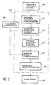
- the block 50 for producing the ISYN synthesis image comprises sub-blocks including, in particular, the sub-block 51 which ensures the generation of the digital image INUM from the database.
- This digital image is a binary, or pseudo-binary, image obtained from CAD data contained in the data storage device.
- the binary or pseudo-binary image thus created is coded according to a grid whose pitch is identical to the pitch of the grid used to describe the reticle of the integrated circuit contained in the CAD database.
- the binary or pseudo-binary image can be created in a grid whose pitch is a multiple of the pitch of the CAD grid; it can even be created directly in a grid, the pitch of which is equal to the pitch of the mesh of the acquisition sensor, that is to say of the mesh of the photographing means.
- the digital image INUM obtained in this block 51 is introduced into the block 53 for generating the morphological image IMORPH.
- this block 53 are also introduced the learning parameters obtained at 25 from the acquisition of the real image of the object to be modeled.
- the morphological image IMORPH is generated from a convolution operation whose mathematical expression is given in the following description.
- the morphological image IMORPH When the morphological image IMORPH has been generated in block 53, it is introduced into block 55 for creating the level image.
- This block 55 makes it possible to assign to each pixel of the IMORPH image a value which depends on the position of this pixel with respect to the surrounding geometries.
- the pixels of the morphological image IMORPH which are distant from any transition, are assigned a value which only depends on the geometry to which said pixel belongs. These pixels can only take two values depending on whether the geometry to which they belong is a background type geometry or a pattern type geometry.
- block 55 allows a value to be assigned to each pixel of the IMORPH image which only depends on the distance between said pixel and the nearest transition.
- block 55 makes it possible to assign to each of said pixels of the morphological image a value which does not depend not only on the distance from the nearest geometry, but also on the local topology of the geometries.
- This block When the INIV level image has been generated in block 55, it is introduced in blocking block 57. This block also receives, as input, the learning parameters obtained at 25 by a learning operation which will be described later.
- This matching block 57 makes it possible to assign the pixels of the image of levels INIV a value according to a correspondence table containing the pixel values of the iso-intensity lines contained by the real image supplied by the image acquisition means.
- the mapping step is performed by means of a mapping table containing predetermined values in the learning operation described later. It is possible to transcode the values of the level image using this correspondence table.
- This correspondence table makes it possible, in a very simple manner, to modify the value of the pixels contained in the image of levels INIV according to a distribution law known and defined by the content of the table.
- the image from block 57 is introduced into resampling block 59.
- This resampling block 59 makes it possible to adapt the coding grid of the ISYN synthesized image obtained at the output of block 57, to the coding grid of the image to be inspected, in order to allow the pixel-to-pixel comparison of said image. synthesis with said image to be inspected.
- the synthetic image is obtained in a grid identical to the grid used to code the data contained in the CAD database.
- This resampling step 59 is useful in order to put the synthetic image ISYN and the image to be inspected in the same "format", that is to say a format where the images are formed of pixels of the same size, which makes them suitable for pixel-to-pixel comparison.
- FIG. 4 represents the flow diagram of a preferred embodiment of the method according to the invention.
- step 55 of creation of the INIV level image is produced simultaneously with the operation for generating the morphological image 53. More precisely, in block 53, a convolution is carried out making it possible both to generate the morphological image IMORPH and to create the INIV level image.
- This operation of convolving the digital image INUM is carried out by a finite impulse response filter.
- each pixel depends only on the distance from this pixel to the nearest geometry.
- the value of each pixel also depends on the local topology of the geometries, that is to say ie the position of the geometries between them.
- this step 54 it is possible to carry out this step 54 using an averaging filter expressed in the form: which has a form similar to the expression of the finite impulse response filter, but where the coefficients C (k, l) are equal to 1.
- This learning operation makes it possible to obtain the characteristics of the convolution kernel used in block 54 and the associated correspondence table TAB.
- the advantage of such a method is that it is easy to implement on an electronic device because the digital processing carried out on the images requires only simple digital operators.
- the digital operators used for this processing are operators known to those skilled in the art and easy to find on the market, which has the effect of allowing a relatively low cost for the device for implementing the method according to the invention.
Landscapes
- Engineering & Computer Science (AREA)
- Computer Vision & Pattern Recognition (AREA)
- Physics & Mathematics (AREA)
- General Physics & Mathematics (AREA)
- Theoretical Computer Science (AREA)
- Quality & Reliability (AREA)
- Image Processing (AREA)
Applications Claiming Priority (2)
| Application Number | Priority Date | Filing Date | Title |
|---|---|---|---|
| FR9208920A FR2693813B1 (fr) | 1992-07-20 | 1992-07-20 | Procédé de réalisation d'une image de référence synthétisée à partir de données contenues dans une base de données CAO. |
| FR9208920 | 1992-07-20 |
Publications (1)
| Publication Number | Publication Date |
|---|---|
| EP0580481A1 true EP0580481A1 (de) | 1994-01-26 |
Family
ID=9432047
Family Applications (1)
| Application Number | Title | Priority Date | Filing Date |
|---|---|---|---|
| EP93401840A Withdrawn EP0580481A1 (de) | 1992-07-20 | 1993-07-16 | Verfahren zur Durchführung eines synthesierten Referenzbilds aus in einer CAD-Datenbank gespeicherten Daten |
Country Status (3)
| Country | Link |
|---|---|
| EP (1) | EP0580481A1 (de) |
| FR (1) | FR2693813B1 (de) |
| IL (1) | IL106267A0 (de) |
Cited By (3)
| Publication number | Priority date | Publication date | Assignee | Title |
|---|---|---|---|---|
| EP0952488A3 (de) * | 1998-04-24 | 2002-07-10 | Nec Corporation | Gerät zum Prüfen von Masken mit reduzierter Prüfzeit |
| WO2019030449A1 (fr) * | 2017-08-10 | 2019-02-14 | Safran | Procédé de contrôle automatique non destructif de pièces mécaniques |
| US12123003B2 (en) | 2018-04-19 | 2024-10-22 | Checkmate Pharmaceuticals, Inc. | Synthetic RIG-I-like receptor agonists |
Citations (2)
| Publication number | Priority date | Publication date | Assignee | Title |
|---|---|---|---|---|
| EP0054598A1 (de) * | 1980-12-18 | 1982-06-30 | International Business Machines Corporation | Verfahren zum Untersuchen und automatischen Sortieren von Objekten bestimmter Gestalt mit festen dimensionalen Toleranzen und Einrichtung zur Durchführung des Verfahrens |
| EP0381067A2 (de) * | 1989-01-31 | 1990-08-08 | Schlumberger Technologies, Inc. | Verfahren zur C.A.D.-Modellspeicherung auf Videobildern mit Addierung der Unordnung |
-
1992
- 1992-07-20 FR FR9208920A patent/FR2693813B1/fr not_active Expired - Fee Related
-
1993
- 1993-07-07 IL IL106267A patent/IL106267A0/xx unknown
- 1993-07-16 EP EP93401840A patent/EP0580481A1/de not_active Withdrawn
Patent Citations (2)
| Publication number | Priority date | Publication date | Assignee | Title |
|---|---|---|---|---|
| EP0054598A1 (de) * | 1980-12-18 | 1982-06-30 | International Business Machines Corporation | Verfahren zum Untersuchen und automatischen Sortieren von Objekten bestimmter Gestalt mit festen dimensionalen Toleranzen und Einrichtung zur Durchführung des Verfahrens |
| EP0381067A2 (de) * | 1989-01-31 | 1990-08-08 | Schlumberger Technologies, Inc. | Verfahren zur C.A.D.-Modellspeicherung auf Videobildern mit Addierung der Unordnung |
Cited By (4)
| Publication number | Priority date | Publication date | Assignee | Title |
|---|---|---|---|---|
| EP0952488A3 (de) * | 1998-04-24 | 2002-07-10 | Nec Corporation | Gerät zum Prüfen von Masken mit reduzierter Prüfzeit |
| WO2019030449A1 (fr) * | 2017-08-10 | 2019-02-14 | Safran | Procédé de contrôle automatique non destructif de pièces mécaniques |
| FR3070084A1 (fr) * | 2017-08-10 | 2019-02-15 | Safran | Procede de controle automatique non destructif de pieces mecaniques |
| US12123003B2 (en) | 2018-04-19 | 2024-10-22 | Checkmate Pharmaceuticals, Inc. | Synthetic RIG-I-like receptor agonists |
Also Published As
| Publication number | Publication date |
|---|---|
| FR2693813B1 (fr) | 1994-08-19 |
| IL106267A0 (en) | 1993-11-15 |
| FR2693813A1 (fr) | 1994-01-21 |
Similar Documents
| Publication | Publication Date | Title |
|---|---|---|
| EP0054598B1 (de) | Verfahren zum Untersuchen und automatischen Sortieren von Objekten bestimmter Gestalt mit festen dimensionalen Toleranzen und Einrichtung zur Durchführung des Verfahrens | |
| FR2715241A1 (fr) | Procédé et dispositif de compensation de déformations dans un système d'inspection optique automatique. | |
| FR2524162A1 (fr) | Appareil et procede de controle de negatifs et dispositif de cadrage de masques | |
| FR2791775A1 (fr) | Detection de defauts a base de particularites | |
| CN114119554A (zh) | 一种基于卷积神经网络的表面微缺陷检测方法及装置 | |
| JP2000329709A (ja) | ワークピース表面の欠陥検査装置及び方法 | |
| WO2002093200A2 (en) | Advanced phase shift inspection method | |
| JP2020024224A (ja) | フォトマスクブランクの欠陥検査方法、選別方法及び製造方法 | |
| WO2007075496A2 (en) | System and method for conducting adaptive fourier filtering | |
| EP3555602B1 (de) | Verfahren zur charakterisierung durch cd-sem-rasterelektronenmikroskopie | |
| WO2006112466A1 (ja) | 鏡面基板の異物検査方法 | |
| JP2004354250A (ja) | 欠陥検査装置 | |
| CN120431401B (zh) | 基于多模态深度学习的晶圆混合型缺陷检测方法和系统 | |
| CN117115095A (zh) | 一种实现复杂纹理瓷砖细小缺陷检测的方法及系统 | |
| JP2023533767A (ja) | デジタルホログラム再構成システム及び方法 | |
| TW202300900A (zh) | 以經呈現設計影像之設計照護區域之分段 | |
| US12361536B2 (en) | EUV mask inspection device, EUV mask inspection method, non-transitory computer-readable medium storing EUV mask inspection program, and EUV mask inspection system including a gray image based on design data of a pattern | |
| KR20230173571A (ko) | 박리 결함에 대한 에지 프로파일 검사 | |
| US7046352B1 (en) | Surface inspection system and method using summed light analysis of an inspection surface | |
| FR2693813A1 (fr) | Procédé de réalisation d'une image de référence synthétisée à partir de données contenues dans une base de données CAO. | |
| US6625800B1 (en) | Method and apparatus for physical image based inspection system | |
| JP2009523241A (ja) | 光学系での人為的分解能(artificialresolution)向上のための装置、方法、及びコンピュータ・プログラム | |
| FR2551210A1 (fr) | Procede de controle d'un reseau | |
| US20250123555A1 (en) | Method and system to for rapid inspection of photolithography reticle | |
| BE1015708A3 (fr) | Procede pour mesurer la hauteur de spheres ou d'hemispheres. |
Legal Events
| Date | Code | Title | Description |
|---|---|---|---|
| PUAI | Public reference made under article 153(3) epc to a published international application that has entered the european phase |
Free format text: ORIGINAL CODE: 0009012 |
|
| AK | Designated contracting states |
Kind code of ref document: A1 Designated state(s): DE GB IT NL |
|
| 17P | Request for examination filed |
Effective date: 19940704 |
|
| STAA | Information on the status of an ep patent application or granted ep patent |
Free format text: STATUS: THE APPLICATION IS DEEMED TO BE WITHDRAWN |
|
| 18D | Application deemed to be withdrawn |
Effective date: 19970201 |