EP0580919A1 - Alimentateur à découpage avec modulation de fréquence - Google Patents
Alimentateur à découpage avec modulation de fréquence Download PDFInfo
- Publication number
- EP0580919A1 EP0580919A1 EP92830418A EP92830418A EP0580919A1 EP 0580919 A1 EP0580919 A1 EP 0580919A1 EP 92830418 A EP92830418 A EP 92830418A EP 92830418 A EP92830418 A EP 92830418A EP 0580919 A1 EP0580919 A1 EP 0580919A1
- Authority
- EP
- European Patent Office
- Prior art keywords
- voltage
- circuit
- switching
- frequency
- power supply
- Prior art date
- Legal status (The legal status is an assumption and is not a legal conclusion. Google has not performed a legal analysis and makes no representation as to the accuracy of the status listed.)
- Granted
Links
Images
Classifications
-
- H—ELECTRICITY
- H02—GENERATION; CONVERSION OR DISTRIBUTION OF ELECTRIC POWER
- H02M—APPARATUS FOR CONVERSION BETWEEN AC AND AC, BETWEEN AC AND DC, OR BETWEEN DC AND DC, AND FOR USE WITH MAINS OR SIMILAR POWER SUPPLY SYSTEMS; CONVERSION OF DC OR AC INPUT POWER INTO SURGE OUTPUT POWER; CONTROL OR REGULATION THEREOF
- H02M1/00—Details of apparatus for conversion
- H02M1/42—Circuits or arrangements for compensating for or adjusting power factor in converters or inverters
- H02M1/4208—Arrangements for improving power factor of AC input
- H02M1/4225—Arrangements for improving power factor of AC input using a non-isolated boost converter
-
- H—ELECTRICITY
- H03—ELECTRONIC CIRCUITRY
- H03K—PULSE TECHNIQUE
- H03K7/00—Modulating pulses with a continuously-variable modulating signal
- H03K7/06—Frequency or rate modulation, i.e. PFM or PRM
-
- Y—GENERAL TAGGING OF NEW TECHNOLOGICAL DEVELOPMENTS; GENERAL TAGGING OF CROSS-SECTIONAL TECHNOLOGIES SPANNING OVER SEVERAL SECTIONS OF THE IPC; TECHNICAL SUBJECTS COVERED BY FORMER USPC CROSS-REFERENCE ART COLLECTIONS [XRACs] AND DIGESTS
- Y02—TECHNOLOGIES OR APPLICATIONS FOR MITIGATION OR ADAPTATION AGAINST CLIMATE CHANGE
- Y02B—CLIMATE CHANGE MITIGATION TECHNOLOGIES RELATED TO BUILDINGS, e.g. HOUSING, HOUSE APPLIANCES OR RELATED END-USER APPLICATIONS
- Y02B70/00—Technologies for an efficient end-user side electric power management and consumption
- Y02B70/10—Technologies improving the efficiency by using switched-mode power supplies [SMPS], i.e. efficient power electronics conversion e.g. power factor correction or reduction of losses in power supplies or efficient standby modes
Definitions
- the present invention relates to a switching power supply circuit for direct connection to an AC power outlet and more in general to a frequency modulator circuit which is particularly suited for modulating the switching frequency of a power supply in function of the instantaneous value of a rectified AC voltage.
- the so-called switching type power supplies are widely used circuits in electronic and electromechanical appliances for providing a low-voltage DC supply of electronic circuits through a rectifier circuit which may be directly connected to the AC power outlet without using a step-down transformer.
- the absence of a transformer and the mode of operation of a switching-type power supply circuit causes the generation of electromagnetic disturbances which propagate through the AC power distribution network.
- the main frequency of these disturbances which is related to the switching frequency of the power supply circuit may have a value which interferes with telecommunication systems using the power distribution lines as signal path and may also cause problems in other electronic apparatuses, connected to the AC power distribution network.
- the oscillator employed for determining a certain oscillation frequency of a switching-type power supply circuit i.e. for driving a power switch of the circuit, comprises a ramp generating circuit, the output ramp signal of which is fed to an input of a comparator.
- a reference voltage is applied to another input of the comparator in order to determine a certain triggering threshold of the comparator, which drives the charge and discharge switches of a capacitance of the ramp generator.
- the oscillation frequency is normally pre-established by selecting a value of capacitance and/or resistance suitable to determine a certain RC characteristic for the charge and discharge processes.
- the ramp generator circuit commonly utilizes a constant current generator, that may be composed of a buffer capable of forcing a certain constant current through a resistance. The constant current so generated is mirrored in a charge/discharge network of the capacitor of the ramp generator circuit.
- the modulation of the oscillation frequency, in function of the instantaneous value of the rectified AC voltage, of an oscillator circuit comprising a voltage ramp generator takes place by employing a divider circuit having two inputs and an output.
- a signal representative of the intantaneous AC voltage e.g. of the AC voltage as recified by a normal bridge rectifier
- a voltage representative of the RMS value of the rectified AC voltage is applied to the other input of the divider circuit .
- This output current (I OUT ) generated by the divider circuit is utilized for modulating the oscillation frequency of the oscillator and has an instantaneous value which is proportional to the instantaneous value of the rectified AC voltage (V ist ), "normalized” as referred to its RMS value (V RMS ). Therefore, the value of the output current I OUT advantageously depends only on the design parameters of the circuit and is independent of the actual RMS value of the AC voltage, which notably may vary from country to country.
- the output node of the frequency modulating circuit i.e.
- variable current (I OUT ) generated by the modulating circuit in function of the instantaneous value of the rectified AC voltage.
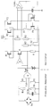
- a typical oscillating circuit commonly used in switching-type power supplies, is composed of a voltage ramp generating circuit and a comparator COMP, the triggering threshold of which may be established by means of a voltage divider formed by R1 and R2.
- the ramp generator circuit comprises a capacitance C, which may be charged by the current delivered by the transistor M3 and discharged through a discharge path, controlled by a switch S1 driven by the comparator COMP, by the current delivered by the transistor M4.
- the frequency of oscillation may be adjusted by establishing a certain charge and discharge current of the capacitance C and this is commonly achieved by utilizing a constant current generator which, as shown, may be composed of a buffer B capable of controlling a transistor MO, which forces a certain current through a resistance R, the value of which may be chosen in function of the desired frequency of oscillation.
- a pre-defined current is mirrored through the transistors M1, M2 and M5 on the charge and discharge transistors M3 and M4 of the capacitance C, respectively.
- a second switch, S2, driven by the comparator COMP has the purpose of connecting R3 in parallel with R2 in order to lower the triggering threshold of the comparator COMP to a certain level of the voltage ramp.
- the frequency of oscillation so pre-defined is modulated in function of the instantaneous value of the rectified AC voltage by employing a frequency modulating circuit (FREQUENCY MODULATOR) composed essentially of a divider circuit, D, having two inputs.
- a first input (V in ) is connected to an intermediate node of a voltage divider formed by the resistances R4 and R5, which is connected across the output nodes of a bridge rectifier, Re, which may be directly connected to the AC outlet.
- a second input is connected to the output node (V RMS ) of a low-pass filter, formed by the network which comprises Ra, Rb and Cf, connected across the output nodes of the bridge rectifier Re.
- the current I OUT produced by the frequency modulator circuit is subtracted to said pre-established charge/discharge current of the capacitance C and therefore, "modulates" the frequency of oscillation between a maximum value (which will correspond to the nominal frequency of oscillation as established by the design of the oscillator circuit) and a minimum value which may be also easily pre-defined and which is reached in coincidence with peak values of the modulating current I OUT produced by the frequency modulator circuit. Therefore, the frequency of oscillation will be variable and notably inversely proportional to the instantaneous value of the rectified AC voltage as normalized in respect to its RMS value.
- the modulating current I OUT produced by the frequency modulator circuit of the invention will have a value which depends exclusively from circuital design parameters and not by the actual RMS value of the AC voltage. Therefore, the switching power supply having a modulated frequency in accordance with the present invention, may be used in different locations also having different AC power distribution standards (e.g. European countries and United States) without any alteration of performance.
- the circuit of the invention may be easily "retrofitted" to an existing oscillator circuit, without the need of redesigning the oscillator circuit.
- the maximum frequency of oscillation may remain the same as determined by an existing oscillator circuit, while the minimum frequency of oscillation, which is achieved by means of the modulating circuit of the invention, will depend exclusively by circuit design parameters and therefore may be easily pre-determined according to need.
Landscapes
- Engineering & Computer Science (AREA)
- Power Engineering (AREA)
- Dc-Dc Converters (AREA)
- Rectifiers (AREA)
Priority Applications (4)
| Application Number | Priority Date | Filing Date | Title |
|---|---|---|---|
| EP92830418A EP0580919B1 (fr) | 1992-07-28 | 1992-07-28 | Alimentateur à découpage avec modulation de fréquence |
| DE69206613T DE69206613T2 (de) | 1992-07-28 | 1992-07-28 | Frequenzmodulierter Schaltnetzteil. |
| US08/098,651 US5555168A (en) | 1992-07-28 | 1993-07-28 | Frequency modulated, switching power supply |
| JP5207185A JPH06233523A (ja) | 1992-07-28 | 1993-07-28 | 周波数変調されたスイッチングパワーサプライ回路 |
Applications Claiming Priority (1)
| Application Number | Priority Date | Filing Date | Title |
|---|---|---|---|
| EP92830418A EP0580919B1 (fr) | 1992-07-28 | 1992-07-28 | Alimentateur à découpage avec modulation de fréquence |
Publications (2)
| Publication Number | Publication Date |
|---|---|
| EP0580919A1 true EP0580919A1 (fr) | 1994-02-02 |
| EP0580919B1 EP0580919B1 (fr) | 1995-12-06 |
Family
ID=8212146
Family Applications (1)
| Application Number | Title | Priority Date | Filing Date |
|---|---|---|---|
| EP92830418A Expired - Lifetime EP0580919B1 (fr) | 1992-07-28 | 1992-07-28 | Alimentateur à découpage avec modulation de fréquence |
Country Status (4)
| Country | Link |
|---|---|
| US (1) | US5555168A (fr) |
| EP (1) | EP0580919B1 (fr) |
| JP (1) | JPH06233523A (fr) |
| DE (1) | DE69206613T2 (fr) |
Cited By (4)
| Publication number | Priority date | Publication date | Assignee | Title |
|---|---|---|---|---|
| EP0670623A3 (fr) * | 1994-03-03 | 1996-06-26 | Miller Electric Mfg | Alimentation commandable. |
| AU679418B1 (en) * | 1996-01-11 | 1997-06-26 | Miller Group, Ltd., The | Series resonant converter, and method and apparatus for control thereof |
| AT408592B (de) * | 1999-08-16 | 2002-01-25 | Felix Dipl Ing Dr Himmelstoss | Verfahren zur nutzung von störsignalen in leistungselektronischen konvertern zur datenübertragung |
| WO2003058797A1 (fr) * | 2002-01-11 | 2003-07-17 | Precisionh2 Inc. | Controleur de facteur de puissance |
Families Citing this family (5)
| Publication number | Priority date | Publication date | Assignee | Title |
|---|---|---|---|---|
| CN1037413C (zh) * | 1993-05-17 | 1998-02-18 | 株式会社久保田 | 滤芯的制造方法 |
| JP2923873B2 (ja) * | 1996-12-03 | 1999-07-26 | 日本電気株式会社 | 圧電トランスの制御方法及び駆動回路 |
| US6636007B2 (en) * | 2001-03-12 | 2003-10-21 | Sunonwealth Electric Machine Industry Co., Ltd. | DC brushless vibration motor |
| US8881685B2 (en) | 2010-03-01 | 2014-11-11 | Robert J. Miavitz | Tug toy |
| TWI508423B (zh) * | 2013-09-06 | 2015-11-11 | Richtek Technology Corp | Power conversion device |
Citations (3)
| Publication number | Priority date | Publication date | Assignee | Title |
|---|---|---|---|---|
| US3946330A (en) * | 1974-04-08 | 1976-03-23 | Victor Company Of Japan, Ltd. | Voltage controlled oscillator circuit |
| WO1985001400A1 (fr) * | 1983-09-19 | 1985-03-28 | Minitronics Pty. Limited | Reduction a un minimum de la teneur en harmoniques pour des inverseurs a semi-conducteurs fonctionnant sur le secteur et attaquant des tubes a decharge gazeuse |
| EP0223315A2 (fr) * | 1985-11-22 | 1987-05-27 | Philips Patentverwaltung GmbH | Disposition de circuit pour produire une tension continue à partir d'une tension d'entrée sinusoidale |
Family Cites Families (3)
| Publication number | Priority date | Publication date | Assignee | Title |
|---|---|---|---|---|
| DE3605025A1 (de) * | 1986-02-18 | 1987-08-20 | Niederberg Chemie | Schlitzwand zur vertikalabdichtung |
| US4816982A (en) * | 1987-11-23 | 1989-03-28 | Viteq Corporation | AC to DC power converter with integrated line current control for improving power factor |
| US5357418A (en) * | 1991-05-02 | 1994-10-18 | Robert Clavel | Hybrid power supply for converting an alternating input signal into a direct output signal |
-
1992
- 1992-07-28 DE DE69206613T patent/DE69206613T2/de not_active Expired - Fee Related
- 1992-07-28 EP EP92830418A patent/EP0580919B1/fr not_active Expired - Lifetime
-
1993
- 1993-07-28 US US08/098,651 patent/US5555168A/en not_active Expired - Lifetime
- 1993-07-28 JP JP5207185A patent/JPH06233523A/ja active Pending
Patent Citations (3)
| Publication number | Priority date | Publication date | Assignee | Title |
|---|---|---|---|---|
| US3946330A (en) * | 1974-04-08 | 1976-03-23 | Victor Company Of Japan, Ltd. | Voltage controlled oscillator circuit |
| WO1985001400A1 (fr) * | 1983-09-19 | 1985-03-28 | Minitronics Pty. Limited | Reduction a un minimum de la teneur en harmoniques pour des inverseurs a semi-conducteurs fonctionnant sur le secteur et attaquant des tubes a decharge gazeuse |
| EP0223315A2 (fr) * | 1985-11-22 | 1987-05-27 | Philips Patentverwaltung GmbH | Disposition de circuit pour produire une tension continue à partir d'une tension d'entrée sinusoidale |
Cited By (7)
| Publication number | Priority date | Publication date | Assignee | Title |
|---|---|---|---|---|
| EP0670623A3 (fr) * | 1994-03-03 | 1996-06-26 | Miller Electric Mfg | Alimentation commandable. |
| US5615095A (en) * | 1994-03-03 | 1997-03-25 | Illinois Tool Works Inc. | Method and apparatus for protecting an inverter power supply |
| US5710696A (en) * | 1994-03-03 | 1998-01-20 | Illinois Tool Works Inc. | Controllable converter power supply |
| AU679418B1 (en) * | 1996-01-11 | 1997-06-26 | Miller Group, Ltd., The | Series resonant converter, and method and apparatus for control thereof |
| AT408592B (de) * | 1999-08-16 | 2002-01-25 | Felix Dipl Ing Dr Himmelstoss | Verfahren zur nutzung von störsignalen in leistungselektronischen konvertern zur datenübertragung |
| WO2003058797A1 (fr) * | 2002-01-11 | 2003-07-17 | Precisionh2 Inc. | Controleur de facteur de puissance |
| US7006367B2 (en) | 2002-01-11 | 2006-02-28 | Precisionh2 Power Inc. | Power factor controller |
Also Published As
| Publication number | Publication date |
|---|---|
| DE69206613T2 (de) | 1996-05-02 |
| EP0580919B1 (fr) | 1995-12-06 |
| DE69206613D1 (de) | 1996-01-18 |
| JPH06233523A (ja) | 1994-08-19 |
| US5555168A (en) | 1996-09-10 |
Similar Documents
| Publication | Publication Date | Title |
|---|---|---|
| EP0201876B1 (fr) | Convertisseur résonant-série | |
| US4980812A (en) | Uninterrupted power supply system having improved power factor correction circuit | |
| US4408268A (en) | Pulse modulated electronic voltage controller with smooth voltage output | |
| US5399955A (en) | Power factor improving arrangement | |
| EP0210310B1 (fr) | Eléments de ballast électronique à contrôle de gain | |
| JPH04331460A (ja) | 電力変換装置 | |
| US4888565A (en) | Apparatus for generating ultrasonic signals | |
| US5459392A (en) | Unity power factor power supply which includes an electromagnetic interference reduction circuit | |
| CA1163677A (fr) | Methode et dispositif de commande pour module d'alimentation resonant | |
| GB2365229A (en) | Blocking control signals outside range in a microwave oven | |
| EP0580919B1 (fr) | Alimentateur à découpage avec modulation de fréquence | |
| US6252784B1 (en) | Power amplifier with feedback | |
| EP0125278B1 (fr) | Alimentation ayant une source de courant continu d'entree et des etages d'alimentation a courant pulse | |
| MXPA04009647A (es) | Regulador de conmutacion de frecuencia de linea. | |
| US4445166A (en) | High voltage converter | |
| DE10124217B4 (de) | Mikrowellenofen | |
| NZ522464A (en) | Control of power drawn by loads supplied by inductive power transfer systems using pick-up means and switch means | |
| GB2320967A (en) | Controlling AC supply voltage | |
| US6101111A (en) | Output power control circuit for a flyback converter | |
| US4523266A (en) | AC to DC conversion system with current spreading circuit | |
| JPH04249892A (ja) | ガス放電ランプを動作させる電力回路 | |
| Bourgeois | Circuits for power factor correction with regards to mains filtering | |
| US6052298A (en) | Inverter input noise suppression circuit | |
| US6703818B2 (en) | AC to AC power converter for electronic devices having substantially different output voltage/current characteristics | |
| US5003456A (en) | Circuit for providing fast output current control in a current mode switching power supply |
Legal Events
| Date | Code | Title | Description |
|---|---|---|---|
| PUAI | Public reference made under article 153(3) epc to a published international application that has entered the european phase |
Free format text: ORIGINAL CODE: 0009012 |
|
| AK | Designated contracting states |
Kind code of ref document: A1 Designated state(s): DE FR GB IT |
|
| 17P | Request for examination filed |
Effective date: 19940727 |
|
| 17Q | First examination report despatched |
Effective date: 19941122 |
|
| GRAA | (expected) grant |
Free format text: ORIGINAL CODE: 0009210 |
|
| AK | Designated contracting states |
Kind code of ref document: B1 Designated state(s): DE FR GB IT |
|
| REF | Corresponds to: |
Ref document number: 69206613 Country of ref document: DE Date of ref document: 19960118 |
|
| ITF | It: translation for a ep patent filed | ||
| ET | Fr: translation filed | ||
| PLBE | No opposition filed within time limit |
Free format text: ORIGINAL CODE: 0009261 |
|
| 26N | No opposition filed | ||
| REG | Reference to a national code |
Ref country code: GB Ref legal event code: IF02 |
|
| PGFP | Annual fee paid to national office [announced via postgrant information from national office to epo] |
Ref country code: DE Payment date: 20020731 Year of fee payment: 11 |
|
| PG25 | Lapsed in a contracting state [announced via postgrant information from national office to epo] |
Ref country code: DE Free format text: LAPSE BECAUSE OF NON-PAYMENT OF DUE FEES Effective date: 20040203 |
|
| PGFP | Annual fee paid to national office [announced via postgrant information from national office to epo] |
Ref country code: FR Payment date: 20040708 Year of fee payment: 13 |
|
| PGFP | Annual fee paid to national office [announced via postgrant information from national office to epo] |
Ref country code: GB Payment date: 20040728 Year of fee payment: 13 |
|
| PG25 | Lapsed in a contracting state [announced via postgrant information from national office to epo] |
Ref country code: IT Free format text: LAPSE BECAUSE OF NON-PAYMENT OF DUE FEES;WARNING: LAPSES OF ITALIAN PATENTS WITH EFFECTIVE DATE BEFORE 2007 MAY HAVE OCCURRED AT ANY TIME BEFORE 2007. THE CORRECT EFFECTIVE DATE MAY BE DIFFERENT FROM THE ONE RECORDED. Effective date: 20050728 Ref country code: GB Free format text: LAPSE BECAUSE OF NON-PAYMENT OF DUE FEES Effective date: 20050728 |
|
| GBPC | Gb: european patent ceased through non-payment of renewal fee |
Effective date: 20050728 |
|
| PG25 | Lapsed in a contracting state [announced via postgrant information from national office to epo] |
Ref country code: FR Free format text: LAPSE BECAUSE OF NON-PAYMENT OF DUE FEES Effective date: 20060331 |
|
| REG | Reference to a national code |
Ref country code: FR Ref legal event code: ST Effective date: 20060331 |