EP0581478A1 - Serieller Schittstellenbaustein und Verfahren zur Datenübertragung - Google Patents
Serieller Schittstellenbaustein und Verfahren zur Datenübertragung Download PDFInfo
- Publication number
- EP0581478A1 EP0581478A1 EP93305454A EP93305454A EP0581478A1 EP 0581478 A1 EP0581478 A1 EP 0581478A1 EP 93305454 A EP93305454 A EP 93305454A EP 93305454 A EP93305454 A EP 93305454A EP 0581478 A1 EP0581478 A1 EP 0581478A1
- Authority
- EP
- European Patent Office
- Prior art keywords
- clock
- data
- serial input
- output port
- data bits
- Prior art date
- Legal status (The legal status is an assumption and is not a legal conclusion. Google has not performed a legal analysis and makes no representation as to the accuracy of the status listed.)
- Granted
Links
Images



Classifications
-
- G—PHYSICS
- G06—COMPUTING OR CALCULATING; COUNTING
- G06F—ELECTRIC DIGITAL DATA PROCESSING
- G06F13/00—Interconnection of, or transfer of information or other signals between, memories, input/output devices or central processing units
- G06F13/38—Information transfer, e.g. on bus
-
- G—PHYSICS
- G06—COMPUTING OR CALCULATING; COUNTING
- G06F—ELECTRIC DIGITAL DATA PROCESSING
- G06F13/00—Interconnection of, or transfer of information or other signals between, memories, input/output devices or central processing units
- G06F13/38—Information transfer, e.g. on bus
- G06F13/42—Bus transfer protocol, e.g. handshake; Synchronisation
- G06F13/4204—Bus transfer protocol, e.g. handshake; Synchronisation on a parallel bus
- G06F13/4221—Bus transfer protocol, e.g. handshake; Synchronisation on a parallel bus being an input/output bus, e.g. ISA bus, EISA bus, PCI bus, SCSI bus
- G06F13/423—Bus transfer protocol, e.g. handshake; Synchronisation on a parallel bus being an input/output bus, e.g. ISA bus, EISA bus, PCI bus, SCSI bus with synchronous protocol
-
- G—PHYSICS
- G06—COMPUTING OR CALCULATING; COUNTING
- G06F—ELECTRIC DIGITAL DATA PROCESSING
- G06F1/00—Details not covered by groups G06F3/00 - G06F13/00 and G06F21/00
- G06F1/04—Generating or distributing clock signals or signals derived directly therefrom
Definitions
- the present invention relates to systems for communicating between microcontrollers and other devices and, more particularly, to systems implementing a serial interface for communicating between an on-chip microcontroller and external devices.
- Serial interfaces involve time-sequential processing of the individual parts as a whole, such as the bits of a character, the characters of a word, and so on, using the same facilities for successive parts.
- Parallel interfaces involve the simultaneous processing of the individual parts of a whole, using separate facilities for the various parts.
- the present invention relates to serial interfaces such as those that can allow an on-chip microcontroller to talk to a number of industry standard external devices, such as serial electrically erasable/programmable read-only memories (EEPROM's).
- EEPROM's electrically erasable/programmable read-only memories
- Such interfaces have been formed relying heavily upon software to control the ports of the microcontroller.
- serial communication system including a serial communication port structure for starting and stopping an internal clock.
- This internal clock is designed, in operation, to generate a clock output signal to be transmitted to a device external to the system in which the serial communication port is incorporated.
- the serial communication port can effectively control the passage of time as sensed by the external device.
- serial input/output port for a microcontroller, which serial input/output port is operable to send data and clock signals to an external device.
- the serial input/output port includes means for determining a select number of data bits to send to the external device, means for producing only enough clock pulses to send the determined select number of data bits, means for beginning production of clock pulses to send the determined select number of data bits, and means for stopping production of clock pulses immediately upon production of only enough clock pulses to send the determined select number of data bits.
- serial input/output port module for a microcontroller, which serial input/output port modules is operable to send data and clock signals to an external device.
- This serial input/output port module includes an internal clock, means for starting the internal clock, means for transmitting a predetermined number of data bits to the external device while the clock is running, and means for stopping the internal clock immediately upon completion of transmission of the predetermined number of bits.
- the method includes the steps of sending a predetermined amount of the data simultaneously with a clock signal to the external device, and stopping the clock signal immediately upon transmission of the last of the predetermined amount of data.
- serial interface is a combination of four serial channels designed to provide communication with frequency synthesizers (such as the Fujitsu MB1501 Frequency Synthesizer), an LCD controller (such as the NEC microPD7225 LCD Controller), an EEPROM (such as a S-2914AR/1 EEPROM), and PCM codec test equipment.
- frequency synthesizers such as the Fujitsu MB1501 Frequency Synthesizer
- LCD controller such as the NEC microPD7225 LCD Controller
- EEPROM such as a S-2914AR/1 EEPROM
- PCM codec test equipment PCM codec test equipment.
- a common set of transmit, receive, and clock logic is used to support the synthesizer, LCD, EEPROM, and PCM interfaces.
- this combined set of hardware is referred to as the serial I/O or SI/O interface.
- the synthesizer interface it should be understood that communication between the IC and the synthesizer chip is unidirectional, from the IC to the synthesizer.
- the Tx Data signal is for serial data output. In actual operation, data is transmitted MSB first, on the falling edge of the clock.
- Shift Clock signal a 50% duty cycle clock can be used. This allows programmable speed, e.g., 288 kbps, 144 kbps, 72 kbps, and 36 kbps.
- the clock is gated on only when data is being sent, and is held high the rest of the time that the module is enabled.
- the Synthesizer Latch signal a "latch" pulse is sent on a dedicated pin after the last bit has been sent. In the actually constructed embodiment of the present invention, this function is supported with a general purpose parallel port pin.
- a serial interface is provided for communicating between an on-chip microcontroller and an LCD controller IC. Like the synthesizer interface, this interface is unidirectional, from the IC to the LCD controller. Five interface signals are supported over this interface.
- a Tx Data signal is used to transmit serial data output in 8-bit words, MSB first.
- the four other signals are a Shift clock, a Chip Select, a Command/Data, and a Busy signal.
- Shift Clock signal in the actually constructed embodiment of the present invention, data is transmitted synchronous to the falling edge of a 50% duly cycle clock (received into the LCD controller on the rising edge, with a one microsecond setup and hold time).
- Clock speed is programmable with 288 kbps, 144 kbps, 72 kbps, and 36 kbps being selectable.
- the clock is gated on only when data is being sent, with eight cycles being output for each byte of data sent. The clock is held high when data is not being sent.
- the Chip Select pin is a software controlled port pin. An active low output on this pin indicates that the data on the Tx Data output pin is intended for the LCD controller.
- the Command/Data and Busy pins are also software controlled.
- the Command/Data pin provides an address line to the LCD controller.
- the Busy pin is used in conjunction with the LCD controller generating a busy strobe to indicate that the LCD controller is free to receive the next data byte.
- the EEPROM interface in the actually constructed embodiment of the present invention is bidirectional, and is compatible with 8- and 16-bit devices that support the National, General Instruments, and Exel interface. Additionally, support for devices that output data on the falling edge of the clock is provided. Thus, for compatibility with a wide variety of devices, the port can be programmed to receive data on the rising or falling edge.
- Four interface pins, a Tx Data, an Rx Data, a Shift Clock, and a Chip Select, are supported.
- the Tx Data pin is for serial data output.
- data is transmitted MSB first, on the falling edge of the clock.
- the word length is from 5 to 28 bits long. Words longer than eight bits can be transmitted in two or more increments.
- an eleven bit word can be transmitted as one byte followed by 3 bits, a 7-bit and a 4-bit word, or even 11 1-bit words.
- the Rx Data pin is for serial data input, which in the system described herein means 8- or 16-bit words, MSB first.
- MSB 16-bit words
- the Shift Clock pin in the actually constructed embodiment of the present invention data is transmitted synchronous to the falling edge of a 50% duty cycle clock.
- the clock output is held high between transmission of parts of the same word.
- Data is received from the EEPROM on either the rising or falling edge of this same clock.
- Clock speed is programmable, with 288 kbps, 144 kbps, 72 kbps, and 36 kbps being possible selections.
- the clock is active only when data is being transmitted. It is held high when stopped.
- the clock continues to run after the transmit part of the sequence until either 8 or 16 bits are received as specified in the SI/O mode register, discussed further below.
- the Chip Select pin is a software controlled port pin, whereupon an active low output indicates that the EEPROM is being accessed.
- the PCM test port interface in the actually constructed embodiment of the present invention, two special modes can be invoked from software that convert the serial port to a codec or an ADPCM transcoder test port.
- a codec test mode the Data In pin becomes the 64 kbps transmit output
- the Clock pin becomes a gated 512 kHz PCM data clock output, i.e., bursts of eight cycles at an 8 kHz frame rate.
- the Data In pin becomes the 64 kbps ADPCM transmit input (or PCM data input)
- the Data Out pin becomes the 64 kbps ADPCM receive output (or PCM data output)
- the Clock pin becomes the 512 kHz PCM data clock output, i.e., eight bit bursts at the 8 kHz frame rate.
- the B/D channel port provides the 8 kHz frame sync clock.
- the 64 kHz data clock must be synchronized to the 8 kHz frame sync.
- the PCM test port does not use the serial I/O port's transmit buffer, receive buffer, or clock generator.
- the audio path logic provides the clock and a serial transmit bit stream, and receives the receive data in serial form.
- the PCM test function uses the serial I/O port pins, but the logic to support clock operation, clock synchronization, serial to parallel, and parallel conversion is handled within the audio path logic.
- transmission may be verified of each of the target SI/O external devices including correct number of clocks for 1 to 8 bits sent, clock stops in correct state, proper set-up time is met when transmission and clocks restart, and proper handling of dummy bit for both rising and falling edge reception.
- Second it may be verified that clocks are turned off in the proper state when the interface is disabled.
- buffer status reporting for SI/O receive and transmit buffers may be verified, and it may be verified that SI/O data is not received at the wrong time.
- PCM mode operation including pin multiplexing, may also be verified.
- Interrupt status reporting including asynchronous read of double buffered receive buffers, may also be verified.
- all register defaults may be verified.
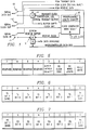
- the embodiment of the present invention shown therein may be seen to comprise a transmit buffer 2, a receive buffer 4, a clock generator 6, a programmable length counter 8, and a mode register (also designated by reference numeral 6). Each of these elements is discussed immediately below.
- an 8-bit long transmit shift register forms part of embodiments of the present invention.
- this register 2 is loaded by software with from 1 to 8 bits of data. The number of bits actually loaded corresponds to the number of bits programmed in the SI/O transmit length register. Data is transmitted MSB first with data bus bit 7 loading the MSB of the shift register. When less than 8 bits are loaded, software locates the bits to be transmitted in the least significant bit positions of the shift register. Transmission begins when the buffer is written if a reception is not in progress, otherwise transmission starts automatically after the read operation is completed.
- software only loads data into the buffer when transmission is not in progress. No error indication is generated if the microcontroller attempts to write to the buffer during transmission. Data is shifted out of the buffer on the falling edge of the shift clock. The output pin is held high when the SI/O interface is enabled and data is not being transmitted. Software transmits a "dummy" low bit if a high start bit is required by the receiving device.
- a status bit is set in the SI/O status register whenever the transmit shift register is empty.
- the status bit is cleared when there is data in the shift register.
- a maskable interrupt is generated whenever this bit is set.
- the software will only enable the interrupt when data has been loaded into the shift register 2 and when there is more than one word to be transmitted. This causes an interrupt to be generated as soon as the last bit has left the shift register, at the end of the last bit time, indicating that a new word can be loaded.
- the number of bits to be transmitted which is from 1 - 8 bits, is specified in the SI/O transmit length register.
- the receive buffer 4 is a single-byte double-buffered register, where data is shifted serially into one half of the buffer pair, and is then automatically transferred into the second half if it is empty. This allows for a double buffer in the case of 8-bit wide EEPROMs, and single buffering when 16-bit wide EEPROMs are used. Data is read from the second half of the buffer pair by the microcontroller.
- Data can programmably be received on the rising or falling edge of the clock. If data is received on the rising edge of the clock, the first bit is received on the second rising edge after the falling edge that outputs the last transmit bit, i.e., 1.5 cycles. If data is received on the falling edge, data is received on the second falling edge after the edge that output the last transmit bit, i.e., two cycles.
- a status bit is set in the SI/O status register whenever there is at least one byte of data in the buffer. The bit is cleared when the register is empty. A maskable interrupt is generated whenever the bit is set.
- the clock generator 6 produces the correct clock output for each of the modes of operation.
- the master input clock to the SI/O clock generator 6 comes from the clock generator module (see FIG. 2a).
- the data rate is programmed in the serial port timing control register located in the clock generator module. Possible data rates include 288 kHz, 144 kHz, 72 kHz, and 36 kHz.
- the input clock is present only when the serial port is enabled, and is held low when the serial port module is disabled.
- the SI/O clock out pin is held low when the serial port is disabled or when the IC is in reset. When active, the output wave form and number of cycles is dependent on the mode of the serial port, as discussed immediately below.
- the clock output is the output of the clock divider ANDed with a control signal from the transmit length counter such that only the desired number of clock pulses are produced for each word to be transmitted.
- the clock output is tied between transmission of parts of the same word. Transmission starts when the transmit buffer is written if a reception is not in progress, otherwise transmission starts automatically after the read operation is completed.
- the clock output is the same as in the transmit mode except that if the read/write bit in the SI/O mode register is sampled as "read" at the completion of the transmit operation, the clock output is left running until the programmed number of bits has been shifted in.
- transmission takes place in sections of from 1 to 8 bits at a time.
- the number of bits in a section is programmed into the SI/O transmit length register prior to loading the transmit buffer.
- the length register does not need to be reprogrammed if successive sections have the same length.
- received words can be 8 or 16 bits in length.
- the desired length is programmed by software into the SI/O mode register.
- the serial port has a SI/O data out pin 10, a SI/O data in pin 12, and a SI/O clock out pin 14.
- the SI/O data out pin 10 is for the data output of the SI/O.
- data is transmitted MSB first, on the falling edge of the clock.
- the SI/O data in pin 12 is for data input for the SI/O.
- data is programmably clocked in on either the rising or falling edge of the SI/O clock.
- the SI/O clock out pin 14 is for clock output for the SI/O. In the actually embodiment of the present invention, this is a gated clock that produces the correct number of transitions for the programmed operation. Thus, it is not free running.
- the pin is held low.
- the serial port module contains some seven user visible registers. These registers include the serial port mode register 6, the SI/O transmit buffer 2, the SI/O receive buffer 4, the SI/O transmit length register 8, as well as an SI/O status register, an SI/O interrupt mask register, and an SI/O interrupt source register.
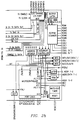
- FIG. 2 there is shown a block diagram of an integrated circuit (IC) including a serial port according to the teachings of the present invention. Because the IC shown in FIG. 2 is discussed at length in a case related hereto, and which has been incorporated by reference herein, the various elements shown in FIG. 2 will not be discussed in detail. However, it is useful for those skilled in the art to note how a serial port (shown as element 16 in FIG. 2) may be connected into an integrated circuit.
- a serial port shown as element 16 in FIG. 2
- the serial port module 16 may be so incorporated into an IC that its SI/O clock out, SI/O data out, SI/O data in, and out 1 serve as an external interface to the IC. It may also be seen that the serial port module receives input from the IC in the form of an out 0 and an out 1 signal. Further, the serial port module according to the teachings of the present invention also receives a 512 k burst clock input signal. This is shown to come from the RX FIFO portion of the IC shown in FIG. 2.
- serial port module according to the teachings of the present invention and shown in FIG. 2 also may be seen to deliver an output to the IC in the form of the serial port interrupt.
- a two-way test signal may be seen to interconnect a codec portion of the IC shown in FIG. 2 and the serial port according to the teachings of the present invention, also shown in FIG. 2.
- FIGs. 3 and 4 shown therein is a terminal or handset portion of a cordless telephone and a base station portion of a cordless telephone, respectively.
- the IC shown in FIG. 2 plays a prominent role in both the terminal and base station portions of the cordless telephone depicted. It may also be seen in FIGs. 3 and 4 how the various input and output signals to the serial port module according to the teachings of the present invention interface with external elements to the IC within the cordless telephone.
- serial port mode register SI/O transmit buffer
- SI/O receive buffer SI/O transmit length register
- SI/O status register SI/O status register
- serial port interrupt mask register serial port interrupt source register
- the present invention provides a serial communication system including a serial communication port structure for starting and stopping an internal clock.
- the internal clock is designed, in operation, to generate a clock output signal to be transmitted to a device external to the system in which the serial communication port is incorporated.
- the serial communication port can effectively control the passage of time as sensed by the external device. Therefore, the present invention provides a simple, low-cost, and flexible serial interface, made primarily of hardware.
Landscapes
- Engineering & Computer Science (AREA)
- Theoretical Computer Science (AREA)
- Physics & Mathematics (AREA)
- General Engineering & Computer Science (AREA)
- General Physics & Mathematics (AREA)
- Microcomputers (AREA)
- Information Transfer Systems (AREA)
- Communication Control (AREA)
Applications Claiming Priority (2)
| Application Number | Priority Date | Filing Date | Title |
|---|---|---|---|
| US07/918,624 US5404459A (en) | 1992-07-21 | 1992-07-21 | Serial interface module and method in which the clock is only activated to send a predetermined number of data bits |
| US918624 | 1992-07-21 |
Publications (2)
| Publication Number | Publication Date |
|---|---|
| EP0581478A1 true EP0581478A1 (de) | 1994-02-02 |
| EP0581478B1 EP0581478B1 (de) | 1999-10-13 |
Family
ID=25440687
Family Applications (1)
| Application Number | Title | Priority Date | Filing Date |
|---|---|---|---|
| EP93305454A Expired - Lifetime EP0581478B1 (de) | 1992-07-21 | 1993-07-13 | Serieller Schnittstellenbaustein und Verfahren zur Datenübertragung |
Country Status (6)
| Country | Link |
|---|---|
| US (1) | US5404459A (de) |
| EP (1) | EP0581478B1 (de) |
| JP (1) | JPH06187467A (de) |
| KR (1) | KR940002717A (de) |
| CN (1) | CN1082794A (de) |
| DE (1) | DE69326724T2 (de) |
Cited By (1)
| Publication number | Priority date | Publication date | Assignee | Title |
|---|---|---|---|---|
| WO1997036245A1 (en) * | 1996-03-25 | 1997-10-02 | Advanced Micro Devices, Inc. | Serial interface module and method |
Families Citing this family (26)
| Publication number | Priority date | Publication date | Assignee | Title |
|---|---|---|---|---|
| US5621402A (en) * | 1993-07-21 | 1997-04-15 | Advanced Micro Devices, Inc. | Keypad scanner |
| US5590339A (en) * | 1993-08-23 | 1996-12-31 | Macronix International Co., Ltd. | Input device interface with power connect state and serial data channel enabling power to the device from time to time |
| US5727233A (en) * | 1994-08-02 | 1998-03-10 | Apple Computer, Inc. | Byte-mode and burst-mode data transfer mechanism for a high-speed serial interface |
| US5857075A (en) * | 1995-01-11 | 1999-01-05 | Sony Corporation | Method and integrated circuit for high-bandwidth network server interfacing to a local area network |
| US6256313B1 (en) | 1995-01-11 | 2001-07-03 | Sony Corporation | Triplet architecture in a multi-port bridge for a local area network |
| US5884040A (en) * | 1995-01-11 | 1999-03-16 | Sony Corporation | Per-packet jamming in a multi-port bridge for a local area network |
| US5940597A (en) * | 1995-01-11 | 1999-08-17 | Sony Corporation | Method and apparatus for periodically updating entries in a content addressable memory |
| US6026453A (en) * | 1997-07-15 | 2000-02-15 | International Business Machines Corporation | System for facilitating serial data communications utilizing number of cycles input signal remained asserted to indicate data output logical state |
| JPH1185304A (ja) * | 1997-09-03 | 1999-03-30 | Nec Corp | クロック入力制御回路 |
| US6157951A (en) * | 1997-09-17 | 2000-12-05 | Sony Corporation | Dual priority chains for data-communication ports in a multi-port bridge for a local area network |
| US6744728B1 (en) | 1997-09-17 | 2004-06-01 | Sony Corporation & Sony Electronics, Inc. | Data pipeline timing optimization technique in a multi-port bridge for a local area network |
| US6363067B1 (en) | 1997-09-17 | 2002-03-26 | Sony Corporation | Staged partitioned communication bus for a multi-port bridge for a local area network |
| US6308218B1 (en) | 1997-09-17 | 2001-10-23 | Sony Corporation | Address look-up mechanism in a multi-port bridge for a local area network |
| US6446173B1 (en) | 1997-09-17 | 2002-09-03 | Sony Corporation | Memory controller in a multi-port bridge for a local area network |
| US6617879B1 (en) | 1997-09-17 | 2003-09-09 | Sony Corporation | Transparently partitioned communication bus for multi-port bridge for a local area network |
| US6301256B1 (en) | 1997-09-17 | 2001-10-09 | Sony Corporation | Selection technique for preventing a source port from becoming a destination port in a multi-port bridge for a local area network |
| US6367026B1 (en) | 1999-02-01 | 2002-04-02 | Sony Corporation | Unbalanced clock tree for a digital interface between an IEEE 1394 serial bus system and a personal computer interface (PCI) |
| US6363428B1 (en) | 1999-02-01 | 2002-03-26 | Sony Corporation | Apparatus for and method of separating header information from data in an IEEE 1394-1995 serial bus network |
| US6345072B1 (en) * | 1999-02-22 | 2002-02-05 | Integrated Telecom Express, Inc. | Universal DSL link interface between a DSL digital controller and a DSL codec |
| US8903348B2 (en) * | 2003-02-19 | 2014-12-02 | Csr Technology Inc. | Serial radio frequency to baseband interface with power control |
| JP2005107694A (ja) * | 2003-09-29 | 2005-04-21 | Sanyo Electric Co Ltd | 通信インターフェース回路およびその制御方法、マイクロコンピュータ |
| CN100383773C (zh) * | 2005-03-03 | 2008-04-23 | 凌阳科技股份有限公司 | 解决传输接口双向信号冲突的方法与装置 |
| CN100498749C (zh) * | 2007-04-12 | 2009-06-10 | 威盛电子股份有限公司 | 串行外围接口数据传输方法及串行外围接口数据传输系统 |
| JP5177297B2 (ja) * | 2009-09-09 | 2013-04-03 | 株式会社安川電機 | インターフェース回路、インバータ装置、インバータシステム及び送受信方法 |
| CN104570881A (zh) * | 2015-01-21 | 2015-04-29 | 张丽 | 适用于单串口设备与多上位机的即时通讯方法及设备 |
| CN111562490B (zh) * | 2019-02-14 | 2023-01-20 | 深圳市汇顶科技股份有限公司 | 测试方法及系统 |
Citations (3)
| Publication number | Priority date | Publication date | Assignee | Title |
|---|---|---|---|---|
| US4435761A (en) * | 1979-10-08 | 1984-03-06 | Nippon Electric Co., Ltd. | Data processing apparatus capable of transferring serial data with small power consumption |
| US4473879A (en) * | 1981-01-16 | 1984-09-25 | Hitachi, Ltd. | Data transfer system in which time for transfer of data to a memory is matched to time required to store data in memory |
| US4642791A (en) * | 1983-09-15 | 1987-02-10 | Pitney Bowes Inc. | Interface for mailing system peripheral devices |
Family Cites Families (6)
| Publication number | Priority date | Publication date | Assignee | Title |
|---|---|---|---|---|
| US4545030A (en) * | 1982-09-28 | 1985-10-01 | The John Hopkins University | Synchronous clock stopper for microprocessor |
| US4698748A (en) * | 1983-10-07 | 1987-10-06 | Essex Group, Inc. | Power-conserving control system for turning-off the power and the clocking for data transactions upon certain system inactivity |
| US4851987A (en) * | 1986-01-17 | 1989-07-25 | International Business Machines Corporation | System for reducing processor power consumption by stopping processor clock supply if a desired event does not occur |
| JPS63163912A (ja) * | 1986-12-26 | 1988-07-07 | Toshiba Corp | マイクロコンピユ−タシステム |
| US5218704A (en) * | 1989-10-30 | 1993-06-08 | Texas Instruments | Real-time power conservation for portable computers |
| US5254888A (en) * | 1992-03-27 | 1993-10-19 | Picopower Technology Inc. | Switchable clock circuit for microprocessors to thereby save power |
-
1992
- 1992-07-21 US US07/918,624 patent/US5404459A/en not_active Expired - Lifetime
-
1993
- 1993-07-13 EP EP93305454A patent/EP0581478B1/de not_active Expired - Lifetime
- 1993-07-13 DE DE69326724T patent/DE69326724T2/de not_active Expired - Lifetime
- 1993-07-14 JP JP5174096A patent/JPH06187467A/ja active Pending
- 1993-07-20 CN CN93109003A patent/CN1082794A/zh active Pending
- 1993-07-20 KR KR1019930013657A patent/KR940002717A/ko not_active Withdrawn
Patent Citations (3)
| Publication number | Priority date | Publication date | Assignee | Title |
|---|---|---|---|---|
| US4435761A (en) * | 1979-10-08 | 1984-03-06 | Nippon Electric Co., Ltd. | Data processing apparatus capable of transferring serial data with small power consumption |
| US4473879A (en) * | 1981-01-16 | 1984-09-25 | Hitachi, Ltd. | Data transfer system in which time for transfer of data to a memory is matched to time required to store data in memory |
| US4642791A (en) * | 1983-09-15 | 1987-02-10 | Pitney Bowes Inc. | Interface for mailing system peripheral devices |
Cited By (1)
| Publication number | Priority date | Publication date | Assignee | Title |
|---|---|---|---|---|
| WO1997036245A1 (en) * | 1996-03-25 | 1997-10-02 | Advanced Micro Devices, Inc. | Serial interface module and method |
Also Published As
| Publication number | Publication date |
|---|---|
| CN1082794A (zh) | 1994-02-23 |
| DE69326724D1 (de) | 1999-11-18 |
| EP0581478B1 (de) | 1999-10-13 |
| KR940002717A (ko) | 1994-02-19 |
| JPH06187467A (ja) | 1994-07-08 |
| US5404459A (en) | 1995-04-04 |
| DE69326724T2 (de) | 2000-06-08 |
Similar Documents
| Publication | Publication Date | Title |
|---|---|---|
| EP0581478B1 (de) | Serieller Schnittstellenbaustein und Verfahren zur Datenübertragung | |
| US3975712A (en) | Asynchronous communication interface adaptor | |
| EP0762687B1 (de) | Erweiterbare lokale Intersystem-Bus-Architektur in einer Multiplexumgebung | |
| EP0105688A2 (de) | Leitungsunterstützungprozessor für ein Datenübertragungssystem | |
| US4631666A (en) | Data transfer network for variable protocol management | |
| US4761800A (en) | Method and apparatus for detecting a rate of data transmission | |
| US5202884A (en) | Multiplexing scheme for modem control signals | |
| US5046067A (en) | Digital transmission system | |
| US4106091A (en) | Interrupt status indication logic for polled interrupt digital system | |
| US4359731A (en) | Communication link contention resolution system | |
| US5159684A (en) | Data communication interface integrated circuit with data-echoing and non-echoing communication modes | |
| EP0614323A1 (de) | Verfahren und Vorrichtung zur Übertragung von einem Datenstrom mit hoher Bitfolgefrequenz über unabhängige digitale Kommunikationskanäle | |
| US5978688A (en) | Apparatus and method for protocol interface | |
| WO1999060760A1 (en) | Autobauding with adjustment to a programmable baud rate | |
| JPH0612905B2 (ja) | 通信インターフェイス | |
| US4006457A (en) | Logic circuitry for selection of dedicated registers | |
| US6215817B1 (en) | Serial interface device | |
| EP0088618B1 (de) | Byteorientiertes Leitungsadaptersystem | |
| EP0582392B1 (de) | Mikrokontroller mit Einrichtung zur Emulation | |
| US6332173B2 (en) | UART automatic parity support for frames with address bits | |
| US6327259B1 (en) | Flexible placement of serial data within a time divisioned multiplexed frame through programmable time slot start and stop bit positions | |
| US5724610A (en) | Selector bank subsystem of CDMA system using a pair of first processors for selecting channels between CDMA interconnect subsystem and mobile service switch center | |
| EP0405041B1 (de) | Terminalanpassungseinrichtung mit Empfänger von mehreren HDLC-Kommunikationskanälen zur Bearbeitung der Netzsteuerungsrahmen | |
| US5212688A (en) | TDM expansion bus | |
| EP0183549B1 (de) | Schaltung für Teilnehmerleitungssignalisierung in einem Vermittlungssystem |
Legal Events
| Date | Code | Title | Description |
|---|---|---|---|
| PUAI | Public reference made under article 153(3) epc to a published international application that has entered the european phase |
Free format text: ORIGINAL CODE: 0009012 |
|
| AK | Designated contracting states |
Kind code of ref document: A1 Designated state(s): BE DE DK ES FR GB GR IE IT LU NL PT |
|
| 17P | Request for examination filed |
Effective date: 19940623 |
|
| 17Q | First examination report despatched |
Effective date: 19970131 |
|
| GRAG | Despatch of communication of intention to grant |
Free format text: ORIGINAL CODE: EPIDOS AGRA |
|
| GRAG | Despatch of communication of intention to grant |
Free format text: ORIGINAL CODE: EPIDOS AGRA |
|
| GRAG | Despatch of communication of intention to grant |
Free format text: ORIGINAL CODE: EPIDOS AGRA |
|
| GRAH | Despatch of communication of intention to grant a patent |
Free format text: ORIGINAL CODE: EPIDOS IGRA |
|
| GRAH | Despatch of communication of intention to grant a patent |
Free format text: ORIGINAL CODE: EPIDOS IGRA |
|
| GRAA | (expected) grant |
Free format text: ORIGINAL CODE: 0009210 |
|
| AK | Designated contracting states |
Kind code of ref document: B1 Designated state(s): BE DE DK ES FR GB GR IE IT LU NL PT |
|
| PG25 | Lapsed in a contracting state [announced via postgrant information from national office to epo] |
Ref country code: NL Free format text: LAPSE BECAUSE OF FAILURE TO SUBMIT A TRANSLATION OF THE DESCRIPTION OR TO PAY THE FEE WITHIN THE PRESCRIBED TIME-LIMIT Effective date: 19991013 Ref country code: GR Free format text: LAPSE BECAUSE OF NON-PAYMENT OF DUE FEES Effective date: 19991013 Ref country code: FR Free format text: LAPSE BECAUSE OF FAILURE TO SUBMIT A TRANSLATION OF THE DESCRIPTION OR TO PAY THE FEE WITHIN THE PRESCRIBED TIME-LIMIT Effective date: 19991013 Ref country code: ES Free format text: THE PATENT HAS BEEN ANNULLED BY A DECISION OF A NATIONAL AUTHORITY Effective date: 19991013 Ref country code: BE Free format text: LAPSE BECAUSE OF FAILURE TO SUBMIT A TRANSLATION OF THE DESCRIPTION OR TO PAY THE FEE WITHIN THE PRESCRIBED TIME-LIMIT Effective date: 19991013 |
|
| RIN1 | Information on inventor provided before grant (corrected) |
Inventor name: TSURUMI, KAZUSHIGE Inventor name: MATSUBARA, HIROSHI Inventor name: YOSHIKAWA, MUNEHIRO Inventor name: HENDRICKSON, ALAN F. Inventor name: GULICK, DALE E. |
|
| REF | Corresponds to: |
Ref document number: 69326724 Country of ref document: DE Date of ref document: 19991118 |
|
| ITF | It: translation for a ep patent filed | ||
| PG25 | Lapsed in a contracting state [announced via postgrant information from national office to epo] |
Ref country code: PT Free format text: LAPSE BECAUSE OF FAILURE TO SUBMIT A TRANSLATION OF THE DESCRIPTION OR TO PAY THE FEE WITHIN THE PRESCRIBED TIME-LIMIT Effective date: 20000113 Ref country code: DK Free format text: LAPSE BECAUSE OF FAILURE TO SUBMIT A TRANSLATION OF THE DESCRIPTION OR TO PAY THE FEE WITHIN THE PRESCRIBED TIME-LIMIT Effective date: 20000113 |
|
| REG | Reference to a national code |
Ref country code: IE Ref legal event code: FG4D |
|
| EN | Fr: translation not filed | ||
| NLV1 | Nl: lapsed or annulled due to failure to fulfill the requirements of art. 29p and 29m of the patents act | ||
| PG25 | Lapsed in a contracting state [announced via postgrant information from national office to epo] |
Ref country code: LU Free format text: LAPSE BECAUSE OF NON-PAYMENT OF DUE FEES Effective date: 20000713 Ref country code: IE Free format text: LAPSE BECAUSE OF NON-PAYMENT OF DUE FEES Effective date: 20000713 |
|
| PLBE | No opposition filed within time limit |
Free format text: ORIGINAL CODE: 0009261 |
|
| STAA | Information on the status of an ep patent application or granted ep patent |
Free format text: STATUS: NO OPPOSITION FILED WITHIN TIME LIMIT |
|
| 26N | No opposition filed | ||
| REG | Reference to a national code |
Ref country code: IE Ref legal event code: MM4A |
|
| PGFP | Annual fee paid to national office [announced via postgrant information from national office to epo] |
Ref country code: GB Payment date: 20010614 Year of fee payment: 9 |
|
| REG | Reference to a national code |
Ref country code: GB Ref legal event code: IF02 |
|
| PG25 | Lapsed in a contracting state [announced via postgrant information from national office to epo] |
Ref country code: GB Free format text: LAPSE BECAUSE OF NON-PAYMENT OF DUE FEES Effective date: 20020713 |
|
| GBPC | Gb: european patent ceased through non-payment of renewal fee |
Effective date: 20020713 |
|
| PG25 | Lapsed in a contracting state [announced via postgrant information from national office to epo] |
Ref country code: IT Free format text: LAPSE BECAUSE OF NON-PAYMENT OF DUE FEES Effective date: 20050713 |
|
| PGFP | Annual fee paid to national office [announced via postgrant information from national office to epo] |
Ref country code: DE Payment date: 20100728 Year of fee payment: 18 |
|
| PG25 | Lapsed in a contracting state [announced via postgrant information from national office to epo] |
Ref country code: DE Free format text: LAPSE BECAUSE OF NON-PAYMENT OF DUE FEES Effective date: 20120201 |
|
| REG | Reference to a national code |
Ref country code: DE Ref legal event code: R119 Ref document number: 69326724 Country of ref document: DE Effective date: 20120201 |