EP0584236B1 - Blau-gruen diodenlaser - Google Patents
Blau-gruen diodenlaser Download PDFInfo
- Publication number
- EP0584236B1 EP0584236B1 EP92912423A EP92912423A EP0584236B1 EP 0584236 B1 EP0584236 B1 EP 0584236B1 EP 92912423 A EP92912423 A EP 92912423A EP 92912423 A EP92912423 A EP 92912423A EP 0584236 B1 EP0584236 B1 EP 0584236B1
- Authority
- EP
- European Patent Office
- Prior art keywords
- layer
- semiconductor
- layers
- laser diode
- type
- Prior art date
- Legal status (The legal status is an assumption and is not a legal conclusion. Google has not performed a legal analysis and makes no representation as to the accuracy of the status listed.)
- Expired - Lifetime
Links
Images






Classifications
-
- H—ELECTRICITY
- H10—SEMICONDUCTOR DEVICES; ELECTRIC SOLID-STATE DEVICES NOT OTHERWISE PROVIDED FOR
- H10H—INORGANIC LIGHT-EMITTING SEMICONDUCTOR DEVICES HAVING POTENTIAL BARRIERS
- H10H20/00—Individual inorganic light-emitting semiconductor devices having potential barriers, e.g. light-emitting diodes [LED]
- H10H20/80—Constructional details
- H10H20/83—Electrodes
- H10H20/832—Electrodes characterised by their material
-
- B—PERFORMING OPERATIONS; TRANSPORTING
- B82—NANOTECHNOLOGY
- B82Y—SPECIFIC USES OR APPLICATIONS OF NANOSTRUCTURES; MEASUREMENT OR ANALYSIS OF NANOSTRUCTURES; MANUFACTURE OR TREATMENT OF NANOSTRUCTURES
- B82Y20/00—Nanooptics, e.g. quantum optics or photonic crystals
-
- H—ELECTRICITY
- H01—ELECTRIC ELEMENTS
- H01S—DEVICES USING THE PROCESS OF LIGHT AMPLIFICATION BY STIMULATED EMISSION OF RADIATION [LASER] TO AMPLIFY OR GENERATE LIGHT; DEVICES USING STIMULATED EMISSION OF ELECTROMAGNETIC RADIATION IN WAVE RANGES OTHER THAN OPTICAL
- H01S5/00—Semiconductor lasers
- H01S5/04—Processes or apparatus for excitation, e.g. pumping, e.g. by electron beams
- H01S5/042—Electrical excitation ; Circuits therefor
- H01S5/0421—Electrical excitation ; Circuits therefor characterised by the semiconducting contacting layers
-
- H—ELECTRICITY
- H01—ELECTRIC ELEMENTS
- H01S—DEVICES USING THE PROCESS OF LIGHT AMPLIFICATION BY STIMULATED EMISSION OF RADIATION [LASER] TO AMPLIFY OR GENERATE LIGHT; DEVICES USING STIMULATED EMISSION OF ELECTROMAGNETIC RADIATION IN WAVE RANGES OTHER THAN OPTICAL
- H01S5/00—Semiconductor lasers
- H01S5/30—Structure or shape of the active region; Materials used for the active region
- H01S5/32—Structure or shape of the active region; Materials used for the active region comprising PN junctions, e.g. hetero- or double- heterostructures
- H01S5/327—Structure or shape of the active region; Materials used for the active region comprising PN junctions, e.g. hetero- or double- heterostructures in AIIBVI compounds, e.g. ZnCdSe-laser
-
- H—ELECTRICITY
- H01—ELECTRIC ELEMENTS
- H01S—DEVICES USING THE PROCESS OF LIGHT AMPLIFICATION BY STIMULATED EMISSION OF RADIATION [LASER] TO AMPLIFY OR GENERATE LIGHT; DEVICES USING STIMULATED EMISSION OF ELECTROMAGNETIC RADIATION IN WAVE RANGES OTHER THAN OPTICAL
- H01S5/00—Semiconductor lasers
- H01S5/30—Structure or shape of the active region; Materials used for the active region
- H01S5/34—Structure or shape of the active region; Materials used for the active region comprising quantum well or superlattice structures, e.g. single quantum well [SQW] lasers, multiple quantum well [MQW] lasers or graded index separate confinement heterostructure [GRINSCH] lasers
- H01S5/347—Structure or shape of the active region; Materials used for the active region comprising quantum well or superlattice structures, e.g. single quantum well [SQW] lasers, multiple quantum well [MQW] lasers or graded index separate confinement heterostructure [GRINSCH] lasers in AIIBVI compounds, e.g. ZnCdSe- laser
-
- H—ELECTRICITY
- H10—SEMICONDUCTOR DEVICES; ELECTRIC SOLID-STATE DEVICES NOT OTHERWISE PROVIDED FOR
- H10H—INORGANIC LIGHT-EMITTING SEMICONDUCTOR DEVICES HAVING POTENTIAL BARRIERS
- H10H20/00—Individual inorganic light-emitting semiconductor devices having potential barriers, e.g. light-emitting diodes [LED]
- H10H20/01—Manufacture or treatment
- H10H20/011—Manufacture or treatment of bodies, e.g. forming semiconductor layers
- H10H20/012—Manufacture or treatment of bodies, e.g. forming semiconductor layers having light-emitting regions comprising only Group II-IV materials
- H10H20/0125—Manufacture or treatment of bodies, e.g. forming semiconductor layers having light-emitting regions comprising only Group II-IV materials with a substrate not being Group II-VI materials
-
- H—ELECTRICITY
- H10—SEMICONDUCTOR DEVICES; ELECTRIC SOLID-STATE DEVICES NOT OTHERWISE PROVIDED FOR
- H10H—INORGANIC LIGHT-EMITTING SEMICONDUCTOR DEVICES HAVING POTENTIAL BARRIERS
- H10H20/00—Individual inorganic light-emitting semiconductor devices having potential barriers, e.g. light-emitting diodes [LED]
- H10H20/80—Constructional details
- H10H20/81—Bodies
- H10H20/822—Materials of the light-emitting regions
- H10H20/823—Materials of the light-emitting regions comprising only Group II-VI materials, e.g. ZnO
-
- H—ELECTRICITY
- H10—SEMICONDUCTOR DEVICES; ELECTRIC SOLID-STATE DEVICES NOT OTHERWISE PROVIDED FOR
- H10H—INORGANIC LIGHT-EMITTING SEMICONDUCTOR DEVICES HAVING POTENTIAL BARRIERS
- H10H20/00—Individual inorganic light-emitting semiconductor devices having potential barriers, e.g. light-emitting diodes [LED]
- H10H20/80—Constructional details
- H10H20/81—Bodies
- H10H20/822—Materials of the light-emitting regions
- H10H20/823—Materials of the light-emitting regions comprising only Group II-VI materials, e.g. ZnO
- H10H20/8232—Materials of the light-emitting regions comprising only Group II-VI materials, e.g. ZnO characterised by the dopants
-
- H—ELECTRICITY
- H10—SEMICONDUCTOR DEVICES; ELECTRIC SOLID-STATE DEVICES NOT OTHERWISE PROVIDED FOR
- H10H—INORGANIC LIGHT-EMITTING SEMICONDUCTOR DEVICES HAVING POTENTIAL BARRIERS
- H10H20/00—Individual inorganic light-emitting semiconductor devices having potential barriers, e.g. light-emitting diodes [LED]
- H10H20/80—Constructional details
- H10H20/83—Electrodes
- H10H20/831—Electrodes characterised by their shape
-
- H—ELECTRICITY
- H01—ELECTRIC ELEMENTS
- H01S—DEVICES USING THE PROCESS OF LIGHT AMPLIFICATION BY STIMULATED EMISSION OF RADIATION [LASER] TO AMPLIFY OR GENERATE LIGHT; DEVICES USING STIMULATED EMISSION OF ELECTROMAGNETIC RADIATION IN WAVE RANGES OTHER THAN OPTICAL
- H01S5/00—Semiconductor lasers
- H01S5/20—Structure or shape of the semiconductor body to guide the optical wave ; Confining structures perpendicular to the optical axis, e.g. index or gain guiding, stripe geometry, broad area lasers, gain tailoring, transverse or lateral reflectors, special cladding structures, MQW barrier reflection layers
- H01S5/22—Structure or shape of the semiconductor body to guide the optical wave ; Confining structures perpendicular to the optical axis, e.g. index or gain guiding, stripe geometry, broad area lasers, gain tailoring, transverse or lateral reflectors, special cladding structures, MQW barrier reflection layers having a ridge or stripe structure
- H01S5/2205—Structure or shape of the semiconductor body to guide the optical wave ; Confining structures perpendicular to the optical axis, e.g. index or gain guiding, stripe geometry, broad area lasers, gain tailoring, transverse or lateral reflectors, special cladding structures, MQW barrier reflection layers having a ridge or stripe structure comprising special burying or current confinement layers
- H01S5/2213—Structure or shape of the semiconductor body to guide the optical wave ; Confining structures perpendicular to the optical axis, e.g. index or gain guiding, stripe geometry, broad area lasers, gain tailoring, transverse or lateral reflectors, special cladding structures, MQW barrier reflection layers having a ridge or stripe structure comprising special burying or current confinement layers based on polyimide or resin
-
- H—ELECTRICITY
- H01—ELECTRIC ELEMENTS
- H01S—DEVICES USING THE PROCESS OF LIGHT AMPLIFICATION BY STIMULATED EMISSION OF RADIATION [LASER] TO AMPLIFY OR GENERATE LIGHT; DEVICES USING STIMULATED EMISSION OF ELECTROMAGNETIC RADIATION IN WAVE RANGES OTHER THAN OPTICAL
- H01S5/00—Semiconductor lasers
- H01S5/20—Structure or shape of the semiconductor body to guide the optical wave ; Confining structures perpendicular to the optical axis, e.g. index or gain guiding, stripe geometry, broad area lasers, gain tailoring, transverse or lateral reflectors, special cladding structures, MQW barrier reflection layers
- H01S5/22—Structure or shape of the semiconductor body to guide the optical wave ; Confining structures perpendicular to the optical axis, e.g. index or gain guiding, stripe geometry, broad area lasers, gain tailoring, transverse or lateral reflectors, special cladding structures, MQW barrier reflection layers having a ridge or stripe structure
- H01S5/223—Buried stripe structure
- H01S5/2231—Buried stripe structure with inner confining structure only between the active layer and the upper electrode
-
- H—ELECTRICITY
- H01—ELECTRIC ELEMENTS
- H01S—DEVICES USING THE PROCESS OF LIGHT AMPLIFICATION BY STIMULATED EMISSION OF RADIATION [LASER] TO AMPLIFY OR GENERATE LIGHT; DEVICES USING STIMULATED EMISSION OF ELECTROMAGNETIC RADIATION IN WAVE RANGES OTHER THAN OPTICAL
- H01S5/00—Semiconductor lasers
- H01S5/30—Structure or shape of the active region; Materials used for the active region
- H01S5/305—Structure or shape of the active region; Materials used for the active region characterised by the doping materials used in the laser structure
- H01S5/3054—Structure or shape of the active region; Materials used for the active region characterised by the doping materials used in the laser structure p-doping
- H01S5/3059—Structure or shape of the active region; Materials used for the active region characterised by the doping materials used in the laser structure p-doping in II-VI materials
-
- H—ELECTRICITY
- H01—ELECTRIC ELEMENTS
- H01S—DEVICES USING THE PROCESS OF LIGHT AMPLIFICATION BY STIMULATED EMISSION OF RADIATION [LASER] TO AMPLIFY OR GENERATE LIGHT; DEVICES USING STIMULATED EMISSION OF ELECTROMAGNETIC RADIATION IN WAVE RANGES OTHER THAN OPTICAL
- H01S5/00—Semiconductor lasers
- H01S5/30—Structure or shape of the active region; Materials used for the active region
- H01S5/305—Structure or shape of the active region; Materials used for the active region characterised by the doping materials used in the laser structure
- H01S5/3068—Structure or shape of the active region; Materials used for the active region characterised by the doping materials used in the laser structure deep levels
-
- H—ELECTRICITY
- H01—ELECTRIC ELEMENTS
- H01S—DEVICES USING THE PROCESS OF LIGHT AMPLIFICATION BY STIMULATED EMISSION OF RADIATION [LASER] TO AMPLIFY OR GENERATE LIGHT; DEVICES USING STIMULATED EMISSION OF ELECTROMAGNETIC RADIATION IN WAVE RANGES OTHER THAN OPTICAL
- H01S5/00—Semiconductor lasers
- H01S5/30—Structure or shape of the active region; Materials used for the active region
- H01S5/34—Structure or shape of the active region; Materials used for the active region comprising quantum well or superlattice structures, e.g. single quantum well [SQW] lasers, multiple quantum well [MQW] lasers or graded index separate confinement heterostructure [GRINSCH] lasers
- H01S5/3403—Structure or shape of the active region; Materials used for the active region comprising quantum well or superlattice structures, e.g. single quantum well [SQW] lasers, multiple quantum well [MQW] lasers or graded index separate confinement heterostructure [GRINSCH] lasers having a strained layer structure in which the strain performs a special function, e.g. general strain effects, strain versus polarisation
-
- H—ELECTRICITY
- H10—SEMICONDUCTOR DEVICES; ELECTRIC SOLID-STATE DEVICES NOT OTHERWISE PROVIDED FOR
- H10H—INORGANIC LIGHT-EMITTING SEMICONDUCTOR DEVICES HAVING POTENTIAL BARRIERS
- H10H20/00—Individual inorganic light-emitting semiconductor devices having potential barriers, e.g. light-emitting diodes [LED]
- H10H20/80—Constructional details
- H10H20/81—Bodies
- H10H20/816—Bodies having carrier transport control structures, e.g. highly-doped semiconductor layers or current-blocking structures
- H10H20/8162—Current-blocking structures
Definitions
- Semiconductor laser diodes are generally known and disclosed, for example, in Chapter 12 of Sze, Physics of Semiconductor Devices, 2nd ed. pp. 681-742 (1981). To date, most commercially available laser diodes are fabricated from Group III-V compound semiconductors and their alloys such as GaAs and AlGaAs. These devices emit light in the infrared and red portions of the spectrum, eg., at wavelengths between 630 and 1550 nm. Laser diodes of these types are used in a wide range of applications such as communications, recording, sensing and imaging systems.
- infrared and red laser diodes there are many applications for which the wavelength of light generated by infrared and red laser diodes is not suitable.
- Commercially viable laser diodes which emit radiation at shorter wavelengths, for example in the green and blue portions of the spectrum (ie., at wavelengths between 590 and 430 nm) would have widespread application. Shorter wavelength laser diodes would also increase the performance and capabilities of many systems which currently use infrared and red laser diodes.
- the thickness of the strained layer should be kept less than the critical thickness.
- a simple double heterostructure laser made accordingly would have an active layer thickness so thin (due to the large mismatch required for sufficient band gap difference) that the optical mode would be very poorly confined.
- the confinement factor overlap between the optical mode and the light generating region
- substrate losses would be high, causing prohibitively high threshold currents. Therefore, simple double heterostructure laser diodes are not practical in these wide band gap II-VI materials.
- LEDs rudimentary blue light emitting diodes
- ZnSe epitaxial II-VI semiconductor
- Another recent advance in II-VI technology involves growing epitaxial films at low temperatures using molecular beam epitaxy and a thermal-cracking source for the Group VI element. See eg., Cheng et al., Low Temperature Growth Of ZnSe By Molecular Beam Epitaxy Using Cracked Selenium, Appl. Phys. Lett., vol. 56, p. 848 (1990).
- GB-A-2 226 698 discloses a II-VI semiconductor laser diode wherein an active layer is arranged between cladding layers.
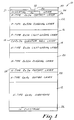
- Fig. 1 is a cross sectional view (not to scale) illustrating the structure of a II-VI semiconductor laser diode in accordance with the present invention.
- Fig. 2 is a schematic illustration of a molecular beam epitaxy system used to fabricate the laser diode shown in Fig. 1.
- Fig. 3 is a graph of the I-V characteristic of sample Au ohmic contacts on p -type ZnSe and similar to that incorporated into the laser diode shown in Fig. 1.
- Fig. 4 is an energy band diagram of an ohmic contact to p -type ZnSe which is similar to that incorporated into the laser diode shown in Fig. 1.
- Fig. 5 is a graph of the measured optical power output from the laser diode shown in Fig. 1 as a function of applied current.
- Fig. 6 1 illustrates a graph of the measured intensity of spontaneous (non-lasing) light output (lower tracing) and a graph of the measured intensity of stimulated (lasing) light output (upper tracing) from the laser diode shown in Fig. 1 as a function of wavelength.
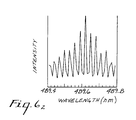
- Fig. 6 2 is a detailed illustration of the central wavelength portion of the upper tracing of Fig. 6 1 .
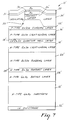
- Fig. 7 is a cross sectional view illustrating the structure of an alternative rib waveguide embodiment of the laser shown in Fig. 1.
- Fig. 8 is a graph of the low-temperature photoluminescence (PL) spectrum of the p -type ohmic contact layer sample similar to that incorporated into the laser diode shown in Fig. 1.
- PL photoluminescence
- Fig. 9 is a diagram of a molecular beam epitaxy chamber for doping semiconductors in accordance with the present invention.
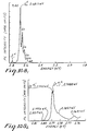
- Figs. 10(a) and 10(b) are graphs of PL intensity versus energy.
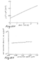
- Fig. 11(a) is a graph of 1/C 2 versus bias voltage for a semiconductor sample described in the Detailed Description Of The Preferred Embodiments.
- Fig. 11(b) is a graph of a net acceptor density versus depletion width for a semiconductor described in the Detailed Description Of The Preferred Embodiments.
- Fig. 12(a) is a cross sectional view (not to scale) of a light emitting diode described in the Detailed Description Of The Preferred Embodiments.
- Fig. 12(b) is a graph of the EL intensity versus wavelength relationship of the light emitting diode shown in Fig. 12(a) at 77K.
- Fig. 13 is a graph of the EL intensity versus wavelength relationship for the light emitting diode shown in Fig. 12(a) at room temperature.
- Fig. 14 is a cross sectional view (not to scale) of a second light emitting diode described in the Detailed Description Of The Preferred Embodiments.
- Laser diode 10 is a wide band gap II-VI device fabricated from heteroepitaxial layers of ZnS x Se 1-x , ZnSe, and Cd y Zn 1-y Se grown by molecular beam epitaxy (MBE) on a GaAs substrate. Prototypes of this device have exhibited laser action, emitting coherent blue-green light near 490 nm from a Cd y Zn 1-y Se quantum well structure under pulsed current injection at 77 K.
- MBE molecular beam epitaxy
- Laser diode 10 is fabricated on a GaAs substrate 12, and includes lower (first) and upper (second) ZnSe light-guiding layers 14 and 16, respectively, separated by a Cd 1-y Zn y Se quantum well active layer 18.
- the surfaces of light-guiding layers 14 and 16 opposite active layer 18 are bounded by lower and upper ZnS x Se 1-x cladding layers 20 and 22, respectively.
- a lower ZnSe ohmic contact layer 24 is positioned on the surface of lower cladding layer 20 opposite light-guiding layer 14, while an upper ZnSe ohmic contact layer 26 is positioned on the surface of upper cladding layer 22 opposite light-guiding layer 16.
- a GaAs buffer layer 28 separates substrate 12 from lower ZnSe contact layer 24 to assure high crystalline quality of the contact and subsequently deposited layers.
- a polyimide insulating layer 34 covers the surface of upper ohmic contact layer 26 opposite upper cladding layer 22. Electrical contact to the ohmic contact layer 26 is made by Au electrode 30 which is formed in a window stripe in insulating layer 34. A thin Ti layer 31 and subsequently a final Au layer 33 are applied over polyimide layer 34 and exposed portions of Au electrode 30 to facilitate lead bonding. Electrical contact to the lower side of laser diode 10 is made by an In electrode 32 on the surface of substrate 12 opposite the lower ohmic contact layer 24.
- Layers 24, 20 and 14 are all doped n -type with Cl (ie., are of a first conductivity type) in prototypes of laser diode 10.
- Layers 16, 22 and 26 are all doped p -type with N (ie., are of a second conductivity type).
- Active layer 18 is an undoped quantum well layer of Cd 0.2 Zn 0.8 Se semiconductor deposited to a thickness of 0.01 ⁇ m.
- Light-guiding layers 14 and 16 are both 0.5 ⁇ m thick. Lower light-guiding layer 14 is doped to a net donor concentration of 1x10 17 cm -3 , while upper light-guiding layer 16 is doped to a net acceptor concentration of 2x10 17 cm -3 .
- Cladding layers 20 and 22 are layers of ZnS 0.07 Se 0.93 semiconductor deposited to thicknesses of 2.5 ⁇ m and 1.5 ⁇ m, respectively.
- the net donor concentration of the lower cladding layer is 1x10 18 cm -3 .
- the net acceptor concentration of the upper cladding layer is 2x10 17 cm -3 .
- Ohmic contact layers 24 and 26 are both deposited to a thickness of 0.1 ⁇ m in these prototype devices.
- the lower contact layer is doped n -type to a net donor concentration of 1x10 18 cm -3 .
- the upper contact layer is doped p -type to a net acceptor concentration of 1x10 18 cm -3 .
- the thicknesses of layers 24, 20, 14, 16, 22 and 26 can be varied as needed for given applications. Typical thickness ranges for contact, cladding and light-guiding layers are 0.03 to 1.0 ⁇ m, 0.5 to 5.0 ⁇ m, and 0.1 to 1.0 ⁇ m, respectively. In general, the thicknesses of light-guiding layers 14 and 16 should be chosen to minimize the width of the optical mode. If the layers 14 and 16 are too thin, the evanescent tails will extend far into cladding layers 20 and 22. Cladding layers 20 and 22 must be thick enough to make absorption of the optical mode in substrate 12 and electrode 32 negligible.
- composition of the Cd x Zn 1-x Se (which determines the laser wavelength) with x of approximately 0.2 was selected to provide a large enough band gap difference ( ⁇ E g of approximately 0.2 eV) to facilitate effective carrier confinement. Larger x will provide deeper quantum wells, but would require a thinner layer due to increased lattice mismatch, thereby decreasing the efficiency of the collection of carriers into the well.
- composition of the ZnS y Se 1-y with y of approximately 0.07 was selected to provide sufficient difference in refractive index from the index of the ZnSe guiding layers to form a low-loss waveguide.
- This composition also provides excellent morphology since it is nearly lattice matched to the GaAs substrate at the growth temperature of 300° C.
- n -type dopants which may be used include Ga, Al, In, I, F, and Br. Oxygen or Li acceptors can also be used for the p -type dopants.
- Other Group V p -type dopants which might be used include arsenic and phosphorous. Greater donor and acceptor concentrations can also be used, although they should not be so high as to cause excessive free-carrier absorption.
- GaAs buffer layer 28 is deposited to a thickness of 1 ⁇ m in this embodiment, and doped n + with Si to a net donor concentration of 1x10 18 cm -3 .
- Other appropriate substrates eg., ZnSe, GaInAs or Ge
- buffer layers such as AlGaAs, AlAs, GaInP, AlInP, AlInAs or GaInAs can also be used.
- the thickness of buffer layer 28 can also be varied while providing an appropriate high-quality surface for growing the II-VI semiconductors. If an appropriate high-quality substrate and appropriate surface preparation is used, buffer layer 28 may not be needed.
- the lattice constants of the ZnSSe cladding layers 20 and 22 and the adjacent ZnSe layers 24, 14 and 16, 26, respectively, are mismatched by about 0.3%.
- Preliminary transmission electron microscopy (TEM) studies indicate that the ZnSe of light-guiding layers 14 and 16 is at least partially relaxed by dislocations formed at the interfaces of the light-guiding layers and the adjacent ZnSSe cladding layers 20 and 22, respectively.
- These preliminary studies also indicate that the thickness of the CdZnSe quantum well active layer 18 is less than the critical thickness for this material system. Quantum well active layer 18 is therefore pseudomorphic, minimizing dislocations in the light-emitting region of laser diode 10.
- the maximum pseudomorphic thicknesses for strained epitaxial layers such as 18 depends on the composition and can be calculated from formulae described in Matthews et al., Defects In Epitaxial Multilayers, J. Crystal Growth, vol. 27, p. 118 (1974).
- quantum well layer 18 which could also be a pseudomorphic layer of other semiconductor material such as ZnSeTe, facilitates the low threshold current operation of laser diode 10 when positioned within the thicker, low-loss II-VI waveguide.
- the waveguide can be made with higher refractive index light-guiding layers 14 and 16 and lower refractive index cladding layers 20 and 22 which can have a relatively small difference in their band gaps and need not be exactly lattice matched.
- the composition of the light-guiding layers may be graded to minimize dislocations and/or to form a graded index waveguide.
- FIG. 2 is an illustration of a molecular beam epitaxy (MBE) system 50 used to fabricate the laser diode 10 described above.
- MBE system 50 includes two MBE chambers 52 and 54 interconnected by ultrahigh vacuum (UHV) pipeline 56. Each chamber 52 and 54 includes a high energy electron gun 58, a phosphorus screen 60, a substrate heater 90 and a flux monitor 62. MBE chambers such as 52 and 54 are generally known and commercially available.
- a Perkin-Elmer Model 430 MBE system was used to produce the prototype laser diodes 10.
- MBE chamber 52 is used to grow the GaAs buffer layer 28 on substrate 12 and includes a Ga effusion cell 64 and an As cracking cell 66.
- a Si effusion cell 68 is also provided as a source of n -type dopants.
- Substrate 12 is cleaned and prepared using conventional or otherwise known techniques, and mounted to a Molybdenum sample block (not shown in Fig. 2) by In solder before being positioned within chamber 52.
- substrate preparation techniques described in the Cheng et al. article Molecular-Beam Epitaxy Growth Of ZnSe Using A Cracked Selenium Source, J. Vac. Sci. Technol., B8, 181 (1990) were used to produce the prototype laser diode 10.
- the Si doped buffer layer 28 can be grown on substrate 12 by operating MBE chamber 52 in a conventional manner, such as that described in Technology and Physics of Molecular Beam Epitaxy, ed. E.H.C. Parker, Plenum Press, 1985.
- the resulting buffer layer 28 has an As-rich surface which exhibited a c(4x4) reconstruction as observed by reflection high energy electron diffraction (RHEED).
- RHEED reflection high energy electron diffraction
- chamber 54 includes a Zn effusion cell 70, cracked-Se effusion cell 72, ZnS effusion cell 74 (as a source of S), Cd effusion cell 76 and a standard Se (ie., primarily Se 6 ) effusion cell 79.
- cracked-Se effusion cell 72 includes a bulk evaporator 84 and high temperature cracking zone 82, and provides a source of cracked Se (including Se 2 and other Se molecules with less than 6 atoms).
- the bulk evaporator 84 and high temperature cracking zone 82 used to produce the prototype laser diodes 10 are of a custom design, the details and capabilities of which are described in the Cheng et al. J. Vac. Sci. Technol. article referenced above.
- Cl effusion cell 78 which utilizes ZnCl 2 source material provides the Cl n -type dopant.
- the p -type dopant is provided by N free-radical source 80.
- Free-radical source 80 is connected to a source 86 of ultra-pure N 2 through leak-valve 88.
- the free-radical source 80 used in the fabrication of laser diodes 10 is commercially available from Oxford Applied Research Ltd. of Oxfordshire, England (Model No. MPD21).
- This source has a length of 390 mm.
- the beam exit plate at the end of the source is made of pyrolytic boron nitride (PBN) and has nine 0.2 mm diameter holes through it.
- PBN pyrolytic boron nitride
- This source is mounted on a standard port for an effusion cell through a 10" extension tube.
- N 2 source 86 used to fabricate laser diodes 10 is of research purity grade, produced by Matheson Gas Products.
- the pressure at the inlet of the leak-valve of source 86 is 5 psi.
- MBE chamber 54 is operated in a manner described in the Cheng et al. article Growth Of p- and n-Type ZnSe By Molecular Beam Epitaxy, J. Crystal Growth 95, 512 (1989) using the Se 6 source 79 as the source of Se to grow the n -type contact, cladding and light-guiding layers 24, 20 and 14, respectively, of the prototype laser diode 10.
- Quantum well active layer 18 is grown in a manner described in the Samarth et al. article, Molecular Beam Epitaxy of CdSe and the Derivative Alloys Zn 1-x Cd x Se and Cd 1-x Mn x Se, J . Electronic Materials, vol. 19. No. 6, p. 543 (1990).
- MBE chamber 54 is operated in a manner described in the copending Park et al. U.S. Patent Application Serial Number 07/573,428, entitled Doping Of IIB-VIA Semiconductors During Molecular Beam Epitaxy and filed on August 24, 1990, using the Se 6 source 79 to grow the p -type light-guiding layer 16 and cladding layer 22.
- the disclosure contained in the above-referenced U.S. Patent Application Serial Number 07/573,428 is reproduced immediately below.
- An atomic dopant beam (either nitrogen or oxygen), produced by a free-radical source, is used to dope ZnSe during molecular beam epitaxy which produces p-type ZnSe epitaxial thin films.
- electromagnetic power at the frequency of 13.52 MHz is coupled to an RF plasma discharge chamber of the free-radical source, atomic dopant species are generated inside the chamber of the free-radical source from a gaseous source of ultra-high purity.
- a diffuser plate having 18 holes of about 0.3 mm diameter each was used to separate the free-radical source and the molecular beam epitaxy chamber.
- the amount of the atomic dopant species generated is controlled by the level of the RF power coupled to, and the pressure in the RF plasma discharge chamber.
- the atomic dopant species, which effuse into the molecular beam epitaxy chamber through openings in the diffuser plate, are used as the dopants during the molecular beam epitaxy growth of ZnSe.
- ZnSe thin layers are grown on a well-polished GaAs surface with the surface normal vector essentially along the [001] crystal orientation.
- GaAs substrate available from, for example, Sumitomo Electric Industries, Ltd., 1-1 Koyakita 1-Chome, Itami, Hyogo, 664 Japan, or the GaAs epitaxial layer, available from Spire Corporation, Patriots Park, Bedford, Massachusetts, 01730, for this purpose.
- the GaAs substrates are degreased in trichloroethane, acetone, and isopropanol, rinsed in deionized water and blown dry by high purity nitrogen gas.
- the degreased substrates are chemically etched in a solution consisting of six parts of sulfuric acid, one part of hydrogen peroxide and one part of deionized water for several minutes (about two to five minutes).
- the substrate is rinsed in deionized water and blown dry by high purity nitrogen gas.
- the degreased and chemically-etched GaAs substrates are then attached to a Mo sample block using molten In of high purity as solder.
- the substrate assembly is immediately loaded into the molecular beam epitaxy system.
- the GaAs substrates are heated in the ultra-high vacuum growth chamber to about 610°C for about one to five minutes to desorb the native oxides and expose the underlying crystalline structure on which the ZnSe with the same crystal structure is to be grown.
- the typical growth conditions for ZnSe by molecular beam epitaxy are a Zn to Se beam equivalent pressure ratio of 1:2 (in the range of about 1:4 to 2:1) and a growth temperature of 275°C (in the range of about 250°C to 400°C).
- Typical layer thicknesses and growth rates are 2 ⁇ m and 0.5 ⁇ m/h (in the range of about 0.4 ⁇ m/h to 2.0 ⁇ m/h) respectively.
- the atomic dopants generated by the free-radical source are incorporated into the ZnSe by opening the mechanical shutter which blocks the line of sight path between the free-radical source and the heated substrates.
- the present invention utilizes a method and apparatus for the in-situ production of epitaxial structures comprising ZnSe pn junctions. This is useful in the fabrication of efficient light-emitting devices, such as light-emitting diodes and diode lasers which operate in the blue region of the visible spectrum.
- Either nitrogen or oxygen are an excellent p-type dopant element in ZnSe.
- nitrogen and oxygen are stable in ZnSe at temperatures up to 375°C.
- Fig. 9 shows a molecular beam epitaxy system 110.
- Molecular beam epitaxy system 110 includes a molecular beam epitaxy chamber 112 which encloses a substrate 114.
- Molecular beam epitaxy chamber 112 includes an electron gun 116, a phosphorus screen 118 and a flux monitor 120.
- Effusion cells 122, 124, 126, and 128 are carried in molecular beam epitaxy chamber 112.
- Effusion cells 122, 124, 126, and 128 may comprise, for example, effusion cells for Zn, Se, and ZnCl 2 .
- Molecular beam epitaxy system 10 also includes a free-radical source 130.
- Free-radical source 130 may comprise a source of any group VA or oxygen free-radicals.
- free-radical source 130 may provide a source of nitrogen free-radicals, in which free-radical source 130 is supplied with ultra-pure N 2 from an ultra-pure N 2 source 132 through a valve 133.
- Free-radical source 130 is available from Oxford Applied Research Ltd. (Oxfordshire, UK).
- Free-radical source 130 might comprise other types of sources which produce free-radicals.
- an electron cyclotron resonance (ECR) free-radical source may be used (available from, for example, Wavemat, Inc., 44780 Helm Street, Plymouth, Michigan).
- ECR electron cyclotron resonance
- a microwave cracker coupled into the gas source through a microwave tube may be used to produce free-radicals.
- a DC plasma discharge chamber may also be used.
- any appropriate thermal cracker or disassociation cell available from, for example, EPI, 261 East Fifth Street, St. Paul, Minnesota 55101 may be used.
- ZnSe layers were grown on GaAs substrates in a molecular beam epitaxy system of the type described herein. These layers were grown at a substrate temperature of 275°C with a Zn to Se beam equivalent pressure ratio of 1:2 (typical layer thicknesses and growth rates were 2 ⁇ m and 0.5 ⁇ m/h, respectively).
- P-type doping of the ZnSe layers was achieved by a free-radical source which was incorporated in the molecular beam epitaxy system, rather than a conventional effusion source.
- the free-radical source provided a flux of atomic nitrogen (together with a much larger flux of non-dissociated N 2 ) created in a RF plasma discharge chamber.
- a RF frequency of 13.5 MHz was used to generate nitrogen atoms from a gaseous source of ultra-pure N 2 .
- the atomic nitrogen flux level was controlled by suitably adjusting the intensity of the RF plasma discharge.
- Net acceptor concentrations, N A -N D , in the nitrogen doped ZnSe/GaAs layers were determined using capacitance-voltage (C-V) profiling. Since the ZnSe epitaxial layers were grown on semi-insulating GaAs, planar profiling between two Schottky contacts on the ZnSe surface was carried out.
- the surface contact pattern consisted of a series of 762 ⁇ m diameter Cr/Au dots physically isolated from a large Cr/Au surrounding electrode. The separation between the inner (dot) electrodes and the outer electrode was 25 ⁇ m, a small separation being necessary in order to maintain a low series resistance.
- the contact pattern was created by thermally evaporating 75 ⁇ of Cr followed by 1000 ⁇ of Au and performing photolithographic and lift-off processes. In all of these measurements the outer electrode was held at ground potential and bias was applied to the inner Schottky contact.
- Figs. 11(a) and 11(b) The 1/C 2 versus V plot and the N A -N D versus depletion width profile obtained from a heavily-doped ZnSe layer are illustrated in Figs. 11(a) and 11(b), respectively.
- the material is p-type with a net acceptor concentration around 3.4x10 17 cm -3 .
- Fig. 11(a) and 11(b) the material is p-type with a net acceptor concentration around 3.4x10 17 cm -3 .
- the doping profile is rather flat from zero bias (0.068 ⁇ m) out to where reverse bias breakdown occurs (1.126 ⁇ m). Breakdown occurred at 3.8 V which is consistent with avalanche breakdown in ZnSe material doped at this level, ie, 3.4x10 17 cm -3 p-type.
- Fig. 12(a) shows a light emitting diode 134.
- Light emitting diode 134 includes a p-type GaAs substrate 136.
- P-type GaAs substrate 136 forms the base for molecular beam epitaxial growth.
- a p-type ZnSe nitrogen doped layer 138 is deposited upon p-type GaAs substrate 136.
- P-type ZnSe layer 138 is deposited in accordance with the present invention using a nitrogen free-radical source.
- An n-type ZnSe chlorine doped layer 140 is deposited upon p-type ZnSe layer 138.
- An n + ZnSe cap layer 142 is deposited upon n-type ZnSe layer 140.
- n + ZnSe cap layer 142 has a thickness of 2 ⁇ m and has a net acceptor concentration of 1x10 17 cm -3 .
- N-type ZnSe layer 140 has a thickness of 0.5 ⁇ m and a net donor concentration of 1x10 18 cm -3 .
- the n + ZnSe cap layer 142 has a thickness of 500 ⁇ and a net donor concentration of 5x10 18 cm -3 .
- Fig. 12(a) shows the p-type ZnSe layer is grown first on a p + -type GaAs substrate.
- This type of "buried p-type layer" structure avoids the serious problems associated with ohmic contact formation to p-type ZnSe (See M.A. Haase, H. Cheng, J.M. DePuydt, and J.E. Potts, J. Appl. Phys., 67, 448 (1990)).
- a disadvantage with this device design is that a large hole barrier exists at the p + -GaAs/p-ZnSe hetero-interface (see L. Kassel, H. Abad, J.W. Garland, P.M.
- Light-emitting diode fabrication was accomplished using conventional photolithographic techniques with device isolation being achieved by wet chemical etching to form 400 ⁇ m diameter mesas.
- the top electrode metalization was ring shaped and was patterned by vacuum evaporation and lift-off. Ultrasonic gold ball bonding was used to make contact to the devices for electroluminescence characterization.
- FIG. 12(b) A typical electroluminescence spectrum recorded at 77K for light emitting diode 134 shown in Fig. 12(a), is illustrated in Fig. 12(b).
- the device operating voltage and current were 13.5 V and 40 mA, respectively, for the spectrum shown in Fig. 12(a).
- the visible electroluminescence is dominated by blue emission, the spectrum comprising a number of resolved lines principally at 447.7 nm, 459.6 nm and 464.7 nm.
- FIG. 13 An electroluminescence spectrum recorded at room temperature from the device structure illustrated in Fig. 12(a) (visible region only) is shown in Fig. 13. As can be seen from the figure, dominant emission in the blue region of the visible spectrum is observed, peaking in intensity at a wavelength of 465 nm. For the particular spectrum shown in Fig. 13, the voltage applied and current drawn were 22 V and 20 mA, respectively.
- Fig. 14 shows a light emitting diode 148.
- Light emitting diode 148 is a p on n device which operates similar to light emitting diode 134 of Fig. 12(a).
- Light emitting diode 148 includes an n + GaAs substrate 150, an n-type ZnSe layer 152 and p-type ZnSe layer 154.
- Contacts 156 and 158 make electrical contact with p-type ZnSe layer 154 and n + GaAs substrate 150.
- the p-type ZnSe layer 154 is deposited using molecular beam epitaxy and a group VA free-radical source described above.
- n-type ZnSe layer 152 has a net donor concentration of about 1x10 18 cm -3 and a thickness of about 2.0 ⁇ m and p-type ZnSe layer 154 has a net acceptor concentration of about 1x10 17 cm -3 and a thickness of 0.5 ⁇ m.
- n-type IIB-VIA semiconductor film may also be produced.
- the resultant IIB-VIA semiconductor film may be used in pn junction devices such as light emitting diodes and light detectors as well as diode lasers and transistors.
- the free-radical source is introduced into a molecular beam epitaxy growth chamber to provide a dopant to a IIB-VIA semiconductor during molecular beam epitaxial growth.
- the free-radical source may be nitrogen, phosphorus, arsenic, and antimony. Oxygen may also be used as a suitable free-radical source.
- the method and apparatus may be used for N-doping and O-doping of ZnSe.
- P-type ternary IIB-VIA semiconductors including Zn 1-x Cd x Se, ZnSe 1- x Te x , ZnSe 1-x S x , ZnS 1-x Te x , and Zn 1-x Cd x S.
- lower ZnSSe cladding layer 20 is doped n-type using the ZnCl 2 source.
- Other aspects of the techniques used to grow cladding layers 20 and 22 are described in the Matsumura et al. article, Optimum Composition In MBE-ZnS x Se 1-x /Znse For High Quality Heteroepitaxial Growth, J. Crys. Growth, vol. 99, p. 446 (1990).
- a low resistivity p -type ZnSe ohmic contact layer 26 has been achieved by growing the contact layer at low temperature within MBE chamber 54 utilizing the cracked Se source 72 (ie., cracking zone 82 and evaporator 84), while at the same time doping the semiconductor material of the contact layer p -type in accordance with the method described above.
- the low temperature growth technique used to produce the contact layer 26 of the prototype laser diode 10 is described generally in the Cheng et al. article Low Temperature Growth Of ZnSe By Molecular Beam Epitaxy Using Cracked Selenium, Appl. Phys. Lett. (Feb. 1990).
- the semiconductor body with layers 28, 24, 20, 14, 18, 16 and 22 on substrate 12 is heated to a temperature less than 250° C but high enough to promote crystalline growth of the ZnSe doped with the N p -type dopants to a net acceptor concentration of at least 1x10 17 cm -3 .
- a net acceptor concentration of 1x10 18 cm -3 was achieved in the ohmic contact layer 26 of prototype laser diodes 10, when grown at a substrate temperature of about 150° C.
- ohmic contact layers 26 with acceptable characteristics can be achieved at other growth temperatures down to at least 130° C.
- MBE chamber 54 used to produce the ohmic contact layer 26 of the prototype laser diodes 10 are as follows: Zn beam equivalent pressure: 1.0x10 -7 Torr* Se cracking zone temperature: 600° C* Se bulk evaporator temperature: 250° C* Growth rate: 0.3-0.6 ⁇ m/hr Surface reconstruction: Zn-stabilized Nitrogen pressure in chamber: >3.5x10 -7 Torr* rf power: 150-250 W* * parameters dependant upon specific MBE system configuration
- Figure 3 is the current-voltage characteristic of a sample with two coplanar Au metal electrodes on a p -type ZnSe contact layer produced for test purposes in a manner substantially similar to that described above. The ohmic nature of this contact is indicated by the substantially linear nature of the curve over the -6 to +6 volt range.
- FIG. 4 is an energy band diagram of the Au - p -type ZnSe contact layer interface.
- additional electronic energy states 102 are formed in the contact layer. These additional energy states 102 are relatively deep (within the forbidden gap) with respect to the valence band maximum, compared to the depth of the shallow impurity level 100. Energy states 102 are in effect intermediate energy states located at an energy less than the Au Fermi level and greater than the shallow impurity level 100.
- additional energy states 102 greatly increase the tunneling probability by providing a temporary residence for the carriers and facilitate multi-step or cascade tunneling.
- E F is the Fermi energy
- E A is the acceptor energy.
- a diagramatic depiction of an electron making a multi-step tunneling transfer between the ZnSe and Au layers through the additional energy states 102 is also shown in Figure 4. Even better contacts are attainable with electronic states at more than one energy level, such that tunneling can occur from state to state across the barrier.
- additional energy states 102 can be achieved by a number of methods. Doping during growth, diffusion, ion implantation or other known techniques can be used to incorporate impurities which produce deep levels.
- impurities which produce deep levels.
- One important type of deep level impurity is the iso-electronic trap.
- Te is thought to form a hole trap in ZnSe.
- the additional energy states 102 can also be achieved by introducing proper native crystal defects such as, but not limited to, dislocations, vacancies, interstitials or complexes into contact layer 26. This can be done during the deposition of the contact layer by choosing the molecular species of the precursors, and/or by other appropriate growth conditions.
- Native defects can also be generated by post-growth treatments such as irradiation by electron beams, ion beams, radical beams or electromagnetic radiation. However, these techniques must be implemented without detrimentally degrading the conductivity of the ZnSe or other semiconductor material used for the contact layer.
- the useful p -type contact layer 26 has a number of properties.
- the net acceptor density N A -N D is large, preferrably at least 1x10 18 cm -3 . This serves to reduce the width of the barrier through which the charge carriers must tunnel.
- the p -type dopant concentration (nitrogen in laser diode 10) must also be large, preferrably at least 1x10 19 cm -3 .
- the nitrogen impurities also appear to participate in the formation of the deep energy states. At a minimum, the amount of nitrogen required is that which will provide adequate concentrations of both types of levels.
- the growth conditions must also be appropriate to form the defects at the energy levels described above. The low temperature growth technique described above has been shown to produce these material properties (contact resistances less than 0.4 ohm-cm 2 have been achieved).
- the low-temperature photoluminescence (PL) spectrum from a good ohmic contact layer such as 26 is shown in Figure 8.
- the observed characteristics include: 1) the very weak near band edge PL; 2) the appearance of the defect band at 2.3 eV (18,500 cm -1 ); and 3) the presence of a band (presumably associated with donor-acceptor-pair recombination) at about 2.5 eV (20,400 cm -1 ).
- the band edge PL is expected to be weak for materials which have significant concentrations of deep levels since the deep levels provide long wavelength and nonradiative channels which compete with the near band edge processes.
- the emission band at approximately 2.3 eV is associated with a transition from the conduction band to a deep (acceptor) level about 0.5 eV above the valence band maximum.
- the emission band at 2.5 eV is believed to be related to transitions from donor to acceptor states. No or minimal donor states would be preferrable, eliminating this transition, or shifting its occurance to slightly higher energies.
- Electrode 30 includes Au which is vacuum evaporated onto contact layer 26 and patterned into a stripe (typically about 20 ⁇ m wide) using conventional photolithography and lift-off. An insulating layer 34 of is then applied over electrode 30 and the exposed surface of contact layer 26. For an insulator that can be applied at low temperatures, polyimide photoresist is preferred. Probimide 408 from Ciba-Geigy Corp. was used to produce laser diode 10.
- a stripe (about 20 ⁇ m wide) of the polyimide layer 34 directly above electrode 30 is removed by UV exposure through a photomask and development using the manufacturer's recommended processing recipe, except for the post-development cure.
- the device was flood exposed to 1 J/cm 2 of UV light from a mask aligner, and baked at 125° C on a hot plate in air for 3 minutes.
- Ti-Au layer 31 is then evaporated on the exposed surface of the Au electrode 30 and polyimide layer 34 to facilitate lead-bonding.
- the In used for MBE substrate bonding also served as electrode 32 on substrate 12.
- Opposite ends of the device were cleaved along (110) planes to form facet mirrors. Cavity length of the prototype devices 10 is about 1000 ⁇ m. Laser diodes 10 were then bonded p -side up to ceramic sample holders with silver-filled epoxy.
- index-guided laser 10' such as that shown in Figure 7.
- Index-guided laser 10' is similar to laser 10 and can be fabricated with the same II-VI semiconductor layers. Portions of laser 10' which correspond to those of laser 10 are indicated with identical but primed (ie., "X"') reference numerals.
- laser 10' includes a waveguide or rib 35 in the cladding layer 22' and contact layer 26'. Rib 35 can be formed to a width of about 5 ⁇ m by ion beam etching with a Xe or Ar ion beam or by wet-chemical etching.
- Conventional photoresist can be used as a mask for this process.
- Other known and conventional techniques can also be used to provide lateral waveguiding. These techniques include using substrates in which grooves have been etched (ie., channelled-substrate lasers), or etching a rib and regrowing a top cladding layer (ie., a "buried heterostructure" laser). Improvements in the threshold current or the differential quantum efficiency may be achieved by dielectric coatings of the facets to adjust the reflectivities.
- Initial tests of the prototype laser diodes 10 were conducted at 77 K by pulsing the devices, typically with 500 nsec pulses and a 500 ⁇ sec period. Current measurements were made with a box-car averager, while a large Si photodetector was used to collect and monitor the output light intensity from one end facet of the device. The measured light output as a function of current (ie., L-I) characteristics from one of the devices is illustrated in Figure 5.
- the threshold current is 74 mA, which corresponds to a threshold current density of 320 A/cm 2 . Differential quantum efficiencies in excess of 20% per facet have been measured, as have pulsed output powers of over 100 mW per facet.
- the coherent light is strongly TE polarized and a "speckle pattern" is clearly visible.
- the output laser beam has an elliptical far-field pattern, with a divergence of roughly 40°x4° for the central lobe. Side lobes are visible, indicating higher order transverse modes.
- the measured L-I characteristics do indicate some dependence on pulse length.
- the gain in the single quantum well prototype devices tends to saturate.
- the index of refraction is reduced due to the injection of excess carriers, which tends to make the region under the stripe of electrode 30 anti-guiding.
- Thermal effects become important at these current densities, as thermal gradients and the temperature dependence of the index provide lateral optical confinement. It is expected that these characteristics will be alleviated by index-guided versions such as laser diode 10'.
- Figures 6 1 and 6 2 are graphs of the optical spectra that are characteristic of the prototype laser diodes 10 at 77 K.
- the spectra illustrated in Figures 6 1 and 6 2 were acquired using a SPEX 1403 double monochromator.
- the spontaneous emission occurs at 490 nm and has a FWHM of about 3 nm.
- the 1060 ⁇ m long device operates in many longitudinal modes centered at 489.6 ⁇ m, and which are separated by 0.03 nm.
- the operating voltage of the prototype laser diodes 10 at the threshold current is approximately 15 V. This characteristic indicates that there is still room for improvement in the ohmic contact between electrode 30 and contact layer 26 and/or improvement in the conductivity of p -type layers 16, 22, and 26. Reducing this series resistance and improving the heat-sinking of the device (ie., by solder-bonding the p -type side down) are expected to facilitate CW operation at higher temperatures.
- the concepts disclosed herein and used to fabricate the prototype laser diode 10 are equally well suited to the fabrication of laser diodes from a wide variety of other compound II-VI semiconductor alloys, especially from other ZnSe alloys.
- improved operating characterisics will be achieved by using lattice matched materials such as Cd x Zn 1-x S (with x of approximately 0.61) and ZnSe to form the waveguide.
- the quantum well in such a device may include CdZnSe.
- This semiconductor system will not suffer from misfit dislocations which can decrease efficiency and the useful lifetime of the devices.
- a multiple quantum well active layer made of a strained-layer superlattice could replace the single pseudomorphic quantum well layer 18.
- Ohmic contact layer 26 might also be improved by using thin layers of smaller band gap II-VI alloys such as ZnSe 1-x Te x , Cd x Zn 1-x Se and Hg x Zn 1-x Se.
- Group VI sources other than Se 2 can also be used to produce ohmic contacts in accordance with the present invention.
- Other metals (eg., Pt) or other electrically conductive materials having a large work function (eg., >5eV) and suitable for a stable semiconductor interface can also be used as electrodes.
Landscapes
- Physics & Mathematics (AREA)
- Optics & Photonics (AREA)
- Condensed Matter Physics & Semiconductors (AREA)
- General Physics & Mathematics (AREA)
- Electromagnetism (AREA)
- Engineering & Computer Science (AREA)
- Chemical & Material Sciences (AREA)
- Nanotechnology (AREA)
- Biophysics (AREA)
- Life Sciences & Earth Sciences (AREA)
- Crystallography & Structural Chemistry (AREA)
- Semiconductor Lasers (AREA)
- Led Devices (AREA)
- Electrodes Of Semiconductors (AREA)
- Physical Deposition Of Substances That Are Components Of Semiconductor Devices (AREA)
- Luminescent Compositions (AREA)
Claims (11)
- II-VI-Verbundhalbleiter-Laserdiode (10) mit mehreren Schichten aus II-VI-Halbleitermaterial, durch die ein pn-Übergangsbereich gebildet wird, einer innerhalb des pn-Übergangsbereichs angeordneten aktiven Quantenquellenschicht (18) aus II-VI-Halbleitermaterial, einem Halbleitersubstrat (12) zum Halten der Schichten aus II-VI-Halbleitermaterial und einer ersten und einer zweiten Elektrode (32, 33), die an entgegengesetzten Seiten der Schichten aus II-VI-Halbleitermaterial angeordnet sind, um der Laserdiode elektrische Energie zuzuführen;
gekennzeichnet durch eine erste und eine zweite lichtleitende Schicht (14, 16) aus II-VI-Halbleitermaterial innerhalb der Schichten des den pn-Übergangsbereich bildenden II-VI-Halbleitermaterials, wobei die aktive Quantenquellenschicht zwischen der ersten und der zweiten lichtleitenden Schicht angeordnet ist. - Laserdiode nach Anspruch 1, mit:einer zwischen dem Substrat (12) und der ersten lichtleitenden Schicht (14) angeordneten ersten Mantelschicht (20) aus II-VI-Halbleitermaterial eines ersten Leitungstyps; undeiner auf der bezüglich der ersten Mantelschicht (20) entgegengesetzten Seite der ersten lichtleitenden Schicht (14) angeordneten zweiten Mantelschicht (22) aus II-VI-Halbleitermaterial eines zweiten Leitungstyps.
- Laserdiode nach Anspruch 1, wobei die mehreren Schichten aus II-VI-Halbleitermaterial aufweisen:eine auf dem Substrat (12) angeordnete erste lichtleitende Schicht (14) aus II-VI-Halbleitermaterial eines ersten Leitungstyps; undeine auf der ersten lichtleitenden Schicht (14) angeordnete zweite lichtleitende Schicht (16) aus II-VI-Halbleitermaterial eines zweiten Leitungstyps, wobei die erste und die zweite lichtleitende Schicht den pn-Übergang bilden.
- Laserdiode nach Anspruch 3, ferner mit:einer zwischen dem Substrat (12) und der ersten lichtleitenden Schicht (14) angeordneten ersten Mantelschicht (20) aus II-VI-Halbleitermaterial des ersten Leitungstyps; undeiner bezüglich der ersten lichtleitenden Schicht (14) auf der entgegengesetzten Seite der zweiten lichtleitenden Schicht (16) angeordneten zweiten Mantelschicht (22) aus II-VI-Halbleitermaterial des zweiten Leitungstyps.
- Laserdiode nach einem der Ansprüche 1 bis 4, ferner mit einem in mindestens einer der Schichten aus II-VI-Halbleitermaterial ausgebildeten Wellenleitersteg (35).
- Laserdiode nach einem der Ansprüche 1 bis 5, wobei die aktive Schicht (18) eine aktive Quantenquellenschicht aufweist.
- Laserdiode nach einem der Ansprüche 1 bis 6, wobei die aktive Schicht (18) eine aktive Mehrquantenquellenschicht aufweist.
- Laserdiode nach einem der Ansprüche 1 bis 7, wobei die aktive Schicht (18) Zink und Selen aufweist.
- Laserdiode nach einem der Ansprüche 1 bis 8, wobei die aktive Schicht (18) außerdem Cadmium aufweist.
- Laserdiode nach einem der Ansprüche 1 bis 9, wobei mindestens eine p-leitende Schicht aus II-VI-Halbleitermaterial mit p-leitenden Dotierungsstoffen aus einer Quelle freier Radikale in einer Netto-Akzeptorkonzentration von mindestens 1x1017cm-3 dotiert ist.
- Elektronisches System mit einer II-VI-Laserdiode nach einem der Ansprüche 1 bis 10 zum Emittieren eines kohärenten Lichtstrahls im blauen und/oder grünen Bereich des Spektrums.
Priority Applications (1)
| Application Number | Priority Date | Filing Date | Title |
|---|---|---|---|
| EP95108005A EP0670593A3 (de) | 1991-05-15 | 1992-05-12 | II-VI Halbleitervorrichtung und blau-grüner Diodenlaser. |
Applications Claiming Priority (7)
| Application Number | Priority Date | Filing Date | Title |
|---|---|---|---|
| US70060191A | 1991-05-15 | 1991-05-15 | |
| US07/700,606 US5274269A (en) | 1991-05-15 | 1991-05-15 | Ohmic contact for p-type group II-IV compound semiconductors |
| US700580 | 1991-05-15 | ||
| US700601 | 1991-05-15 | ||
| US700606 | 1991-05-15 | ||
| US07/700,580 US5213998A (en) | 1991-05-15 | 1991-05-15 | Method for making an ohmic contact for p-type group II-VI compound semiconductors |
| PCT/US1992/003782 WO1992021170A2 (en) | 1991-05-15 | 1992-05-12 | Blue-green laser diode |
Related Child Applications (1)
| Application Number | Title | Priority Date | Filing Date |
|---|---|---|---|
| EP95108005.0 Division-Into | 1995-05-24 |
Publications (2)
| Publication Number | Publication Date |
|---|---|
| EP0584236A1 EP0584236A1 (de) | 1994-03-02 |
| EP0584236B1 true EP0584236B1 (de) | 1997-07-16 |
Family
ID=27418708
Family Applications (2)
| Application Number | Title | Priority Date | Filing Date |
|---|---|---|---|
| EP92912423A Expired - Lifetime EP0584236B1 (de) | 1991-05-15 | 1992-05-12 | Blau-gruen diodenlaser |
| EP95108005A Withdrawn EP0670593A3 (de) | 1991-05-15 | 1992-05-12 | II-VI Halbleitervorrichtung und blau-grüner Diodenlaser. |
Family Applications After (1)
| Application Number | Title | Priority Date | Filing Date |
|---|---|---|---|
| EP95108005A Withdrawn EP0670593A3 (de) | 1991-05-15 | 1992-05-12 | II-VI Halbleitervorrichtung und blau-grüner Diodenlaser. |
Country Status (15)
| Country | Link |
|---|---|
| EP (2) | EP0584236B1 (de) |
| JP (1) | JP3269558B2 (de) |
| KR (1) | KR100247682B1 (de) |
| CN (2) | CN1097317C (de) |
| AU (1) | AU654726B2 (de) |
| BR (1) | BR9205993A (de) |
| CA (1) | CA2109310C (de) |
| DE (1) | DE69220942T2 (de) |
| ES (1) | ES2104931T3 (de) |
| FI (1) | FI110971B (de) |
| IL (1) | IL101857A (de) |
| MY (2) | MY110622A (de) |
| RU (1) | RU2127478C1 (de) |
| SG (1) | SG46466A1 (de) |
| WO (1) | WO1992021170A2 (de) |
Cited By (1)
| Publication number | Priority date | Publication date | Assignee | Title |
|---|---|---|---|---|
| CN102185060A (zh) * | 2011-04-15 | 2011-09-14 | 映瑞光电科技(上海)有限公司 | 一种氮化物led结构及其制备方法 |
Families Citing this family (42)
| Publication number | Priority date | Publication date | Assignee | Title |
|---|---|---|---|---|
| US5396103A (en) * | 1991-05-15 | 1995-03-07 | Minnesota Mining And Manufacturing Company | Graded composition ohmic contact for P-type II-VI semiconductors |
| US5341001A (en) * | 1992-02-13 | 1994-08-23 | Matsushita Electric Industrial Co., Ltd. | Sulfide-selenide manganese-zinc mixed crystal photo semiconductor and laser diode |
| JP3453787B2 (ja) * | 1993-06-18 | 2003-10-06 | ソニー株式会社 | 半導体レーザ及びその製造方法 |
| MY111898A (en) * | 1993-07-02 | 2001-02-28 | Sony Corp | Semiconductor laser |
| US5640409A (en) * | 1993-07-02 | 1997-06-17 | Sony Corporation | Semiconductor laser |
| US5422902A (en) * | 1993-07-02 | 1995-06-06 | Philips Electronics North America Corporation | BeTe-ZnSe graded band gap ohmic contact to p-type ZnSe semiconductors |
| JPH07231142A (ja) * | 1994-02-18 | 1995-08-29 | Mitsubishi Electric Corp | 半導体発光素子 |
| JPH07263372A (ja) * | 1994-03-24 | 1995-10-13 | Sharp Corp | Ii−vi族化合物半導体装置およびその製造方法 |
| US5442204A (en) * | 1994-05-12 | 1995-08-15 | Philips Electronics North America Corporation | III-V Semiconductor heterostructure contacting a P-type II-VI compound |
| US6876003B1 (en) | 1999-04-15 | 2005-04-05 | Sumitomo Electric Industries, Ltd. | Semiconductor light-emitting device, method of manufacturing transparent conductor film and method of manufacturing compound semiconductor light-emitting device |
| PL202938B1 (pl) * | 2000-02-16 | 2009-08-31 | Nichia Corp | Azotkowe półprzewodnikowe urządzenie laserowe |
| DE10260183A1 (de) * | 2002-12-20 | 2004-07-15 | Osram Opto Semiconductors Gmbh | Vertikal emittierender, optisch gepumpter Halbleiterlaser mit externem Resonator |
| JP4085953B2 (ja) * | 2003-10-22 | 2008-05-14 | 住友電気工業株式会社 | 半導体光素子 |
| CN100477300C (zh) * | 2003-10-27 | 2009-04-08 | 洲磊科技股份有限公司 | 形成光电元件的方法 |
| JP4411540B2 (ja) * | 2005-09-15 | 2010-02-10 | ソニー株式会社 | 半導体レーザ装置 |
| DE112011101530B4 (de) * | 2010-04-30 | 2021-03-25 | Trustees Of Boston University | Verfahren zur Herstellung einer optischen Vorrichtung |
| CN102185058B (zh) * | 2011-04-02 | 2013-09-25 | 映瑞光电科技(上海)有限公司 | 一种氮化物led结构及其制备方法 |
| WO2013163347A1 (en) | 2012-04-25 | 2013-10-31 | Rockwell Collins, Inc. | Holographic wide angle display |
| US9933684B2 (en) | 2012-11-16 | 2018-04-03 | Rockwell Collins, Inc. | Transparent waveguide display providing upper and lower fields of view having a specific light output aperture configuration |
| WO2014188149A1 (en) | 2013-05-20 | 2014-11-27 | Milan Momcilo Popovich | Holographic waveguide eye tracker |
| EP3245444B1 (de) | 2015-01-12 | 2021-09-08 | DigiLens Inc. | Umweltisolierte wellenleiteranzeige |
| WO2016113533A2 (en) | 2015-01-12 | 2016-07-21 | Milan Momcilo Popovich | Holographic waveguide light field displays |
| US9632226B2 (en) | 2015-02-12 | 2017-04-25 | Digilens Inc. | Waveguide grating device |
| CN113759555B (zh) | 2015-10-05 | 2024-09-20 | 迪吉伦斯公司 | 波导显示器 |
| EP3548939A4 (de) | 2016-12-02 | 2020-11-25 | DigiLens Inc. | Wellenleitervorrichtung mit gleichmässiger ausgabebeleuchtung |
| WO2018129398A1 (en) | 2017-01-05 | 2018-07-12 | Digilens, Inc. | Wearable heads up displays |
| US10732569B2 (en) | 2018-01-08 | 2020-08-04 | Digilens Inc. | Systems and methods for high-throughput recording of holographic gratings in waveguide cells |
| US20190212588A1 (en) | 2018-01-08 | 2019-07-11 | Digilens, Inc. | Systems and Methods for Manufacturing Waveguide Cells |
| KR20250004154A (ko) | 2018-01-08 | 2025-01-07 | 디지렌즈 인코포레이티드. | 광 도파관의 제조 방법 |
| WO2020149956A1 (en) | 2019-01-14 | 2020-07-23 | Digilens Inc. | Holographic waveguide display with light control layer |
| US20200247017A1 (en) | 2019-02-05 | 2020-08-06 | Digilens Inc. | Methods for Compensating for Optical Surface Nonuniformity |
| US20220283377A1 (en) | 2019-02-15 | 2022-09-08 | Digilens Inc. | Wide Angle Waveguide Display |
| DE102019205376B4 (de) | 2019-04-15 | 2024-10-10 | Forschungszentrum Jülich | Herstellen eines ohmschen Kontakts sowie elektronisches Bauelement mit ohmschem Kontakt |
| CN114207492A (zh) | 2019-06-07 | 2022-03-18 | 迪吉伦斯公司 | 带透射光栅和反射光栅的波导及其生产方法 |
| JP7207365B2 (ja) * | 2019-06-19 | 2023-01-18 | 株式会社デンソー | 半導体レーザ光源モジュール、半導体レーザ装置 |
| KR102775783B1 (ko) | 2019-08-29 | 2025-02-28 | 디지렌즈 인코포레이티드. | 진공 격자 및 이의 제조 방법 |
| EP4288831A4 (de) | 2021-03-05 | 2025-01-15 | Digilens Inc. | Evakuierte periodische strukturen und herstellungsverfahren |
| DE102021004609A1 (de) | 2021-09-11 | 2023-03-16 | Eques Consulting GmbH | Vorrichtung und damit durchführbares Verfahren zur non-invasiven Konzentrationsbestimmung von Komponenten im menschlichen Blutkreislauf und Verwendung des Verfahrens. |
| CN114665382A (zh) * | 2022-03-23 | 2022-06-24 | 海南师范大学 | 高效散热深刻蚀双沟道脊形量子级联激光器及制造方法 |
| CN115247979B (zh) * | 2022-06-08 | 2024-10-25 | 天津电力机车有限公司 | 一种应用于复合式散热器高级修的预防性维修方法 |
| CN115498077B (zh) * | 2022-09-22 | 2024-09-06 | 深圳市思坦科技有限公司 | 红光微型led芯片制备方法、红光微型led芯片以及显示装置 |
| CN119108897B (zh) * | 2024-07-29 | 2025-11-18 | 安徽格恩半导体有限公司 | 一种具有激子极化子拓扑层的半导体激光器 |
Family Cites Families (12)
| Publication number | Priority date | Publication date | Assignee | Title |
|---|---|---|---|---|
| JPS5863183A (ja) * | 1981-10-09 | 1983-04-14 | Semiconductor Res Found | 2−6族間化合物の結晶成長法 |
| JPS598383A (ja) * | 1982-07-06 | 1984-01-17 | Semiconductor Res Found | ZnSe緑色発光ダイオ−ド |
| JPH0728052B2 (ja) * | 1986-01-27 | 1995-03-29 | 株式会社東芝 | 半導体発光素子およびその製造方法 |
| JPS63185077A (ja) * | 1987-01-27 | 1988-07-30 | Matsushita Electric Ind Co Ltd | 青色発光ダイオ−ド |
| DE3810245A1 (de) * | 1987-03-27 | 1988-10-06 | Japan Incubator Inc | Lichtemittierendes element und verfahren zu seiner herstellung |
| JPS63288072A (ja) * | 1987-05-20 | 1988-11-25 | Seiko Epson Corp | 半導体発光装置 |
| JPH01140663A (ja) * | 1987-11-27 | 1989-06-01 | Toshiba Corp | 半導体装置の電極 |
| JPH01184977A (ja) * | 1988-01-20 | 1989-07-24 | Inkiyuubeetaa Japan:Kk | 可視発光半導体レーザ装置 |
| US4992837A (en) * | 1988-11-15 | 1991-02-12 | Kokusai Denshin Denwa Co., Ltd. | Light emitting semiconductor device |
| US5081632A (en) * | 1989-01-26 | 1992-01-14 | Hitachi, Ltd. | Semiconductor emitting device |
| US5028561A (en) * | 1989-06-15 | 1991-07-02 | Hughes Aircraft Company | Method of growing p-type group II-VI material |
| US5248631A (en) * | 1990-08-24 | 1993-09-28 | Minnesota Mining And Manufacturing Company | Doping of iib-via semiconductors during molecular beam epitaxy using neutral free radicals |
-
1992
- 1992-05-12 KR KR1019930703441A patent/KR100247682B1/ko not_active Expired - Fee Related
- 1992-05-12 AU AU20264/92A patent/AU654726B2/en not_active Ceased
- 1992-05-12 CA CA002109310A patent/CA2109310C/en not_active Expired - Fee Related
- 1992-05-12 ES ES92912423T patent/ES2104931T3/es not_active Expired - Lifetime
- 1992-05-12 BR BR9205993A patent/BR9205993A/pt not_active IP Right Cessation
- 1992-05-12 EP EP92912423A patent/EP0584236B1/de not_active Expired - Lifetime
- 1992-05-12 EP EP95108005A patent/EP0670593A3/de not_active Withdrawn
- 1992-05-12 SG SG1996004919A patent/SG46466A1/en unknown
- 1992-05-12 DE DE69220942T patent/DE69220942T2/de not_active Expired - Fee Related
- 1992-05-12 WO PCT/US1992/003782 patent/WO1992021170A2/en not_active Ceased
- 1992-05-12 RU RU93058663A patent/RU2127478C1/ru not_active IP Right Cessation
- 1992-05-12 JP JP50007793A patent/JP3269558B2/ja not_active Expired - Fee Related
- 1992-05-14 MY MYPI92000817A patent/MY110622A/en unknown
- 1992-05-14 IL IL10185792A patent/IL101857A/en not_active IP Right Cessation
- 1992-05-14 MY MYPI95003142A patent/MY111574A/en unknown
- 1992-05-15 CN CN92103575A patent/CN1097317C/zh not_active Expired - Fee Related
- 1992-05-15 CN CNB021479372A patent/CN1321488C/zh not_active Expired - Fee Related
-
1993
- 1993-11-12 FI FI935022A patent/FI110971B/fi not_active IP Right Cessation
Non-Patent Citations (2)
| Title |
|---|
| (Toyko, JP), Y. KAWAKAMI et al.: "Optically pumped blue-green laser operation above room-temperature in Zn0.80Cd0.20Se-ZnS0.08Se0.92 multiple quantum well structures grown by metalorganic molecular beam epitaxy", pages L605-L607 * |
| M. PARK et al.: "P-type ZnSe by nitrogen atom beam doping during molecular beam epitaxial growth", pages 2127-2129 * |
Cited By (2)
| Publication number | Priority date | Publication date | Assignee | Title |
|---|---|---|---|---|
| CN102185060A (zh) * | 2011-04-15 | 2011-09-14 | 映瑞光电科技(上海)有限公司 | 一种氮化物led结构及其制备方法 |
| CN102185060B (zh) * | 2011-04-15 | 2014-07-16 | 映瑞光电科技(上海)有限公司 | 一种氮化物led结构及其制备方法 |
Also Published As
| Publication number | Publication date |
|---|---|
| WO1992021170A2 (en) | 1992-11-26 |
| WO1992021170A3 (en) | 1993-03-04 |
| AU654726B2 (en) | 1994-11-17 |
| ES2104931T3 (es) | 1997-10-16 |
| JPH06508003A (ja) | 1994-09-08 |
| FI935022A7 (fi) | 1993-11-12 |
| KR100247682B1 (ko) | 2000-03-15 |
| AU2026492A (en) | 1992-12-30 |
| MY111574A (en) | 2000-08-30 |
| EP0584236A1 (de) | 1994-03-02 |
| IL101857A0 (en) | 1992-12-30 |
| CA2109310A1 (en) | 1992-11-16 |
| DE69220942T2 (de) | 1998-03-05 |
| MY110622A (en) | 1998-09-30 |
| CA2109310C (en) | 2001-10-02 |
| CN1321488C (zh) | 2007-06-13 |
| CN1066936A (zh) | 1992-12-09 |
| BR9205993A (pt) | 1994-08-02 |
| EP0670593A3 (de) | 1996-02-07 |
| CN1097317C (zh) | 2002-12-25 |
| HK1001353A1 (en) | 1998-06-12 |
| FI935022A0 (fi) | 1993-11-12 |
| CN1474485A (zh) | 2004-02-11 |
| SG46466A1 (en) | 1998-02-20 |
| JP3269558B2 (ja) | 2002-03-25 |
| RU2127478C1 (ru) | 1999-03-10 |
| FI110971B (fi) | 2003-04-30 |
| EP0670593A2 (de) | 1995-09-06 |
| IL101857A (en) | 1998-12-06 |
| DE69220942D1 (de) | 1997-08-21 |
Similar Documents
| Publication | Publication Date | Title |
|---|---|---|
| CA2109310C (en) | Blue-green laser diode | |
| US5291507A (en) | Blue-green laser diode | |
| US5404027A (en) | Buried ridge II-VI laser diode | |
| US5274269A (en) | Ohmic contact for p-type group II-IV compound semiconductors | |
| EP0793281B1 (de) | Elektromagnetische Umwandler | |
| US7101444B2 (en) | Defect-free semiconductor templates for epitaxial growth | |
| US5213998A (en) | Method for making an ohmic contact for p-type group II-VI compound semiconductors | |
| EP0683924B1 (de) | Verfahren zur Herstellung eines p-leitenden ohmschen Kontakts mit variabler Zusammensetzung für p-Typ II-VI Halbleiter | |
| US5513199A (en) | Blue-green laser diode | |
| US5508522A (en) | Method for producing a group II-VI compound semiconductor thin film and a group II-VI compound semiconductor device | |
| US5818859A (en) | Be-containing II-VI blue-green laser diodes | |
| RU2151457C1 (ru) | Способ изготовления омического контактного слоя и полупроводниковое устройство ii-vi групп | |
| HK1001353B (en) | Blue-green laser diode | |
| CA2234517A1 (en) | Blue-green lase diode | |
| HK1002373B (en) | Electro-magnetic transducers |
Legal Events
| Date | Code | Title | Description |
|---|---|---|---|
| PUAI | Public reference made under article 153(3) epc to a published international application that has entered the european phase |
Free format text: ORIGINAL CODE: 0009012 |
|
| 17P | Request for examination filed |
Effective date: 19931111 |
|
| AK | Designated contracting states |
Kind code of ref document: A1 Designated state(s): BE CH DE ES FR GB IT LI NL |
|
| 17Q | First examination report despatched |
Effective date: 19940330 |
|
| GRAG | Despatch of communication of intention to grant |
Free format text: ORIGINAL CODE: EPIDOS AGRA |
|
| GRAH | Despatch of communication of intention to grant a patent |
Free format text: ORIGINAL CODE: EPIDOS IGRA |
|
| GRAH | Despatch of communication of intention to grant a patent |
Free format text: ORIGINAL CODE: EPIDOS IGRA |
|
| GRAA | (expected) grant |
Free format text: ORIGINAL CODE: 0009210 |
|
| AK | Designated contracting states |
Kind code of ref document: B1 Designated state(s): BE CH DE ES FR GB IT LI NL |
|
| XX | Miscellaneous (additional remarks) |
Free format text: TEILANMELDUNG 95108005.0 EINGEREICHT AM 12/05/92. |
|
| REG | Reference to a national code |
Ref country code: CH Ref legal event code: EP |
|
| REF | Corresponds to: |
Ref document number: 69220942 Country of ref document: DE Date of ref document: 19970821 |
|
| ET | Fr: translation filed | ||
| REG | Reference to a national code |
Ref country code: ES Ref legal event code: FG2A Ref document number: 2104931 Country of ref document: ES Kind code of ref document: T3 |
|
| REG | Reference to a national code |
Ref country code: CH Ref legal event code: NV Representative=s name: E. BLUM & CO. PATENTANWAELTE |
|
| PLBE | No opposition filed within time limit |
Free format text: ORIGINAL CODE: 0009261 |
|
| STAA | Information on the status of an ep patent application or granted ep patent |
Free format text: STATUS: NO OPPOSITION FILED WITHIN TIME LIMIT |
|
| 26N | No opposition filed | ||
| REG | Reference to a national code |
Ref country code: GB Ref legal event code: IF02 |
|
| PGFP | Annual fee paid to national office [announced via postgrant information from national office to epo] |
Ref country code: FR Payment date: 20060517 Year of fee payment: 15 |
|
| PGFP | Annual fee paid to national office [announced via postgrant information from national office to epo] |
Ref country code: NL Payment date: 20060524 Year of fee payment: 15 |
|
| PGFP | Annual fee paid to national office [announced via postgrant information from national office to epo] |
Ref country code: ES Payment date: 20060526 Year of fee payment: 15 |
|
| PGFP | Annual fee paid to national office [announced via postgrant information from national office to epo] |
Ref country code: CH Payment date: 20060530 Year of fee payment: 15 |
|
| PGFP | Annual fee paid to national office [announced via postgrant information from national office to epo] |
Ref country code: IT Payment date: 20060531 Year of fee payment: 15 |
|
| PGFP | Annual fee paid to national office [announced via postgrant information from national office to epo] |
Ref country code: BE Payment date: 20060620 Year of fee payment: 15 |
|
| PGFP | Annual fee paid to national office [announced via postgrant information from national office to epo] |
Ref country code: DE Payment date: 20070702 Year of fee payment: 16 |
|
| REG | Reference to a national code |
Ref country code: CH Ref legal event code: PFA Owner name: MINNESOTA MINING AND MANUFACTURING COMPANY Free format text: MINNESOTA MINING AND MANUFACTURING COMPANY#3M CENTER, P.O. BOX 33427#ST. PAUL, MINNESOTA 55133-3427 (US) -TRANSFER TO- MINNESOTA MINING AND MANUFACTURING COMPANY#3M CENTER, P.O. BOX 33427#ST. PAUL, MINNESOTA 55133-3427 (US) |
|
| PGFP | Annual fee paid to national office [announced via postgrant information from national office to epo] |
Ref country code: GB Payment date: 20070525 Year of fee payment: 16 |
|
| BERE | Be: lapsed |
Owner name: *MINNESOTA MINING AND MFG CY Effective date: 20070531 |
|
| REG | Reference to a national code |
Ref country code: CH Ref legal event code: PL |
|
| PG25 | Lapsed in a contracting state [announced via postgrant information from national office to epo] |
Ref country code: NL Free format text: LAPSE BECAUSE OF NON-PAYMENT OF DUE FEES Effective date: 20071201 |
|
| NLV4 | Nl: lapsed or anulled due to non-payment of the annual fee |
Effective date: 20071201 |
|
| PG25 | Lapsed in a contracting state [announced via postgrant information from national office to epo] |
Ref country code: LI Free format text: LAPSE BECAUSE OF NON-PAYMENT OF DUE FEES Effective date: 20070531 Ref country code: CH Free format text: LAPSE BECAUSE OF NON-PAYMENT OF DUE FEES Effective date: 20070531 |
|
| REG | Reference to a national code |
Ref country code: FR Ref legal event code: ST Effective date: 20080131 |
|
| PG25 | Lapsed in a contracting state [announced via postgrant information from national office to epo] |
Ref country code: BE Free format text: LAPSE BECAUSE OF NON-PAYMENT OF DUE FEES Effective date: 20070531 |
|
| PG25 | Lapsed in a contracting state [announced via postgrant information from national office to epo] |
Ref country code: FR Free format text: LAPSE BECAUSE OF NON-PAYMENT OF DUE FEES Effective date: 20070531 |
|
| REG | Reference to a national code |
Ref country code: ES Ref legal event code: FD2A Effective date: 20070514 |
|
| PG25 | Lapsed in a contracting state [announced via postgrant information from national office to epo] |
Ref country code: ES Free format text: LAPSE BECAUSE OF NON-PAYMENT OF DUE FEES Effective date: 20070514 |
|
| GBPC | Gb: european patent ceased through non-payment of renewal fee |
Effective date: 20080512 |
|
| PG25 | Lapsed in a contracting state [announced via postgrant information from national office to epo] |
Ref country code: DE Free format text: LAPSE BECAUSE OF NON-PAYMENT OF DUE FEES Effective date: 20081202 |
|
| PG25 | Lapsed in a contracting state [announced via postgrant information from national office to epo] |
Ref country code: GB Free format text: LAPSE BECAUSE OF NON-PAYMENT OF DUE FEES Effective date: 20080512 |
|
| PG25 | Lapsed in a contracting state [announced via postgrant information from national office to epo] |
Ref country code: IT Free format text: LAPSE BECAUSE OF NON-PAYMENT OF DUE FEES Effective date: 20070512 |