EP0584833B1 - Filière en diamant et procédé pour la fabrication de cette filière - Google Patents
Filière en diamant et procédé pour la fabrication de cette filière Download PDFInfo
- Publication number
- EP0584833B1 EP0584833B1 EP93113751A EP93113751A EP0584833B1 EP 0584833 B1 EP0584833 B1 EP 0584833B1 EP 93113751 A EP93113751 A EP 93113751A EP 93113751 A EP93113751 A EP 93113751A EP 0584833 B1 EP0584833 B1 EP 0584833B1
- Authority
- EP
- European Patent Office
- Prior art keywords
- diamond
- synthesized
- wire drawing
- layer
- drawing die
- Prior art date
- Legal status (The legal status is an assumption and is not a legal conclusion. Google has not performed a legal analysis and makes no representation as to the accuracy of the status listed.)
- Expired - Lifetime
Links
Images



Classifications
-
- C—CHEMISTRY; METALLURGY
- C23—COATING METALLIC MATERIAL; COATING MATERIAL WITH METALLIC MATERIAL; CHEMICAL SURFACE TREATMENT; DIFFUSION TREATMENT OF METALLIC MATERIAL; COATING BY VACUUM EVAPORATION, BY SPUTTERING, BY ION IMPLANTATION OR BY CHEMICAL VAPOUR DEPOSITION, IN GENERAL; INHIBITING CORROSION OF METALLIC MATERIAL OR INCRUSTATION IN GENERAL
- C23C—COATING METALLIC MATERIAL; COATING MATERIAL WITH METALLIC MATERIAL; SURFACE TREATMENT OF METALLIC MATERIAL BY DIFFUSION INTO THE SURFACE, BY CHEMICAL CONVERSION OR SUBSTITUTION; COATING BY VACUUM EVAPORATION, BY SPUTTERING, BY ION IMPLANTATION OR BY CHEMICAL VAPOUR DEPOSITION, IN GENERAL
- C23C16/00—Chemical coating by decomposition of gaseous compounds, without leaving reaction products of surface material in the coating, i.e. chemical vapour deposition [CVD] processes
- C23C16/01—Chemical coating by decomposition of gaseous compounds, without leaving reaction products of surface material in the coating, i.e. chemical vapour deposition [CVD] processes on temporary substrates, e.g. substrates subsequently removed by etching
-
- B—PERFORMING OPERATIONS; TRANSPORTING
- B21—MECHANICAL METAL-WORKING WITHOUT ESSENTIALLY REMOVING MATERIAL; PUNCHING METAL
- B21C—MANUFACTURE OF METAL SHEETS, WIRE, RODS, TUBES, PROFILES OR LIKE SEMI-MANUFACTURED PRODUCTS OTHERWISE THAN BY ROLLING; AUXILIARY OPERATIONS USED IN CONNECTION WITH METAL-WORKING WITHOUT ESSENTIALLY REMOVING MATERIAL
- B21C3/00—Profiling tools for metal drawing; Combinations of dies and mandrels for metal drawing
- B21C3/02—Dies; Selection of material therefor; Cleaning thereof
-
- B—PERFORMING OPERATIONS; TRANSPORTING
- B21—MECHANICAL METAL-WORKING WITHOUT ESSENTIALLY REMOVING MATERIAL; PUNCHING METAL
- B21C—MANUFACTURE OF METAL SHEETS, WIRE, RODS, TUBES, PROFILES OR LIKE SEMI-MANUFACTURED PRODUCTS OTHERWISE THAN BY ROLLING; AUXILIARY OPERATIONS USED IN CONNECTION WITH METAL-WORKING WITHOUT ESSENTIALLY REMOVING MATERIAL
- B21C3/00—Profiling tools for metal drawing; Combinations of dies and mandrels for metal drawing
- B21C3/02—Dies; Selection of material therefor; Cleaning thereof
- B21C3/025—Dies; Selection of material therefor; Cleaning thereof comprising diamond parts
-
- C—CHEMISTRY; METALLURGY
- C23—COATING METALLIC MATERIAL; COATING MATERIAL WITH METALLIC MATERIAL; CHEMICAL SURFACE TREATMENT; DIFFUSION TREATMENT OF METALLIC MATERIAL; COATING BY VACUUM EVAPORATION, BY SPUTTERING, BY ION IMPLANTATION OR BY CHEMICAL VAPOUR DEPOSITION, IN GENERAL; INHIBITING CORROSION OF METALLIC MATERIAL OR INCRUSTATION IN GENERAL
- C23C—COATING METALLIC MATERIAL; COATING MATERIAL WITH METALLIC MATERIAL; SURFACE TREATMENT OF METALLIC MATERIAL BY DIFFUSION INTO THE SURFACE, BY CHEMICAL CONVERSION OR SUBSTITUTION; COATING BY VACUUM EVAPORATION, BY SPUTTERING, BY ION IMPLANTATION OR BY CHEMICAL VAPOUR DEPOSITION, IN GENERAL
- C23C16/00—Chemical coating by decomposition of gaseous compounds, without leaving reaction products of surface material in the coating, i.e. chemical vapour deposition [CVD] processes
- C23C16/22—Chemical coating by decomposition of gaseous compounds, without leaving reaction products of surface material in the coating, i.e. chemical vapour deposition [CVD] processes characterised by the deposition of inorganic material, other than metallic material
- C23C16/26—Deposition of carbon only
- C23C16/27—Diamond only
-
- C—CHEMISTRY; METALLURGY
- C23—COATING METALLIC MATERIAL; COATING MATERIAL WITH METALLIC MATERIAL; CHEMICAL SURFACE TREATMENT; DIFFUSION TREATMENT OF METALLIC MATERIAL; COATING BY VACUUM EVAPORATION, BY SPUTTERING, BY ION IMPLANTATION OR BY CHEMICAL VAPOUR DEPOSITION, IN GENERAL; INHIBITING CORROSION OF METALLIC MATERIAL OR INCRUSTATION IN GENERAL
- C23C—COATING METALLIC MATERIAL; COATING MATERIAL WITH METALLIC MATERIAL; SURFACE TREATMENT OF METALLIC MATERIAL BY DIFFUSION INTO THE SURFACE, BY CHEMICAL CONVERSION OR SUBSTITUTION; COATING BY VACUUM EVAPORATION, BY SPUTTERING, BY ION IMPLANTATION OR BY CHEMICAL VAPOUR DEPOSITION, IN GENERAL
- C23C16/00—Chemical coating by decomposition of gaseous compounds, without leaving reaction products of surface material in the coating, i.e. chemical vapour deposition [CVD] processes
- C23C16/22—Chemical coating by decomposition of gaseous compounds, without leaving reaction products of surface material in the coating, i.e. chemical vapour deposition [CVD] processes characterised by the deposition of inorganic material, other than metallic material
- C23C16/26—Deposition of carbon only
- C23C16/27—Diamond only
- C23C16/271—Diamond only using hot filaments
-
- Y—GENERAL TAGGING OF NEW TECHNOLOGICAL DEVELOPMENTS; GENERAL TAGGING OF CROSS-SECTIONAL TECHNOLOGIES SPANNING OVER SEVERAL SECTIONS OF THE IPC; TECHNICAL SUBJECTS COVERED BY FORMER USPC CROSS-REFERENCE ART COLLECTIONS [XRACs] AND DIGESTS
- Y10—TECHNICAL SUBJECTS COVERED BY FORMER USPC
- Y10T—TECHNICAL SUBJECTS COVERED BY FORMER US CLASSIFICATION
- Y10T428/00—Stock material or miscellaneous articles
- Y10T428/24—Structurally defined web or sheet [e.g., overall dimension, etc.]
- Y10T428/24273—Structurally defined web or sheet [e.g., overall dimension, etc.] including aperture
-
- Y—GENERAL TAGGING OF NEW TECHNOLOGICAL DEVELOPMENTS; GENERAL TAGGING OF CROSS-SECTIONAL TECHNOLOGIES SPANNING OVER SEVERAL SECTIONS OF THE IPC; TECHNICAL SUBJECTS COVERED BY FORMER USPC CROSS-REFERENCE ART COLLECTIONS [XRACs] AND DIGESTS
- Y10—TECHNICAL SUBJECTS COVERED BY FORMER USPC
- Y10T—TECHNICAL SUBJECTS COVERED BY FORMER US CLASSIFICATION
- Y10T428/00—Stock material or miscellaneous articles
- Y10T428/24—Structurally defined web or sheet [e.g., overall dimension, etc.]
- Y10T428/24273—Structurally defined web or sheet [e.g., overall dimension, etc.] including aperture
- Y10T428/24281—Struck out portion type
-
- Y—GENERAL TAGGING OF NEW TECHNOLOGICAL DEVELOPMENTS; GENERAL TAGGING OF CROSS-SECTIONAL TECHNOLOGIES SPANNING OVER SEVERAL SECTIONS OF THE IPC; TECHNICAL SUBJECTS COVERED BY FORMER USPC CROSS-REFERENCE ART COLLECTIONS [XRACs] AND DIGESTS
- Y10—TECHNICAL SUBJECTS COVERED BY FORMER USPC
- Y10T—TECHNICAL SUBJECTS COVERED BY FORMER US CLASSIFICATION
- Y10T428/00—Stock material or miscellaneous articles
- Y10T428/24—Structurally defined web or sheet [e.g., overall dimension, etc.]
- Y10T428/24942—Structurally defined web or sheet [e.g., overall dimension, etc.] including components having same physical characteristic in differing degree
-
- Y—GENERAL TAGGING OF NEW TECHNOLOGICAL DEVELOPMENTS; GENERAL TAGGING OF CROSS-SECTIONAL TECHNOLOGIES SPANNING OVER SEVERAL SECTIONS OF THE IPC; TECHNICAL SUBJECTS COVERED BY FORMER USPC CROSS-REFERENCE ART COLLECTIONS [XRACs] AND DIGESTS
- Y10—TECHNICAL SUBJECTS COVERED BY FORMER USPC
- Y10T—TECHNICAL SUBJECTS COVERED BY FORMER US CLASSIFICATION
- Y10T428/00—Stock material or miscellaneous articles
- Y10T428/30—Self-sustaining carbon mass or layer with impregnant or other layer
Definitions
- the present invention relates to a diamond wire drawing die and a diamond plate, especially one made of gaseous phase synthetic diamond.
- Diamond has the greatest hardness and highest modulus of elasticity of all known materials. Furthermore, extremely pure diamond has the highest thermal conductivity and the highest transmittance in the infrared spectrum. Thus, diamond is a material for which there are no comparative substitutes.
- a method of synthesizing diamond from a gaseous phase is disclosed in U.S. Patent No. 4,767,608 issued August 30, 1988 to Matsumoto, et al. Furthermore, U.S. Patent No. 4,434,188 issued February 28, 1984 to Kamo et al discloses synthesizing diamond from a gaseous phase.
- Concerning a wire drawing die a polycrystalline diamond composite is disclosed in U.S. Patent No. 3,831,428 issued August 27, 1974 H. Wentorf. Jr.
- a composite wire drawing die construction is described in which a centrally-located mass of diamond defines at least the throat of the wire drawing hole, the mass being flanked or girded by at least one mass of metal bonded carbide that is directly bonded thereto.
- EP-0,391,418-A1 relates to a diamond wire drawing die made of synthesized single crystal diamond provided by the temperature gradient method, and it describes a method of producing wire drawing dies by cleaving diamond.
- a drawing die is a tool used, for example, for drawing a metal wire, it is required to have properties as follows:
- Diamond which has these properties, is a superior raw material for a wire drawing die.
- a natural single crystal diamond, synthesized single crystal diamond and a poly crystalline diamond composite were used for a central portion of the wire drawing die.
- the natural single crystal diamond and the synthesized single crystal diamond are expensive and have faults such as limitation of crystal size and they are easy to cleave and prone to breakage.
- the polycrystalline diamond composite in spite of overcoming the faults of single crystal diamonds, has additional faults relating to wear and heat resistance because it contains sintering aids.
- a diamond wire drawing die is known from EP-A-0 494 799, which comprises a single layer of a gaseous phase synthesised polycrystalline diamond having a preferred orientation, the grain size being from under 1 ⁇ m to over tens of ⁇ m.
- Another object of the present invention is to provide a diamond wire drawing die in which the hole is made substantially perpendicular to the bonding surface.
- Another object of the present invention is to provide a diamond wire drawing die in which the hole is substantially parallel to the bonding surface and the bonding surface is located substantially in the central portion of the hole.
- Another object of the present invention is to provide a method to produce such a diamond wire drawing die.
- the disclosed process for manufacturing a diamond wire drawing die comprises the following:
- the other process for manufacturing a diamond wire drawing die is different from the above process in die hole direction.
- the die hole is parallel to the bonding surface and the bonding surface is located substantially in the central portion of the hole.
- Fig.1 is a schematic process diagram for making a central portion of the diamond wire drawing die according to a preferred embodiment of the present invention.
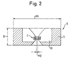
- Fig.2 is a schematic cross sectional view of the diamond wire drawing die which was made in example 1.
- Fig.3 is a schematic process diagram for making a central portion of the diamond wire drawing die which was made in example 2.
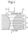
- Fig.4 is a schematic cross sectional view of the internal structure at the die hole portion of a diamond wire drawing die.
- Fig.5 shows a particle size distribution obtained in Example 3.
- Fig.4 is schematic cross sectional view of the internal structure at the die hole portion of a diamond wire drawing die according to a prior technique.
- the internal structure at the hole portion (15) of the central portion (14) of a diamond wire drawing die consists of an entrance portion (16), a reduction portion (17) and an exit portion (18).
- the entrance portion (16) consists of a so-called entrance part or a bell part (19) and an approach part (20).
- the so-called entrance part or the bell part (19) is the entrance for wire (21) to be drawn, and is provided to allow lubricant to easily flow into the hole.
- the approach part (20) is provided to inhibit wire vibration, to fix the wire to be drawn, and to allow lubricant to easily flow into the hole.
- the reduction portion (17) consists of a reduction part (22) and a bearing part (23).
- the reduction part (22) reduces the wire (21) to be drawn, and is an important part because it influences the property of a wire drawing die and the quality of the drawn wire.
- the bearing part (23) influences the diameter and surface roughness of the drawn wire (21).
- the exit portion (18) consists of a back-relief part (24) and an exit part (25).
- the back-relief part (24) reinforces the bearing part (23) during wire (21) drawing.
- the exit part (25) is responsible for threading the hole with the fine tip of the wire (21) before drawing.
- the wire (21) to be drawn is threaded into the entrance portion (16).
- the wire (21) contacts the reduction portion (17) and is plastically deformed into a desired shape, diameter and surface roughness and is then drawn away from the exit portion (18).
- the wire (21) is reduced in diameter and improved in physical properties such as yield strength and surface roughness during these drawing processes.
- the reduction portion of the wire drawing die is constructed by a comparatively large particle of columner structure diamond, which grows during gaseous phase synthesizing, there is a possibility of cleaving the same as a single crystal diamond, and its strength is insufficient to allow it to utilize a diamond made by a gaseous phases.
- the fine nuclei develop in the initial stage and then grow to form a film.
- the particle size in the initial stage is remarkably influenced by previous substrate treatment and synthesizing conditions, it is possible to synthesize a diamond having a diameter of not more than 0.5 ⁇ m. Therefore, a high performance of the diamond wire drawing die is expected when a small particle portion is formed at the reduction portion.
- a diamond has a suitable structure for the wire drawing die.
- the inventive diamond is obtained by the following process; a first polycrystalline diamond layer is initially synthesized on a substrate and then the substrate is removed, a second polycrystalline diamond layer is further synthesized on the first polycristalline diamond layer's surface such that its synythesizing direction is opposite that of the first diamond layer.
- the diamond wire drawing die of the present invention comprises; a wire contact portion which is a diamond synthesized by a gaseous phase method and a reduction portion of the wire drawing die which constitutes the finest structure of the diamond.
- the method of manufacturing the diamond wire drawing die of the present invention comprises; a process to synthesize the first polycrystalline diamond layer on a substrate by a gaseous phase method, a process to remove the substrate, a process to synthesize the second polycrystalline diamond layer on the first polycrystalline diamond layer's surface to which the substrate adhered before being removed, a process to make a die hole penetrating the first and the second polycrystalline diamond layers so that the hole crosses the bonding surface of the first and second polycrystalline diamond layers.
- the method of manufacturing the diamond wire drawing die of the present invention comprises; a process to synthesize the first polycrystalline diamond layer on a substrate by a gaseous phase method, a process to remove the substrate, a process to synthesize the second polycrystalline diamond layer on the first polycrystalline diamond layer's surface to which the substrate adhered before removal, a process to make a die hole penetrating in a direction parallel to the bonding surface of the first and the second polycrystalline diamond layers so that the bonding surface is substantially in the central portion of die hole and the hole penetrates the first and the second polycrystalline diamond layers.
- the diamond wire drawing die of the present invention comprises the diamond synthesized by a gaseous phase method which contacts the wire to be drawn.
- This diamond material produced by the gaseous phase method has a fine structure and also consists only of diamond, therefore it has superior wear, heat and chipping resistance as compared to a polycrystalline diamond composite.
- the diamond produced by the gaseous phase method has a fine structure at the initial stage of diamond growth on a substrate and has a tendency to develop a more columner structure and a larger particle size.
- the diamond wire drawing die of the present invention is made by this process; after synthesizing the first polycrystalline diamond layer on a substrate by the gaseous phase method, the substrate is removed, and the second polycrystalline diamond layer is then synthesized on the first polycrystalline layer's surface to which the substrate adhered before the substrate was removed. Therefore, the diamond wire drawing die has finer diamond crystals near the bonding surface of the first and the second polycrystalline diamond layers than other portions. The greater the distance from the bonding surface, the larger is the diamond crystals.
- the diamond wire drawing die of the present invention Since the portion which has fine diamond crystals at the bonding surface of the first and the second polycrystalline diamond forms the reduction portion of a die hole, the diamond wire drawing die of the present invention has a hard and cleaving-resistant die hole. Therefore the diamond wire drawing die has superior wear resistance because the die hole is scarcely scarred by exfoliated diamonds.
- tungsten and molybdenum wire are drawn at a high temperature to improve plasticity.
- higher drawing temperatures shorten the die life.
- a polycrystalline diamond composite contains binder material, it has inferior heat resistance.
- a gaseous phase synthesized diamond is superior to the polycrystalline diamond composite in terms of heat resistance because the gaseous phase synthesized diamond does not contain the binder material and has nearly the same heat conductivity as a natural diamond.
- non-diamond ingredient in the gaseous phase synthesized diamond remarkably reduces wear resistance, it is desirable to decrease the amount of non diamond ingredient to as little as possible.
- Fig.1 is a schematic process diagram for making a diamond wire drawing die according to a preferred embodiment of the present invention.
- Cross-sectional views shown in each step (101) ⁇ (105) of Fig.1 schematically show the crystal structure of gaseous phase synthesized diamond which is used for the present invention. The higher the line density and the shorter line length, the finer the crystal structure the portion has in each cross sectional view.
- the process of the wire drawing die in the present invention is explained using Fig.1.
- the first polycrystalline diamond layer (2) was synthesized on a substrate (1) by the gaseous phase synthesizing method shown at step (101).
- the first polycrystalline diamond layer (2) was synthesized to 500 ⁇ m in thickness on a Si substrate (1) by hot filament CVD.
- the synthesizing condition is shown in Table 1.
- the substrate (1) was removed in step (102).
- the Si substrate with the first polycrystalline diamond layer (2) was dipped in hydrofluoric-nitric acid to remove the Si substrate.
- the second polycrystalline diamond layer (4) was synthesized by the gaseous phase synthesizing method on the first polycrystalline diamond layer's surface which is the same surface as that to which the Si substrate adhered to the first polycrystalline diamond layer before removal.
- a multilayer (5) is formed.
- the second polycrystalline diamond layer (4) was synthesized to 500 ⁇ m in thickness on the side (3) of the first polycrystalline diamond layer by hot filament CVD. The synthesizing was carried out under the same conditions as the first polycrystalline diamond layer (2).
- a multilayer (5) is formed into a central portion (7) having a desired shape and size so that the bonding surface (6) between the first polycrystalline diamond layer (2) and the second polycrystalline diamond layer (4) is horizontal.
- the central portion (7) is processed by laser machining.
- a die hole (8) is formed in the central portion. The die hole (8) is made through the first polycrystalline diamond layer and the second polycrystalline diamond layer across the bonding surface (6) of the first polycrystalline diamond layer and the second polycrystalline diamond layer by laser machining and ultrasonic machining in the central portion (7).
- the central portion (7) of diamond wire drawing die provided by the above steps is made of diamond produced by the gaseous phase synthesizing method and the reduction portion (8S) of the die hole (8) penetrating the multilayer diamond has the finest structure in the multilayer polycrystalline diamond.
- a diamond wire drawing die of which a cross sectional view is shown in Fig.2, is provided using the central portion (7) having a die hole (8).
- the diamond wire drawing die (9) comprises the central portion (7), a reinforcing mount material (10) and the case (11).
- the central portion (7) is bonded to the reinforcing mount material (10) and the reinforcing material (10) is brazed to the case (11).
- Fig.3 shows a schematic diagram of the steps used to produce the diamond wire drawing die of the preferred embodiment of the present invention.
- the process of making the inventive diamond wire drawing die is explained. Since the process of example 2, shown in Fig.3, is the same as the process of example 1, shown in Fig.1, except for steps (104) and (105), the same reference signs represent the same parts as in Fig.1 and are not explained further.
- the difference between the process of example 2, shown in Fig.3, and the process of example 1, shown in Fig.1, is that the central portion (12) is formed into a desired shape and size so that the bonding surface of the first polycrystalline diamond layer and the second polycrystalline diamond layer is vertical.
- a die hole (13) in the multilayer is formed in a direction parallel to the bonding surface of the first polycrystalline diamond layer (2) and the second polycrystalline diamond layer (4) so that the center of the die hole is located near the bonded surface.
- the central portion (12) of the wire drawing die formed by the above process consists of diamond which is synthesized by the gaseous phase synthesizing method and the reduction portion (13S) in the die hole (13) has the finest polycrystalline diamond structure as clearly shown in Fig.3.
- the size and the shape of the hole portion (13) are the same as in example 1.
- the central portion (12) having the hole portion (13) is made into a diamond wire drawing die similarly as in example 1.
- a polycrystalline diamond layer having a thickness of 1 mm was synthesized on a Si substrate under the same conditions under which the first polycrystalline diamond layer was synthesized in example 1 by the hot filament CVD method, the Si substrate was removed. Then, the polycrystalline diamond layer was processed into the central portion of a wire drawing die having a hole portion with the same shape and size as the polycrystalline diamond layer in example 1 using grinding, laser machining and ultrasonic machining, and the same diamond wire drawing die as produced in example 1 was obtained.
- a polycrystalline diamond composite was used as a central portion which had the same shape and size as the polycrystalline diamond layer in example 1, and the same diamond wire drawing die as produced in example 1 was obtained.
- the condition of the first performance test drawing speed 200 m/min drawn wire : stainless steel reduction in diameter : 0.22 mm ⁇ 0.20 mm amount of drawn wire : 4 tons
- the diamond wire drawing dies prepared in example 1, example 2 and comparative example 2 showed the same results, but the diamond wire drawing die prepared in comparative example 1 was chipped.
- the first polycrystalline diamond layer was synthesized to 500 ⁇ m in thickness on a Si substrate by hot filament CVD, and then the Si substrate was removed.
- the second polycrystalline layer was synthesized to 500 ⁇ m in thickness on the first polycrystalline diamond layer's surface to which the substrate adhered before being removed.
- the multilayered diamond was obtained in 1 mm thickness.
- Type A and Type B in Fig.5 were provided by chaging th synthesized condition.
- a particle size of Type A consisted of finer diamond than Type B in the reduction portion. These multilayer diamonds were formed with the same dimensions as example 1.
- the first performance test was carried out using the diamond wire drawing die made of Type A and B.
- Type A was about 5 ⁇ m and that of Type B was about 50 ⁇ m.
- the wire drawing die made of Type A had no problem, on the other hand Type B was chipped.
- the multilayer diamond of which the particle size of the reduction portion is not more than 30 ⁇ m, preferably not more than 10 ⁇ m, can be practically used for a wire drawing die.
- the hot filament CVD method was used in examples 1, 2 and 3 as a gaseous phase synthesizing method.
- various kinds of low pressure gaseous phase synthesizing methods can be applied in this invention.
- the thermal electron emission method, the plasma discharge method which decomposes and excites material gases, and the flame method can be used in this invention.
- a mixture gas which is mainly composed of hydrogen, and a hydrocarbon such as methane, ethane or propane, a kind of alcohol such as methanol or ethanol, or organic carbon compound such as ester can be used in this invention.
- the gas mixture may contain noble gases such as Ar or oxygen, carbon monoxide and water to such an extent as not to prohibit the synthesized reaction and not to depress the diamond layer performance.
- a diamond wire drawing die of the present invention may be employed successfully in drawing noble metal wire such as gold, silver or platinum, and other metal wire such as copper, brass, bronze, brass plated ferous metal, nickel, stainless steel, tungsten, molybdenum, tin, and as a nozzle for chemical fiber and reduction vinyl.
- step (102) of the examples only the chemical method was used, but since the object of step (102) is to remove the substrate (1), machining work or any other method may be employed.
- the central portion of the diamond wire drawing die of this invention is composed of gaseous phase synthesized diamond, it is possible to make the finest particle portion of the diamond layer into a reduction portion by means of preparing the thickness of the first polycrystalline diamond layer and the thickness of the second polycrystalline diamond layer by changing the gaseous phase synthesizing condition. Since the shape of the hole portion of the wire drawing die depends on the material and the diameter of the wire to be drawn, it is possible to make the finest particle portion of the diamond layer into the wire contact portion of the drawing die.
- the central portion of the diamond wire drawing die is a gaseous phase synthesized diamond and, furthermore, the wire contact portion of the die has the finest diamond particle size and the diamond wire drawing die of the present invention has superrior strength as well as superior wear and heat resistance.
- the central portion of the diamond wire drawing die is a gaseous phase synthesized diamond and, furthermore, production cost is decreased compared with using a natural diamond.
- the diamond wire drawing die of the present invention has superior strength as well as superior wear and heat resistance, thereby extending tool life.
Landscapes
- Chemical & Material Sciences (AREA)
- Engineering & Computer Science (AREA)
- Mechanical Engineering (AREA)
- General Chemical & Material Sciences (AREA)
- Chemical Kinetics & Catalysis (AREA)
- Materials Engineering (AREA)
- Metallurgy (AREA)
- Organic Chemistry (AREA)
- Inorganic Chemistry (AREA)
- Metal Extraction Processes (AREA)
- Crystals, And After-Treatments Of Crystals (AREA)
Claims (8)
- Filière de diamant destinée au filage de fils métalliques, comprenant un matériau de monture de renforcement et une partie centrale formée de diamant polycristallin synthétisé en phase gazeuse avec des dimensions particulaires différentes du diamant, dans laquelle le diamant synthétisé comporte une première couche de diamant polycristallin synthétisée et une seconde couche de diamant polycristallin synthétisée sur la première couche en sens opposé au sens de synthèse de la première couche, les couches étant ainsi liées à une surface de liaison, et le diamant synthétisé a sa plus petite dimension de particules de diamant dans la partie de contact avec un fil métallique qui est formée à la surface de liaison.
- Filière de diamant destinée au filage de fils métalliques selon la revendication 1, dans laquelle le trou dans lequel est formée la partie de contact avec un fil traverse les couches de diamant synthétisées en direction perpendiculaire à la surface de liaison.
- Filière de diamant destinée au filage de fils métalliques selon la revendication 1, dans laquelle le trou dans lequel est formée la partie de contact avec le fil métallique traverse les couches de diamant synthétisées, l'axe central du trou étant pratiquement parallèle à la surface de liaison.
- Filière de diamant destinée au filage de fils métalliques selon la revendication 3, dans laquelle l'axe central est placé près de la surface de liaison ou sur celle-ci.
- Procédé de fabrication d'une filière de diamant destinée au filage de fils métalliques, comprenant les étapes suivantes : la synthèse d'une première couche de diamant polycristallin sur un substrat par un procédé de synthèse en phase gazeuse, l'enlèvement du substrat, la synthèse d'une seconde couche de diamant polycristallin sur la première couche de diamant polycristallin, sur la surface dont a été retiré le substrat et avec un sens de synthèse opposé à celui ce la première couche pour la formation d'un diamant polycristallin synthétisé ayant des dimensions particulaires différentes du diamant, la dimension la plus petite de particules de diamant se trouvant au niveau de la partie de contact avec un fil métallique qui est formée à la surface de liaison entre les deux couches, et la formation d'un trou qui comprend la partie de contact avec un fil métallique et qui traverse la première couche et la seconde couche de diamant polycristallin en direction perpendiculaire à la surface de liaison.
- Procédé de fabrication d'une filière de diamant destinée au filage de fils métalliques, comprenant les étapes suivantes : la synthèse d'une première couche de diamant polycristallin sur un substrat par un procédé de synthèse en phase gazeuse, l'enlèvement du substrat, la synthèse d'une seconde couche de diamant polycristallin sur la première couche de diamant polycristallin sur la surface dont le substrat a été retiré et avec un sens de synthèse opposé à celui de la première couche pour la formation d'un diamant polycristallin synthétisé ayant des dimensions particulaires différentes de diamant, la plus petite dimension particulaire du diamant se trouvant au niveau de la partie de contact avec un fil métallique qui est formée à la surface de liaison entre les deux couches, et la formation d'un trou qui comprend la partie de contact avec un fil métallique et qui est parallèle à la surface de liaison afin que la surface de liaison se trouve dans la partie centrale du trou.
- Procédé de fabrication d'une filière de diamant destinée au filage de fils métalliques selon la revendication 5 ou 6, dans lequel le diamant synthétisé est lié à un matériau de montage.
- Plaque de diamant comprenant un diamant formé d'un diamant polycristallin synthétisé en phase gazeuse avec différentes dimensions de particules de diamant, dans laquelle le diamant synthétisé comprend une première couche de diamant polycristallin synthétisée et une seconde couche de diamant polycristallin synthétisée sur la première couche et avec un sens de synthèse opposé à celui de la première couche, les couches étant ainsi liées mutuellement à une surface de liaison, et le diamant synthétisé a sa dimension particulaire la plus petite du diamant à la surface de liaison.
Applications Claiming Priority (2)
| Application Number | Priority Date | Filing Date | Title |
|---|---|---|---|
| JP230362/92 | 1992-08-28 | ||
| JP23036292 | 1992-08-28 |
Publications (2)
| Publication Number | Publication Date |
|---|---|
| EP0584833A1 EP0584833A1 (fr) | 1994-03-02 |
| EP0584833B1 true EP0584833B1 (fr) | 1997-01-02 |
Family
ID=16906674
Family Applications (1)
| Application Number | Title | Priority Date | Filing Date |
|---|---|---|---|
| EP93113751A Expired - Lifetime EP0584833B1 (fr) | 1992-08-28 | 1993-08-27 | Filière en diamant et procédé pour la fabrication de cette filière |
Country Status (3)
| Country | Link |
|---|---|
| US (2) | US5571236A (fr) |
| EP (1) | EP0584833B1 (fr) |
| DE (1) | DE69307052T2 (fr) |
Families Citing this family (10)
| Publication number | Priority date | Publication date | Assignee | Title |
|---|---|---|---|---|
| US5363687A (en) * | 1993-09-14 | 1994-11-15 | General Electric Company | Diamond wire die |
| US5551277A (en) * | 1994-09-23 | 1996-09-03 | General Electric Company | Annular diamond bodies |
| GB9426047D0 (en) * | 1994-12-21 | 1995-02-22 | De Beers Ind Diamond | Wire drawing dies |
| US6063149A (en) * | 1995-02-24 | 2000-05-16 | Zimmer; Jerry W. | Graded grain size diamond layer |
| US5921131A (en) * | 1996-06-28 | 1999-07-13 | Hutchinson Technology Incorporated | Method for frictionally guiding and forming ferrous metal |
| TW461073B (en) * | 1998-12-15 | 2001-10-21 | Matsushita Electric Industrial Co Ltd | Clock phase adjust method, and integrated circuit and design method of the same |
| KR101186165B1 (ko) * | 2012-02-06 | 2012-10-02 | 한국과학기술연구원 | 신선 다이용 다이아몬드 및 그 제조방법 |
| CN107848002B (zh) | 2015-07-22 | 2020-03-13 | 住友电工硬质合金株式会社 | 金刚石拉丝模 |
| KR20180079356A (ko) * | 2015-10-30 | 2018-07-10 | 스미토모덴키고교가부시키가이샤 | 내마모 공구 |
| GB201904434D0 (en) * | 2019-03-29 | 2019-05-15 | Element Six Tech Ltd | Polycrystalline synthetic diamond material |
Family Cites Families (22)
| Publication number | Priority date | Publication date | Assignee | Title |
|---|---|---|---|---|
| US3831428A (en) * | 1973-03-26 | 1974-08-27 | Gen Electric | Composite wire drawing die |
| US3978744A (en) * | 1975-03-17 | 1976-09-07 | Cabot Corporation | Diamond wire drawing die blanks and methods of making the same |
| US4016736A (en) * | 1975-06-25 | 1977-04-12 | General Electric Company | Lubricant packed wire drawing dies |
| US4104441A (en) * | 1975-07-29 | 1978-08-01 | Institut Sverkhtverdykh Materialov Ssr | Polycrystalline diamond member and method of preparing same |
| US4078456A (en) * | 1977-03-28 | 1978-03-14 | Cabot Corporation | Diamond wire drawing die blanks and methods of making the same |
| SU642035A1 (ru) * | 1977-08-01 | 1979-01-15 | Магнитогорский горно-металлургический институт им. Г.И.Носова | Устройство дл волочени с электроконтактным нагревом прот гиваемого издели |
| US4241625A (en) * | 1979-03-08 | 1980-12-30 | Fort Wayne Wire Die, Inc. | Method of making a wire drawing die |
| US4333986A (en) * | 1979-06-11 | 1982-06-08 | Sumitomo Electric Industries, Ltd. | Diamond sintered compact wherein crystal particles are uniformly orientated in a particular direction and a method for producing the same |
| NL7904922A (nl) * | 1979-06-25 | 1980-12-30 | Philips Nv | Werkwijze voor de vervaardiging van een treksteen. |
| US4260397A (en) * | 1979-08-23 | 1981-04-07 | General Electric Company | Method for preparing diamond compacts containing single crystal diamond |
| US4534934A (en) * | 1980-02-29 | 1985-08-13 | General Electric Company | Axial sweep-through process for preparing diamond wire die compacts |
| JPS57109519A (en) * | 1980-12-27 | 1982-07-08 | Ngk Spark Plug Co Ltd | Die |
| US4732364A (en) * | 1984-12-17 | 1988-03-22 | Ameron Iron Works USA, Inc. | Wear resistant diamond cladding |
| IE57439B1 (en) * | 1985-04-09 | 1992-09-09 | De Beers Ind Diamond | Wire drawing die |
| JPS6352710A (ja) * | 1986-08-22 | 1988-03-05 | Sumitomo Electric Ind Ltd | 合成ダイヤモンド単結晶を用いた工具 |
| GB8810113D0 (en) * | 1988-04-28 | 1988-06-02 | Jones B L | Bonded composite |
| US5082359A (en) * | 1989-11-28 | 1992-01-21 | Epion Corporation | Diamond films and method of growing diamond films on nondiamond substrates |
| EP0459425A1 (fr) * | 1990-05-30 | 1991-12-04 | Idemitsu Petrochemical Company Limited | Procédé pour la préparation de diamant |
| US5264071A (en) * | 1990-06-13 | 1993-11-23 | General Electric Company | Free standing diamond sheet and method and apparatus for making same |
| US5114696A (en) * | 1990-08-06 | 1992-05-19 | Texas Instruments Incorporated | Diamond growth method |
| GB9100631D0 (en) * | 1991-01-11 | 1991-02-27 | De Beers Ind Diamond | Wire drawing dies |
| CA2087765A1 (fr) * | 1992-02-07 | 1993-08-08 | David E. Slutz | Methode servant a fabriquer des tubes cylindriques uniformes de diamant depose |
-
1993
- 1993-08-26 US US08/112,777 patent/US5571236A/en not_active Expired - Fee Related
- 1993-08-27 EP EP93113751A patent/EP0584833B1/fr not_active Expired - Lifetime
- 1993-08-27 DE DE69307052T patent/DE69307052T2/de not_active Expired - Fee Related
-
1997
- 1997-04-01 US US08/831,141 patent/US5759667A/en not_active Expired - Fee Related
Also Published As
| Publication number | Publication date |
|---|---|
| DE69307052T2 (de) | 1997-05-22 |
| EP0584833A1 (fr) | 1994-03-02 |
| US5759667A (en) | 1998-06-02 |
| US5571236A (en) | 1996-11-05 |
| DE69307052D1 (de) | 1997-02-13 |
Similar Documents
| Publication | Publication Date | Title |
|---|---|---|
| EP0365218B1 (fr) | Outil en diamant polycristallin avec rainures de serrage et son procédé de fabrication | |
| US5391422A (en) | Diamond- or Diamond-like carbon-coated hard materials | |
| EP0442303B1 (fr) | Pièces en diamant obtenu par déposition chimique en phase vapeur et leur fabrication | |
| US5955155A (en) | CVD method of depositing a plurality of polycrystalline diamond film layers | |
| US5435815A (en) | Cutting tool employing vapor-deposited polycrystalline diamond for cutting edge and method of manufacturing the same | |
| EP0550763B1 (fr) | Materiau dur a revetement en diamant et procede de fabrication de ce materiau | |
| EP0503822B2 (fr) | Matériau dur revêtu de diamant et/ou de i-carbone | |
| EP0435423B1 (fr) | Outil de fixation | |
| EP0584833B1 (fr) | Filière en diamant et procédé pour la fabrication de cette filière | |
| EP0567124A2 (fr) | Outil de soudage avec tête en diamant et son procédé de fabrication | |
| US5175929A (en) | Method for producing articles by chemical vapor deposition | |
| EP0975820B1 (fr) | Revetement de matiere dure d'un substrat en carbure fritte ou en cermet contenant du carbure | |
| EP0494799A1 (fr) | Filières | |
| EP1165860B1 (fr) | Outil revetu de diamant | |
| JPH04236779A (ja) | 高靱性多結晶ダイヤモンドおよびその製造方法 | |
| US5634370A (en) | Composite diamond wire die | |
| US5636545A (en) | Composite diamond wire die | |
| EP0652057B1 (fr) | Filière de filage en diamant polycristallin | |
| US5634369A (en) | Composite diamond wire die | |
| JPH1158106A (ja) | ダイヤモンドコーティング切削工具及びその製造方法 | |
| JPH04261703A (ja) | 多結晶ダイヤモンド切削工具 | |
| US5660936A (en) | Fine grain diamond tool and method of manufacture | |
| JP3235206B2 (ja) | ダイヤモンド切削工具およびその製造方法 | |
| JPH06170435A (ja) | ダイヤモンド線引きダイスおよびダイヤモンド線引きダイスの製造方法 | |
| JPH05195223A (ja) | 被覆焼結体とその製造方法 |
Legal Events
| Date | Code | Title | Description |
|---|---|---|---|
| PUAI | Public reference made under article 153(3) epc to a published international application that has entered the european phase |
Free format text: ORIGINAL CODE: 0009012 |
|
| 17P | Request for examination filed |
Effective date: 19931221 |
|
| AK | Designated contracting states |
Kind code of ref document: A1 Designated state(s): DE FR GB |
|
| 17Q | First examination report despatched |
Effective date: 19950516 |
|
| GRAG | Despatch of communication of intention to grant |
Free format text: ORIGINAL CODE: EPIDOS AGRA |
|
| GRAH | Despatch of communication of intention to grant a patent |
Free format text: ORIGINAL CODE: EPIDOS IGRA |
|
| GRAH | Despatch of communication of intention to grant a patent |
Free format text: ORIGINAL CODE: EPIDOS IGRA |
|
| GRAA | (expected) grant |
Free format text: ORIGINAL CODE: 0009210 |
|
| AK | Designated contracting states |
Kind code of ref document: B1 Designated state(s): DE FR GB |
|
| REF | Corresponds to: |
Ref document number: 69307052 Country of ref document: DE Date of ref document: 19970213 |
|
| ET | Fr: translation filed | ||
| PLBE | No opposition filed within time limit |
Free format text: ORIGINAL CODE: 0009261 |
|
| 26N | No opposition filed | ||
| REG | Reference to a national code |
Ref country code: GB Ref legal event code: IF02 |
|
| PGFP | Annual fee paid to national office [announced via postgrant information from national office to epo] |
Ref country code: FR Payment date: 20020808 Year of fee payment: 10 |
|
| PGFP | Annual fee paid to national office [announced via postgrant information from national office to epo] |
Ref country code: GB Payment date: 20020821 Year of fee payment: 10 |
|
| PGFP | Annual fee paid to national office [announced via postgrant information from national office to epo] |
Ref country code: DE Payment date: 20020904 Year of fee payment: 10 |
|
| PG25 | Lapsed in a contracting state [announced via postgrant information from national office to epo] |
Ref country code: GB Free format text: LAPSE BECAUSE OF NON-PAYMENT OF DUE FEES Effective date: 20030827 |
|
| PG25 | Lapsed in a contracting state [announced via postgrant information from national office to epo] |
Ref country code: DE Free format text: LAPSE BECAUSE OF NON-PAYMENT OF DUE FEES Effective date: 20040302 |
|
| GBPC | Gb: european patent ceased through non-payment of renewal fee | ||
| PG25 | Lapsed in a contracting state [announced via postgrant information from national office to epo] |
Ref country code: FR Free format text: LAPSE BECAUSE OF NON-PAYMENT OF DUE FEES Effective date: 20040430 |
|
| REG | Reference to a national code |
Ref country code: FR Ref legal event code: ST |