EP0585578B1 - Halbleiterbauelement mit reduzierter Schaltinduktanz und Verfahren zu seiner Herstellung - Google Patents
Halbleiterbauelement mit reduzierter Schaltinduktanz und Verfahren zu seiner Herstellung Download PDFInfo
- Publication number
- EP0585578B1 EP0585578B1 EP93111381A EP93111381A EP0585578B1 EP 0585578 B1 EP0585578 B1 EP 0585578B1 EP 93111381 A EP93111381 A EP 93111381A EP 93111381 A EP93111381 A EP 93111381A EP 0585578 B1 EP0585578 B1 EP 0585578B1
- Authority
- EP
- European Patent Office
- Prior art keywords
- conductive layer
- region
- insulating substrate
- laminate
- major surface
- Prior art date
- Legal status (The legal status is an assumption and is not a legal conclusion. Google has not performed a legal analysis and makes no representation as to the accuracy of the status listed.)
- Expired - Lifetime
Links
Images




Classifications
-
- H—ELECTRICITY
- H10—SEMICONDUCTOR DEVICES; ELECTRIC SOLID-STATE DEVICES NOT OTHERWISE PROVIDED FOR
- H10W—GENERIC PACKAGES, INTERCONNECTIONS, CONNECTORS OR OTHER CONSTRUCTIONAL DETAILS OF DEVICES COVERED BY CLASS H10
- H10W72/00—Interconnections or connectors in packages
- H10W72/90—Bond pads, in general
-
- H—ELECTRICITY
- H10—SEMICONDUCTOR DEVICES; ELECTRIC SOLID-STATE DEVICES NOT OTHERWISE PROVIDED FOR
- H10W—GENERIC PACKAGES, INTERCONNECTIONS, CONNECTORS OR OTHER CONSTRUCTIONAL DETAILS OF DEVICES COVERED BY CLASS H10
- H10W44/00—Electrical arrangements for controlling or matching impedance
- H10W44/20—Electrical arrangements for controlling or matching impedance at high-frequency [HF] or radio frequency [RF]
-
- H—ELECTRICITY
- H10—SEMICONDUCTOR DEVICES; ELECTRIC SOLID-STATE DEVICES NOT OTHERWISE PROVIDED FOR
- H10W—GENERIC PACKAGES, INTERCONNECTIONS, CONNECTORS OR OTHER CONSTRUCTIONAL DETAILS OF DEVICES COVERED BY CLASS H10
- H10W44/00—Electrical arrangements for controlling or matching impedance
- H10W44/501—Inductive arrangements
-
- H—ELECTRICITY
- H10—SEMICONDUCTOR DEVICES; ELECTRIC SOLID-STATE DEVICES NOT OTHERWISE PROVIDED FOR
- H10W—GENERIC PACKAGES, INTERCONNECTIONS, CONNECTORS OR OTHER CONSTRUCTIONAL DETAILS OF DEVICES COVERED BY CLASS H10
- H10W70/00—Package substrates; Interposers; Redistribution layers [RDL]
- H10W70/20—Conductive package substrates serving as an interconnection, e.g. metal plates
-
- H—ELECTRICITY
- H10—SEMICONDUCTOR DEVICES; ELECTRIC SOLID-STATE DEVICES NOT OTHERWISE PROVIDED FOR
- H10W—GENERIC PACKAGES, INTERCONNECTIONS, CONNECTORS OR OTHER CONSTRUCTIONAL DETAILS OF DEVICES COVERED BY CLASS H10
- H10W90/00—Package configurations
-
- H—ELECTRICITY
- H10—SEMICONDUCTOR DEVICES; ELECTRIC SOLID-STATE DEVICES NOT OTHERWISE PROVIDED FOR
- H10W—GENERIC PACKAGES, INTERCONNECTIONS, CONNECTORS OR OTHER CONSTRUCTIONAL DETAILS OF DEVICES COVERED BY CLASS H10
- H10W44/00—Electrical arrangements for controlling or matching impedance
- H10W44/20—Electrical arrangements for controlling or matching impedance at high-frequency [HF] or radio frequency [RF]
- H10W44/226—Electrical arrangements for controlling or matching impedance at high-frequency [HF] or radio frequency [RF] for HF amplifiers
-
- H—ELECTRICITY
- H10—SEMICONDUCTOR DEVICES; ELECTRIC SOLID-STATE DEVICES NOT OTHERWISE PROVIDED FOR
- H10W—GENERIC PACKAGES, INTERCONNECTIONS, CONNECTORS OR OTHER CONSTRUCTIONAL DETAILS OF DEVICES COVERED BY CLASS H10
- H10W72/00—Interconnections or connectors in packages
- H10W72/50—Bond wires
- H10W72/541—Dispositions of bond wires
- H10W72/5445—Dispositions of bond wires being orthogonal to a side surface of the chip, e.g. parallel arrangements
-
- H—ELECTRICITY
- H10—SEMICONDUCTOR DEVICES; ELECTRIC SOLID-STATE DEVICES NOT OTHERWISE PROVIDED FOR
- H10W—GENERIC PACKAGES, INTERCONNECTIONS, CONNECTORS OR OTHER CONSTRUCTIONAL DETAILS OF DEVICES COVERED BY CLASS H10
- H10W72/00—Interconnections or connectors in packages
- H10W72/50—Bond wires
- H10W72/551—Materials of bond wires
- H10W72/552—Materials of bond wires comprising metals or metalloids, e.g. silver
- H10W72/5524—Materials of bond wires comprising metals or metalloids, e.g. silver comprising aluminium [Al]
-
- H—ELECTRICITY
- H10—SEMICONDUCTOR DEVICES; ELECTRIC SOLID-STATE DEVICES NOT OTHERWISE PROVIDED FOR
- H10W—GENERIC PACKAGES, INTERCONNECTIONS, CONNECTORS OR OTHER CONSTRUCTIONAL DETAILS OF DEVICES COVERED BY CLASS H10
- H10W72/00—Interconnections or connectors in packages
- H10W72/50—Bond wires
- H10W72/59—Bond pads specially adapted therefor
-
- H—ELECTRICITY
- H10—SEMICONDUCTOR DEVICES; ELECTRIC SOLID-STATE DEVICES NOT OTHERWISE PROVIDED FOR
- H10W—GENERIC PACKAGES, INTERCONNECTIONS, CONNECTORS OR OTHER CONSTRUCTIONAL DETAILS OF DEVICES COVERED BY CLASS H10
- H10W72/00—Interconnections or connectors in packages
- H10W72/851—Dispositions of multiple connectors or interconnections
- H10W72/874—On different surfaces
- H10W72/884—Die-attach connectors and bond wires
-
- H—ELECTRICITY
- H10—SEMICONDUCTOR DEVICES; ELECTRIC SOLID-STATE DEVICES NOT OTHERWISE PROVIDED FOR
- H10W—GENERIC PACKAGES, INTERCONNECTIONS, CONNECTORS OR OTHER CONSTRUCTIONAL DETAILS OF DEVICES COVERED BY CLASS H10
- H10W72/00—Interconnections or connectors in packages
- H10W72/90—Bond pads, in general
- H10W72/951—Materials of bond pads
-
- H—ELECTRICITY
- H10—SEMICONDUCTOR DEVICES; ELECTRIC SOLID-STATE DEVICES NOT OTHERWISE PROVIDED FOR
- H10W—GENERIC PACKAGES, INTERCONNECTIONS, CONNECTORS OR OTHER CONSTRUCTIONAL DETAILS OF DEVICES COVERED BY CLASS H10
- H10W90/00—Package configurations
- H10W90/701—Package configurations characterised by the relative positions of pads or connectors relative to package parts
- H10W90/751—Package configurations characterised by the relative positions of pads or connectors relative to package parts of bond wires
- H10W90/754—Package configurations characterised by the relative positions of pads or connectors relative to package parts of bond wires between a chip and a stacked insulating package substrate, interposer or RDL
Definitions
- the present invention relates to a semiconductor device and a method of fabricating the Same. More particularly, the invention relates to a semiconductor device having a reduced floating inductance and a method of fabricating the same.
- Fig. 15 shows a conventional composite substrate 50 with thick copper foil for a power module in top plan view, in cross section and in bottom plan view.
- the composite substrate 50 includes a ceramic insulating substrate 51, a circuit pattern 52 deposited on one surface of the ceramic insulating substrate 51, and a back pattern 53 deposited on the other surface thereof.
- a conventional semiconductor device 60 including the composite substrate 50.
- the semiconductor device 60 comprises a copper base plate 1, the composite substrate 50, a power semiconductor element 12, aluminum wires 13, main electrode terminals 62, a control electrode terminal 63, and a case 61.
- Fig. 17 shows a main current path 64 of the semiconductor device 60 in practical use. It will be apparent from the comparison between Figs. 16 and 17 that the main current path 64 from one of the main electrode terminals 62 leads to the semiconductor chips 12, and then runs through the wires 13 and part of the circuit pattern 52 to exit at another main electrode terminal 62.
- Such semiconductor device is used as a power switching device while repeating ON/OFF operation.
- MOS power devices have been recently put to practical use, the switching time is very rapid, commonly in the range of 20 to 30 KHz. The switching frequency is expected to increase acceleratedly.
- EP-A-0 427 143 discloses a semiconductor power device wherein a ceramic substrate is coated with a metallic coating.
- a first metallic layer is provided on the metallic coating and is divided into an auxiliary emitter area and a positive terminal area (figure 3).
- a further ceramic isolating layer is arranged on the auxiliary emitter area and carries a gate area. Further, an isolating layer is arranged on the positive terminal area and is covered with a tap connection layer.
- a plurality of transistor chips is provided on the tap connection area which furthermore carries a negative terminal connection layer on which further isolating and electrically conducting layers are provided. Bonding wires provide the necessary internal connection between the components.
- EP-A-0 277 546 discloses a semiconductor device including at least one semiconductor chip wherein the terminal connectors are arranged side by side in close proximity and at least partially parallel to each other.
- the terminal connectors are connected with metallic connectors arranged on an isolating substrate.
- the connectors include portions extending at right angles to each other, and are connected, via bonding wires, to the respective electrodes of the semiconductor chips provided on metallic layers on the substrate.
- An object of the present invention is to provide a semiconductor device wherein a surge voltage produced in ON-to-OFF operation is not increased with an increase in switching frequency being used so that a semiconductor element is not broken down.
- Another object of the invention is to provide a method of fabricating the above-mentioned semiconductor device.
- the input and output currents flow in the first and second conductive layers in antiparallel with each other, so that the respective magnetic fields generated by the input and output currents cancel each other. As a result, a floating inductance decreases, and a high surge voltage is not produced.
- the at least one semiconductor chip includes a plurality of semiconductor chips spaced in the first direction, it is preferable that there is provided a slit substantially parallel to the second direction in a portion corresponding to the spacing in the second region.
- the second region of the second conductive layer on which the semiconductor chip is disposed is of peninsular configuration.
- the input or output current flows in the second direction in which the peninsula extends.
- the input current by way of example, flowing in the first region in the first direction maintains its flowing direction up to the boundary between the first region and the second peninsular region.
- the input current changes its flowing direction to the second direction at the boundary, and then flows into the semiconductor chip in the second direction.
- the output current from the semiconductor chip reaches the fourth conductive layer from the second peninsular region and flows in the fourth conductive layer in the third direction which is antiparallel to the first direction of the input current.
- the input current has a component which flows in the first region at a finite angle with respect to the first direction. Since the maximum effect to reduced the floating inductance is achieved when the input and output currents are completely antiparallel to each other, the peninsular shape of the second region enables the inductance reduction effect to be particularly enhanced.
- the slit is formed in the portion corresponding to the spacing between the semiconductor chips, if in plurality, in the second region. This enhances the effect to cause the output or input current in the second region to flow in the third direction.
- the semiconductor device according to the present invention is not broken down if the switching frequency being used is increased.
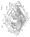
- Fig. 1 is a perspective view, with portions broken away for clarity, of a semiconductor device 30 of a preferred embodiment according to the present invention.
- Fig. 2 is a plan view showing a quarter of a power module 10 included in the semiconductor device 30. A portion shown in Fig. 2 is equivalent to a unit module 10a.
- the power module 10 of Fig. 1 includes four unit modules 10a to 10d.
- the power module 10 is fixed on a copper base plate 1.
- Main electrode terminals 32 (32a, 32b) and a control electrode terminal 33 are mounted upright on the upper surface of the power module 10.
- the power module 10 is located in the bottom of the semiconductor device 30, and is housed in a case 31.
- the case 31 may be an insert case or an outsert case.
- the "insert case” means a case to which the electrode terminals 32, 33 have been previously attached, and the “outsert case” means a case to which the electrode terminals 32, 33 are attached as the case 31 is mounted to the copper base plate 1.
- the case 31 has the shape of an open-bottomed box, the lower end thereof being soldered to the peripheral portion of the metal base plate 1. Resin is introduced into the case 31 through a hole 34 formed on the top of the case 31, and is heated to harden, whereby the power module 10 and the electrode terminals 32, 33 are sealed.
- Fig. 3 is a cross-sectional view taken along the line A-A of Fig. 2.
- the power module 10 includes a first composite substrate (laminate) 5 disposed on the upper major surface of the metal base plate 1.
- the first composite substrate 5 includes a ceramic insulating substrate 3 made principally of Al 2 O 3 or AlN, a copper pattern 4 deposited on the upper major surface of the ceramic insulating substrate 3, and a copper layer 2 deposited almost over the lower major surface of the ceramic insulating substrate 3.
- Fig. 4 shows only the first composite substrate 5 on the metal base plate 1 in plan view.
- the copper pattern 4 is roughly divided into four regions 4a to 4e.
- the broken line of Fig. 4 is a phantom line conceptually showing the boundary between the region 4a and the regions 4b to 4d.
- the region 4a is continuous with the regions 4b to 4d.
- the first region 4a is a strip-shaped region extending in a direction X parallel to the upper major surface of the metal base plate 1.
- the second regions 4b, 4c are of peninsular configuration extending from a side face of the first region 4a in a direction Y substantially perpendicular to the direction X.
- a slit 70 is formed between the second regions 4b and 4c. The slit 70 extends in the Y direction, and the deepest portion thereof reaches the side face of the first region 4a.
- the third region 4d extends from an end of the first region 4a in the Y direction.
- a slit 71 is formed between the third region 4d and the second region 4b.
- the fourth region 4e is provided in a position isolated from the first to third regions 4a to 4d.
- a second composite substrate 9 is provided on the upper major surface of the first region 4a (Fig. 4) of the conductive pattern 4 of the first composite substrate 5.
- the second composite substrate 9 includes a ceramic insulating substrate 7 made principally of Al 2 O 3 or AlN, a copper pattern 8 deposited almost over the upper major surface of the ceramic insulating substrate 7, and a copper layer 6 deposited almost over the lower major surface of the ceramic insulating substrate 7.
- the plan size of the second composite substrate 9 is smaller than that of the first composite substrate 5 and is generally equivalent to that of the first region 4a (Fig. 4) of the conductive pattern 4.
- Fig. 5 is a plan view of the second composite substrate 9.
- the copper layer 8 is a copper strip extending in the X direction.
- the copper layer 6 not shown in Fig. 5 on the lower major surface of the ceramic insulating substrate 7 is also a copper strip extending in the X direction.
- the thickness of the copper patterns 4, 8 and the copper layers 2, 6 is selected from the range of 0.1 to 0.5 mm, respectively.
- the spacing between the copper pattern 4 and the copper layer 2 and the spacing between the copper pattern 8 and the copper layer 6 are preferably selected from the range of 0.5 to 1.5 mm. This is achieved by selecting the thickness of the respective ceramic insulating substrates 3, 6 from the range of 0.5 to 1.5 mm.
- a plurality of power semiconductor chips 12 and a plurality of flywheel diode chips 11 are soldered onto the second regions 4b, 4c of the copper pattern.
- the power semiconductor chips 12 are IGBTs (insulated gate bipolar transistors) each of which has emitter and gate exposed on the upper major surface thereof and a collector exposed on the lower major surface thereof.
- Each of the flywheel diode chips 11 has a cathode exposed on the upper major surface thereof and an anode exposed on the lower major surface thereof.
- One power semiconductor chip 12 and two flywheel diode chips 11 make one set, and a plurality of sets of chips 12, 11 are spaced in the X direction.
- Aluminum wires 13 extending substantially in the Y direction are laid between the copper pattern 8 of the second composite substrate 9 and the upper major surface (cathode) of the flywheel diode chips 11, between the copper pattern 8 and the emitter on the upper major surface of the power semiconductor chips 12, and between the fourth region 4e of the copper pattern 4 and the gate on the upper major surface of the power semiconductor chips 12.
- the aluminum wires associated with the semiconductor chips 11, 12 illustrated on the upper side of Fig. 2 are not shown in Fig. 2.
- Fig. 6 is an equivalent circuit diagram of the unit module 10a of the present preferred embodiment having such wiring.
- an area 14a is defined in a (+X)-side end portion of the copper pattern 8.
- the main electrode terminal 32a of Fig. 1 is connected to the area 14a.
- An area 14b is defined in the third region 4d of the copper pattern 4.
- the main electrode terminal 32b of Fig. 1 is connected to the area 14b.
- the lower structure of the main electrode terminal 32b is not shown in Fig. 1.
- An area 14c is defined in a (+X)-side portion of the fourth region 4e of the copper pattern 4 of Fig. 2.
- the control electrode terminal 32a of Fig. 1 is connected electrically to the area 14c.
- the other unit modules 4b to 4d of Fig. 1 have the same structure as the unit module 4a.
- a positive voltage is applied to the main electrode terminal 32b of Fig. 1, and a negative voltage is applied to the main electrode terminal 32a.
- a control voltage which is positive to the main electrode terminal 32a is applied to the control electrode terminal 33. Then the power semiconductor chips 12 turn on. A current flow at this time will be described hereinafter.
- Fig. 7 is a plan view, with portions of the upper structure of Fig. 2 broken away.
- Fig. 8 shows a current flow of Fig. 1.
- the arrows 15 and 16 of Figs. 7 and 8 indicate the paths of input and output currents, respectively, when the power semiconductor chips 12 conduct in the forward direction.
- the input current flowing from the main electrode terminal 32b is directed from the area 14b of Fig. 2 to the third region 4d of the conductive pattern 4, and then reaches the first region 4a.
- the input current entering the first region 4a flows in the first region 4a in the (-X) direction. Since the copper layer 6 (Fig. 3) on the reverse side of the second composite substrate is soldered to the first region 4a, the input current flows in the copper layer 6 in the (-X) direction.
- the input current changes its direction to the (+Y) direction as it reaches the boundary between the first region 4a and the second regions 4b, 4c, to flow into the second regions 4b, 4c.
- the input current flowing in the second regions 4b, 4c in the (+Y) direction flows into the lower major surface or the collector of the power semiconductor chips 12.
- Such input current path is shown as the path 15.
- the output current flowing out of the emitter on the upper major surface of the power semiconductor chips 12 is directed through the aluminum wires 13 to the copper pattern 8. Since the aluminum wires 13 extend substantially in the Y direction, the output current is antiparallel to the input current flowing in the second regions 4b, 4c.
- the output current changes its direction to the (+X) direction as it reaches the copper pattern 8 through the aluminum wires 13.
- the output current flows to the area 14a in the (+X) direction, and then flows to the exterior from the area 14a through the main electrode terminal 32a.
- the direction of the input current flowing in the first region 4a of the copper pattern 4 is antiparallel to that of the output current flowing in the copper pattern 8. That is, the input current flows in the (-X) direction and the output current flows in the (+X) direction in these portions. This provides for a small inductance of the main current path in these portions.
- the copper pattern 8 is disposed just above the first region 4a, great effects to reduce the floating inductance are provided.
- the aluminum wires 13 and the second peninsular regions 4b, 4c enable the reduction in floating inductance by the antiparallel combination of "lines” (wires 13) and "planes" (regions 4b, 4c).
- the first region 4a of the copper pattern 4 and the copper pattern 8 enable the reduction in floating inductance by the antiparallel combination of a "plane” (copper pattern 8) and a "plane” (region 4a).
- the use of both combinations affords remarkable effects to reduce the floating inductance in the semiconductor device 30 of the present invention.
- the slit 70 is located between two pairs of semiconductor chips, and the slit 71 is located between the second region 4b and the third region 4d of the copper pattern 4.
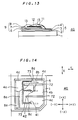
- Fig. 9 shows a structure wherein the slits 70, 71 are absent.
- a copper pattern 4m is of rectangular configuration, and the area 14b to be connected to the main electrode terminal 32b of Fig. 1 is defined in an end portion of the copper pattern 4m.
- Regions 12a represent positions in which the semiconductor chips 12 and the like are to be mounted.
- the current path 15 of the input current does not run just under the copper pattern 8 of the second composite substrate 9.
- the current path 15 runs in oblique directions.
- the semiconductor device of the present preferred embodiment of Fig. 2 having the slits 70, 71 is capable of forcing the input current path 15 to run in the (-X) direction (Fig. 7) and then to change its direction to the (+Y) direction so as to provide an L-shaped path. Furthermore, the input current path 15 runs adjacent the output current path 16, providing great effects to cancel the magnetic fields mutually.
- the semiconductor device 30 is fabricated, for example, in a manner to be described hereinafter.
- First prepared is the first composite substrate 5 including the insulating substrate 3, the copper pattern 4 deposited on the upper major surface of the insulating substrate 3, and the copper layer 2 deposited on the lower major surface of the insulating substrate 3. Also prepared is the second composite substrate 9 including the insulating substrate 7, the copper pattern 8 deposited on the upper major surface of the insulating substrate 7, and the copper layer 6 deposited on the lower major surface of the insulating substrate 7. The size of the second composite substrate 9 is determined in accordance with the size of the first region 4a of the copper pattern 4 of the first composite substrate 5.
- the first composite substrate 5 is joined to the upper major surface of the metal base plate 1 such that the copper layer 2 is positioned in face-to-face relation to the upper major surface of the metal base plate 1.
- the second composite substrate 9 is joined onto the first region 4a of the copper pattern 4 of the first composite substrate 5.
- the junction may be made by means of direct-connect process or activated metal process. Specifically, the junction is achieved by high-temperature brazing using hard solder or by using, as junction layers, copper oxide provided by heating the copper layers 2, 4, 6, 8 in an atmosphere of oxygen.
- Fig. 10 shows the power module after the junction.
- the metal base plate 1, the first laminate 5, and the second laminate 9 are joined together with junction layers 18, 17.
- the flywheel diode chips 11 and the power semiconductor chips 12 are soldered onto the second regions 4b, 4c of the copper pattern 4.
- the wires 13 are laid between the semiconductor chips 11, 12 and the copper patterns 8, 4e to bond the ends of the wires 13 to the semiconductor chips 11, 12 and the copper patterns 8, 4e.
- the power module provided in the foregoing manner is housed in the case 31 (Fig. 1). Almost simultaneously, the electrode terminals 32, 33 (Fig. 1) are joined to the corresponding areas 14a to 14d (Fig. 2).
- Resin is introduced into the case 31 through the hole 34 formed in the upper surface of the case 31, and is then heated to harden.
- the semiconductor chips 11, 12, the wires 13 and their vicinities may be protected with silicon gel or the like.
Landscapes
- Inverter Devices (AREA)
- Power Conversion In General (AREA)
- Thyristors (AREA)
- Electrodes Of Semiconductors (AREA)
Claims (20)
- Halbleitergerät zur Steuerung eines Eingangsstroms durch ein Halbleiterchip zur Bereitstellung eines Ausgangsstroms, enthaltend:(a) eine Metallbasisplatte (1) mit einer Hauptoberfläche;(b) ein erstes isolierendes Substrat (3), das auf der Hauptoberfläche der Metallbasisplatte angeordnet ist;(c) eine erste leitfähige Schicht (4), die auf dem ersten isolierenden Substrat vorgesehen ist und folgendes aufweist:(c-1) einen ersten Bereich (4a), zum Leiten des Eingangsstroms oder des Ausgangsstroms in einer ersten Richtung (X) parallel zu der genannten Hauptoberfläche, und(c-2) einen zweiten halbinselförmigen Bereich (4b, 4c), der mit dem ersten Bereich kontinuierlich verbunden ist und von ihm in einer zweiten Richtung (Y) weg steht, welche auf der genannten Hauptoberfläche von der genannten ersten Richtung (X) verschieden ist;(d) ein zweites isolierendes Substrat (7), das auf der ersten leitfähigen Schicht (4) mit Ausnahme mindestens eines Endabschnitts des genannten zweiten Bereichs (4b, 4c) vorgesehen ist;(e) eine zweite leitfähige Schicht (8), welche auf dem genannten zweiten isolierenden Substrat (7) vorgesehen ist und einen dritten Bereich (8a) zum Leiten des jeweils anderen der genannten Ströme in einer dritten Richtung antiparallel zu der genannten ersten Richtung aufweist, wobei der genannte dritte Bereich (8a) über dem ersten Bereich (4a) der ersten leitfähigen Schicht (4) liegt; und(f) mindestens ein Halbleiterchip (12), das auf dem zweiten Bereich (4b, 4c), oder der zweiten leitfähigen Schicht (8) vorgesehen ist und elektrisch mit dem zweiten Bereich (4b, 4c) und der genannten zweiten leitfähigen Schicht verbunden ist.
- Halbleitergerät nach Anspruch 1, bei welchem
(f-1) eine Mehrzahl von Halbleiterchips (12) auf dem genannten zweiten Bereich (4b, 4c) und in der genannten ersten Richtung beabstandet vorgesehen sind, und ein Schlitz (70) im wesentlichen parallel zu der genannten zweiten Richtung in dem genannten zweiten Bereich in einem Abschnitt vorgesehen ist, der der genannten Beabstandung entspricht. - Halbleitergerät nach Anspruch 2, weiter enthaltend:(g) eine erste Elektrode (32b), welche elektrisch mit einem Ende des ersten Bereichs (4a) verbunden ist; und(h) eine zweite Elektrode (32a), welche elektrisch mit einem Ende der genannten zweiten leitfähigen Schicht verbunden ist, das auf derselben Seite wie das genannte Ende des ersten Bereichs liegt.
- Halbleitergerät nach einem der vorhergehenden Ansprüche, weiter enthaltend:
(i) eine dritte leitfähige Schicht (2), die zwischen der Metallbasisplatte (1) und dem ersten isolierenden Substrat (3) vorgesehen ist. - Halbleitergerät nach einem der vorgehenden Ansprüche, bei welchem die jeweilige Dicke der ersten und zweiten leitfähigen Schichten (4, 8) im Bereich von 0,1 bis 0,5 mm gewählt ist.
- Halbleitergerät nach einem der Ansprüche 1 bis 4, bei welchem ein Abstand zwischen der ersten und zweiten leitfähigen Schicht (4, 8) im Bereich von 0,5 bis 1,5 mm gewählt ist.
- Halbleitergerät nach einem der vorhergehenden Ansprüche, bei welchem die ersten und zweiten leitfähigen Schichten (4, 8) im wesentlichen aus Kupfer hergestellt sind.
- Halbleitergerät nach einem der vorhergehenden Ansprüche, weiter enthaltend:
(g) mindestens einen Draht (13), der elektrisch jede Oberseite des genannten mindestens einen Halbleiterchips (12) und den zweiten Bereich (4b, 4c) oder die zweite leitfähige Schicht (8) verbindet, um den Eingangsstrom oder den Ausgangsstrom zu leiten, wobei sich der mindestens eine Draht im wesentlichen der zweiten Richtung erstreckt. - Halbleitergerät nach Anspruch 8, bei welchem das genannte zumindest eine, erste Halbleiterchip (12) folgendes enthält:(f-1) mindestens ein erstes Chip (12), das auf dem zweiten Bereich (4b, 4c) vorgesehen ist; und(f-2) mindestens ein zweites Chip (12), das auf der zweiten leitfähigen Schicht (8) vorgesehen ist; undwobei jeder zumindest eine Draht (13) folgendes enthält:(g-1) ein erstes Ende, das elektrisch mit einer der oberen Seiten des mindestens einen ersten Chips (12) verbunden ist; und(g-2) ein zweites Ende, das elektrisch mit einer Oberseite des mindestens einen zweiten Chips (12) verbunden ist.
- Halbleitergerät nach einem der vorhergehenden Ansprüche, bei welchem die genannte zweite leitfähige Schicht (8) weiter folgendes enthält:
(e-1) einen vierten halbinselförmigen Bereich (8b, 8c), der kontinuierlich mit dem dritten Bereich (8a) verbunden ist und in der zweiten Richtung (Y) wegsteht, um über dem zweiten Bereich (4b, 4c) mit Ausnahme eines Endabschnitts desselben zu liegen,bei welchem das zumindest eine Halbleiterchip (12) folgendes enthält:
(f-1) eine Mehrzahl von Halbleiterchips, die auf dem vierten halbinselförmigen Bereich vorgesehen sind und in der genannten dritten Richtung beabstandet sind, undwobei ein Schlitz (73) im wesentlichen parallel zu der genannten dritten Richtung in dem vierten halbinselförmigen Bereich in einem Abschnitt vorgesehen ist, welcher der genannten Beabstandung entspricht. - Verfahren zur Herstellung eines Halbleitergeräts zur Steuerung eines Eingangsstroms durch ein Halbleiterchip zur Bereitstellung eines Ausgangsstroms, wobei das Verfahren folgende Schritte umfaßt:(a) Bereitstellen eines Laminats (19), das ein erstes isolierendes Substrat (3), eine erste leitfähige Schicht (4), ein zweites isolierendes Substrat (7) und eine zweite leitfähige Schicht (8) enthält, welche in der angegebenen Reihenfolge miteinander verbunden sind, wobei die ersten und zweiten leitfähigen Schichten (4, 8) jeweils mindestens teilweise freiliegen;(b) Befestigen des genannten Laminats (19) auf einer Hauptoberfläche einer Metallbasisplatte (1); und(c) Befestigen eines Halbleiterchips (12) auf einer oberen freiliegenden Oberfläche der ersten oder zweiten leitfähigen Schicht (4, 8) des genannten Laminats, wobeidie erste leitfähige Schicht (4) einen ersten Bereich (4a) zum Leiten eines Eingangsstroms oder Ausgangsstroms in einer ersten Richtung (X) parallel zu der genannten Hauptoberfläche, sowie einen zweiten, halbinselförmigen Bereich (4b, 4c) enthält, der kontinuierlich mit dem ersten Bereich verbunden ist und von dem ersten Bereich auf der Hauptoberfläche in einer zweiten Richtung (Y) wegsteht, die von der ersten Richtung verschieden ist,das zweite isolierende Substrat (7) auf der ersten leitfähigen Schicht (4) mit Ausnahme mindestens eines Endabschnitts des genannten zweiten Bereichs (4b, 4c) vorgesehen ist, unddie zweite leitfähige Schicht (8) auf dem zweiten isolierenden Substrat (7) vorgesehen ist und einen Abschnitt zum Leiten des jeweils anderen der genannten Ströme in einer dritten Richtung antiparallel zu der genannten ersten Richtung (X), wobei der genannte Abschnitt über dem ersten Bereich (4a) der ersten leitfähigen Schicht (4) gelegen ist.
- Verfahren nach Anspruch 11, bei welchem der Schritt (a) die folgenden Schritte enthält:(a-1) Vorsehen des ersten isolierenden Substrats (3);(a-2) Selektives Erzeugen der genannten ersten leitfähigen Schicht (4) auf dem ersten isolierenden Substrat (3);(a-3) selektives Vorsehen des zweiten isolierenden Substrats (7) auf der ersten leitfähigen Schicht (4); und(a-4) Erzeugen der zweiten leitfähigen Schicht (8) auf dem zweiten isolierenden Substrat, wobei der Schritt (a-4) folgende Schritte umfaßt:(a-4-1) Vorsehen eines leitfähigen Streifens, der in Aufsicht kleiner als die erste leitfähige Schicht (4) ist; und(a-4-2) Befestigen des leitfähigen Streifens auf dem zweiten isolierenden Substrat (7), wobei die Länge des leitfähigen Streifens in die zweite Richtung (Y) weist, um die zweite leitfähige Schicht (8) zu bilden.
- Verfahren nach Anspruch 12, welches weiter folgende Schritte umfaßt:(d) Vorsehen einer ersten Elektrode (32b), um ein Ende der ersten leitfähigen Schicht (4) mit der ersten Elektrode zu verbinden; und(e) Vorsehen einer zweiten Elektrode (32a) zur elektrischen Verbindung eines auf derselben Seite wie das genannte Ende der ersten leitfähigen Schicht gelegenen Endes der zweiten leitfähigen Schicht (8) mit der zweiten Elektrode.
- Verfahren nach Anspruch 13, bei welchem der Schritt (a-2) folgenden Schritt enthält:
(a-2-1) Vorsehen einer Metallschicht mit einer Dicke, die im Bereich von 0,1 bis 0,5 mm gewählt ist, um die erste leitfähige Schicht (4) zu bilden, und bei welchem der Schritt (a-4-1) folgenden Schritt enthält:
(a-4-1-1) Vorsehen einer Metallschicht, welche eine Dicke aufweist, die im Bereich von 0,1 bis 0,5 mm gewählt ist, um den genannten leitfähigen Streifen zu bilden. - Verfahren nach Anspruch 12, 13 oder 14, bei welchem der Schritt (a-3) folgenden Schritt enthält:
(a-3-1) Befestigen der zweiten isolierenden Schicht (7) auf der ersten leitfähigen Schicht (4) derart, daß der Abstand zwischen der ersten und zweiten leitfähigen Schicht (4, 8) einen Wert im Bereich von 0,5 bis 1,5 mm hat. - Verfahren zur Herstellung eines Halbleitergeräts zur Steuerung eines Eingangsstroms durch ein Halbleiterchip zur Bereitstellung eines Ausgangsstroms, wobei das Verfahren folgende Schritte umfaßt:(a) Bereitstellen eines ersten Laminats (5), das ein erstes isolierendes Substrat (3) sowie erste und zweite leitfähige Schichten (2, 4) enthält, die auf der ersten bzw. zweiten Hauptoberfläche des ersten isolierenden Substrats (3) abgelagert sind, sowie eines zweiten Laminats (9), das ein zweites isolierendes Substrat (7) sowie dritte und vierte leitfähige Schichten (6, 8) enthält, welche auf der ersten bzw. zweiten Oberfläche des zweiten isolierenden Substrats (7) abgelagert sind;(b) Befestigen des ersten Laminats (5) auf einer Hauptoberfläche einer Metallbasisplatte (1) in solcher Weise, daß die erste leitfähige Schicht (2) flächig an der Hauptoberfläche der Metallbasisplatte anliegt;(c) Befestigen des zweiten Laminats (9) an dem ersten Laminat (5) in solcher Weise, daß die dritte leitfähige Schicht (6) flächig an der zweiten leitfähigen Schicht (4) anliegt und derart, daß ein Teil einer Hauptoberfläche der zweiten leitfähigen Schicht (4) freiliegt; und(d) Befestigen des genannten Halbleiterchips (12) an dem genannten Abschnitt der Hauptoberfläche der zweiten leitfähigen Schicht (4) oder auf der vierten leitfähigen Schicht (8),wobei die zweite leitfähige Schicht (4) einen ersten Bereich (4a) zum Leiten des Eingangsstroms oder des Ausgangsstroms in einer ersten Richtung (X) parallel zu der Hauptoberfläche der Metallbasisplatte (1), und einen zweiten, halbinselförmigen Bereich (4b, 4c) aufweist, der kontinuierlich mit dem ersten Bereich (4a) verbunden ist und in einer zweiten Richtung, die von der ersten Richtung verschieden ist, auf der Hauptoberfläche der Metallbasisplatte (1) wegsteht,wobei das zweite isolierende Substrat (7) auf der zweiten leitfähigen Schicht (4) mit Ausnahme mindestens eines Endabschnitts des genannten zweiten Bereichs (4b, 4c) vorgesehen ist, undwobei die vierte leitfähige Schicht (8) einen Abschnitt zum Leiten des anderen der genannten Ströme in einer dritten Richtung antiparallel zu der genannten ersten Richtung aufweist, der über dem ersten Bereich (4a) der zweiten leitfähigen Schicht (4) gelegen ist.
- Verfahren nach Anspruch 16, bei welchem der Schritt (a) folgenden Schritt enthält:
(a-1) Bereitstellen des zweiten Laminats (9) so, daß das zweite Laminat in Aufsicht kleiner als die zweite leitfähige Schicht (4) und von langgestreckter Gestalt ist, und
bei welchem der Schritt (b) folgenden Schritt umfaßt:
(b-1) Befestigen des zweiten Laminats (9) auf dem ersten Laminat (5), wobei die Länge des zweiten Laminats in die zweite Richtung (Y) weist. - Verfahren nach Anspruch 17, gekennzeichnet durch folgende Schritte:(d) elektrisches Verbinden einer ersten Elektrode (32b) mit einem ersten Ende der zweiten leitfähigen Schicht (4); und(e) elektrisches Verbinden einer zweiten Elektrode (32a) mit einem zweiten Ende der vierten leitfähigen Schicht (8), das auf derselben Seite wie das erste Ende der zweiten leitfähigen Schicht gelegen ist.
- Verfahren nach Anspruch 18, bei welchem der Schritt (a-1) folgende Schritte enthält:(a-1-1) Befestigen erster und zweiter metallischer Schichten, die jeweils eine Dicke im Bereich von 0,1 bis 0,5 mm haben, auf den ersten bzw. zweiten Hauptoberflächen des ersten isolierenden Substrats (3) zur Bildung der ersten und zweiten leitfähigen Schichten (2, 4) des ersten Laminats (5); und(a-1-2) Befestigen von dritten und vierten Metallschichten, die jeweils eine Dicke im Bereich 0,1 bis 0,5 mm haben, auf der ersten bzw. zweiten Hauptoberfläche des zweiten isolierenden Substrats (7) zur Bildung der dritten und vierten leitfähigen Schichten (6, 8) des zweiten Laminats.
- Verfahren nach Anspruch 19, bei welchem der Schritt (a-1) weiter folgende Schritte enthält:(a-1-3) Erzeugen des ersten Laminats (5) in solcher Weise, daß ein Abstand zwischen den ersten und zweiten leitfähigen Schichten (2, 4) einen Wert hat, der aus dem Bereich 0,5 bis 1,5 mm gewählt ist; und(a-1-4) Erzeugen des zweiten Laminats (9) in solcher Weise, daß ein Abstand zwischen der dritten und vierten leitfähigen Schicht (6, 8) aus dem Bereich von 0,5 bis 1,5 mm gewählten Wert hat.
Applications Claiming Priority (2)
| Application Number | Priority Date | Filing Date | Title |
|---|---|---|---|
| JP4193979A JP2725954B2 (ja) | 1992-07-21 | 1992-07-21 | 半導体装置およびその製造方法 |
| JP193979/92 | 1992-07-21 |
Publications (2)
| Publication Number | Publication Date |
|---|---|
| EP0585578A1 EP0585578A1 (de) | 1994-03-09 |
| EP0585578B1 true EP0585578B1 (de) | 1997-03-12 |
Family
ID=16316963
Family Applications (1)
| Application Number | Title | Priority Date | Filing Date |
|---|---|---|---|
| EP93111381A Expired - Lifetime EP0585578B1 (de) | 1992-07-21 | 1993-07-15 | Halbleiterbauelement mit reduzierter Schaltinduktanz und Verfahren zu seiner Herstellung |
Country Status (5)
| Country | Link |
|---|---|
| US (1) | US5424579A (de) |
| EP (1) | EP0585578B1 (de) |
| JP (1) | JP2725954B2 (de) |
| KR (1) | KR0120918B1 (de) |
| DE (1) | DE69308691T2 (de) |
Families Citing this family (40)
| Publication number | Priority date | Publication date | Assignee | Title |
|---|---|---|---|---|
| JP2988243B2 (ja) * | 1994-03-16 | 1999-12-13 | 株式会社日立製作所 | パワー混成集積回路装置 |
| DE69535775D1 (de) * | 1994-10-07 | 2008-08-07 | Hitachi Ltd | Halbleiteranordnung mit einer Mehrzahl von Halbleiterelementen |
| US5569957A (en) * | 1994-10-31 | 1996-10-29 | Harris Corporation | Low inductance conductor topography for MOSFET circuit |
| US6049126A (en) * | 1995-12-14 | 2000-04-11 | Nec Corporation | Semiconductor package and amplifier employing the same |
| JP3480771B2 (ja) * | 1995-12-20 | 2003-12-22 | 三菱電機株式会社 | 半導体装置 |
| JP3168901B2 (ja) * | 1996-02-22 | 2001-05-21 | 株式会社日立製作所 | パワー半導体モジュール |
| US6954368B1 (en) | 1996-07-22 | 2005-10-11 | HYDRO-QUéBEC | Low stray interconnection inductance power converting molecule for converting a DC voltage into an AC voltage, and a method therefor |
| US6078501A (en) * | 1997-12-22 | 2000-06-20 | Omnirel Llc | Power semiconductor module |
| US6069403A (en) * | 1998-10-06 | 2000-05-30 | Intersil Corporation | Power module with lowered inductance and reduced voltage overshoots |
| JP4475757B2 (ja) * | 2000-07-19 | 2010-06-09 | 京セラ株式会社 | インバータ制御モジュール |
| JP3635012B2 (ja) * | 2000-07-26 | 2005-03-30 | 京セラ株式会社 | インバータ制御モジュール |
| JP4475773B2 (ja) * | 2000-08-11 | 2010-06-09 | 京セラ株式会社 | インバータ制御モジュール |
| DE10107609A1 (de) * | 2001-02-17 | 2002-08-29 | Power One Ag Uster | Spannungsversorgungsmodul |
| ATE311017T1 (de) | 2001-09-28 | 2005-12-15 | Siemens Ag | Anordnung mit leistungshalbleiterbauelementen zur leistungssteuerung hoher ströme und anwendung der anordnung |
| JP2003258179A (ja) * | 2002-02-28 | 2003-09-12 | Sanyo Electric Co Ltd | 半導体装置およびその製造方法 |
| US6844621B2 (en) * | 2002-08-13 | 2005-01-18 | Fuji Electric Co., Ltd. | Semiconductor device and method of relaxing thermal stress |
| US7327024B2 (en) | 2004-11-24 | 2008-02-05 | General Electric Company | Power module, and phase leg assembly |
| JP2006253516A (ja) * | 2005-03-14 | 2006-09-21 | Hitachi Ltd | パワー半導体装置 |
| JP4810898B2 (ja) * | 2005-06-29 | 2011-11-09 | 富士電機株式会社 | 半導体装置 |
| JP4866143B2 (ja) * | 2006-05-15 | 2012-02-01 | 三菱電機株式会社 | 電力用半導体装置 |
| JP5144284B2 (ja) * | 2008-01-16 | 2013-02-13 | 本田技研工業株式会社 | 電力変換回路 |
| JP4666185B2 (ja) * | 2008-06-26 | 2011-04-06 | 三菱電機株式会社 | 半導体装置 |
| EP3633723B1 (de) * | 2009-05-14 | 2023-02-22 | Rohm Co., Ltd. | Halbleiterbauelement |
| JP5293473B2 (ja) * | 2009-07-16 | 2013-09-18 | 富士電機株式会社 | 半導体パワーモジュール |
| JP5477157B2 (ja) * | 2010-05-17 | 2014-04-23 | 富士電機株式会社 | 半導体装置 |
| US8622754B2 (en) * | 2011-07-31 | 2014-01-07 | General Electric Company | Flexible power connector |
| US9099930B2 (en) | 2012-06-22 | 2015-08-04 | General Electric Company | Power converter and method of assembling the same |
| US8942020B2 (en) | 2012-06-22 | 2015-01-27 | General Electric Company | Three-level phase leg for a power converter |
| WO2014014012A1 (ja) * | 2012-07-19 | 2014-01-23 | 三菱電機株式会社 | 電力用半導体モジュール |
| JP5704190B2 (ja) * | 2013-06-13 | 2015-04-22 | 富士電機株式会社 | 半導体パワーモジュール |
| JP6395530B2 (ja) | 2014-09-11 | 2018-09-26 | 三菱電機株式会社 | 半導体装置 |
| JP6305362B2 (ja) * | 2015-03-06 | 2018-04-04 | 三菱電機株式会社 | 電力用半導体モジュール |
| WO2016174908A1 (ja) * | 2015-04-28 | 2016-11-03 | 株式会社 村田製作所 | パワーモジュール |
| JP6485257B2 (ja) * | 2015-07-01 | 2019-03-20 | 富士電機株式会社 | 半導体装置及び半導体装置の製造方法 |
| DE102016112602A1 (de) * | 2016-07-08 | 2018-01-11 | Danfoss Silicon Power Gmbh | Niederinduktives Leistungsmoduldesign |
| JP6980625B2 (ja) * | 2018-09-18 | 2021-12-15 | 株式会社東芝 | 端子板及び半導体装置 |
| JP7233570B2 (ja) * | 2019-05-14 | 2023-03-06 | ヒタチ・エナジー・スウィツァーランド・アクチェンゲゼルシャフト | 低インダクタンスゲート交差部を有するパワー半導体モジュール |
| DE102022118268A1 (de) | 2022-07-21 | 2024-02-01 | Semikron Elektronik Gmbh & Co. Kg | Baugruppe mit einem Kunststoffformkörper und einer Mehrzahl von Lastanschlusselementen und Leistungshalbleitereinrichtung hiermit |
| DE102022207850A1 (de) | 2022-07-29 | 2024-02-01 | Vitesco Technologies Germany Gmbh | Leistungselektronikmodul und Inverter mit einem Leistungselektronikmodul |
| DE102024114912A1 (de) * | 2024-05-28 | 2025-12-04 | Semikron Danfoss Elektronik Gmbh & Co. Kg | Leistungshalbleitermodul und Verfahren zu dessen Herstellung |
Family Cites Families (6)
| Publication number | Priority date | Publication date | Assignee | Title |
|---|---|---|---|---|
| JPS62160558A (ja) * | 1986-01-09 | 1987-07-16 | Mitsubishi Electric Corp | 伝送制御手順実現ソフトウエアの機能検査方法 |
| US4907068A (en) * | 1987-01-21 | 1990-03-06 | Siemens Aktiengesellschaft | Semiconductor arrangement having at least one semiconductor body |
| EP0381849A1 (de) * | 1989-02-07 | 1990-08-16 | Asea Brown Boveri Ag | Schnelle Leistungshalbleiterschaltung |
| JP2780372B2 (ja) * | 1989-08-29 | 1998-07-30 | 株式会社日立製作所 | デイスク制御装置のキヤツシユ組込制御方法 |
| US5202578A (en) * | 1989-09-11 | 1993-04-13 | Kabushiki Kaisha Toshiba | Module-type semiconductor device of high power capacity |
| DE3937045A1 (de) * | 1989-11-07 | 1991-05-08 | Abb Ixys Semiconductor Gmbh | Leistungshalbleitermodul |
-
1992
- 1992-07-21 JP JP4193979A patent/JP2725954B2/ja not_active Expired - Lifetime
-
1993
- 1993-06-21 KR KR1019930011287A patent/KR0120918B1/ko not_active Expired - Fee Related
- 1993-07-02 US US08/084,957 patent/US5424579A/en not_active Expired - Lifetime
- 1993-07-15 EP EP93111381A patent/EP0585578B1/de not_active Expired - Lifetime
- 1993-07-15 DE DE69308691T patent/DE69308691T2/de not_active Expired - Lifetime
Also Published As
| Publication number | Publication date |
|---|---|
| JP2725954B2 (ja) | 1998-03-11 |
| DE69308691D1 (de) | 1997-04-17 |
| KR940003015A (ko) | 1994-02-19 |
| JPH0645509A (ja) | 1994-02-18 |
| US5424579A (en) | 1995-06-13 |
| KR0120918B1 (ko) | 1997-10-20 |
| DE69308691T2 (de) | 1997-06-19 |
| EP0585578A1 (de) | 1994-03-09 |
Similar Documents
| Publication | Publication Date | Title |
|---|---|---|
| EP0585578B1 (de) | Halbleiterbauelement mit reduzierter Schaltinduktanz und Verfahren zu seiner Herstellung | |
| US5767573A (en) | Semiconductor device | |
| US12046584B2 (en) | Semiconductor module | |
| EP0588094B1 (de) | Halbleiterverbundelement mit reduzierter interner Induktanz | |
| US5488256A (en) | Semiconductor device with interconnect substrates | |
| JP7428017B2 (ja) | 半導体モジュール | |
| US8461623B2 (en) | Power semiconductor module | |
| JP7428018B2 (ja) | 半導体モジュール | |
| JP4955077B2 (ja) | 半導体装置 | |
| US11398448B2 (en) | Semiconductor module | |
| JP3941266B2 (ja) | 半導体パワーモジュール | |
| JPH0525392B2 (de) | ||
| JP2002153079A (ja) | 半導体装置 | |
| JP3228839B2 (ja) | 電力用半導体装置 | |
| US7847316B2 (en) | Semiconductor device and its manufacture | |
| JP3220366B2 (ja) | 半導体装置 | |
| US6664629B2 (en) | Semiconductor device | |
| EP0527033B1 (de) | Halbleitermodul | |
| US12136603B2 (en) | Semiconductor arrangement comprising a semiconductor element, a substrate and bond connecting means | |
| JP3133544B2 (ja) | 混成集積回路 | |
| JP3525823B2 (ja) | 相補型igbtの実装構造 | |
| US4984051A (en) | Semiconductor device having directly connected source terminal | |
| JPH0451489Y2 (de) | ||
| US20240355713A1 (en) | Semiconductor device | |
| CN223872763U (zh) | 集成组件及电子设备 |
Legal Events
| Date | Code | Title | Description |
|---|---|---|---|
| PUAI | Public reference made under article 153(3) epc to a published international application that has entered the european phase |
Free format text: ORIGINAL CODE: 0009012 |
|
| AK | Designated contracting states |
Kind code of ref document: A1 Designated state(s): DE FR GB |
|
| 17P | Request for examination filed |
Effective date: 19940829 |
|
| 17Q | First examination report despatched |
Effective date: 19950822 |
|
| GRAG | Despatch of communication of intention to grant |
Free format text: ORIGINAL CODE: EPIDOS AGRA |
|
| GRAH | Despatch of communication of intention to grant a patent |
Free format text: ORIGINAL CODE: EPIDOS IGRA |
|
| GRAH | Despatch of communication of intention to grant a patent |
Free format text: ORIGINAL CODE: EPIDOS IGRA |
|
| GRAA | (expected) grant |
Free format text: ORIGINAL CODE: 0009210 |
|
| AK | Designated contracting states |
Kind code of ref document: B1 Designated state(s): DE FR GB |
|
| REF | Corresponds to: |
Ref document number: 69308691 Country of ref document: DE Date of ref document: 19970417 |
|
| ET | Fr: translation filed | ||
| PLBE | No opposition filed within time limit |
Free format text: ORIGINAL CODE: 0009261 |
|
| STAA | Information on the status of an ep patent application or granted ep patent |
Free format text: STATUS: NO OPPOSITION FILED WITHIN TIME LIMIT |
|
| 26N | No opposition filed | ||
| REG | Reference to a national code |
Ref country code: GB Ref legal event code: IF02 |
|
| REG | Reference to a national code |
Ref country code: GB Ref legal event code: 746 Effective date: 20020306 |
|
| REG | Reference to a national code |
Ref country code: FR Ref legal event code: D6 |
|
| PGFP | Annual fee paid to national office [announced via postgrant information from national office to epo] |
Ref country code: FR Payment date: 20110727 Year of fee payment: 19 |
|
| PGFP | Annual fee paid to national office [announced via postgrant information from national office to epo] |
Ref country code: GB Payment date: 20110713 Year of fee payment: 19 Ref country code: DE Payment date: 20110713 Year of fee payment: 19 |
|
| GBPC | Gb: european patent ceased through non-payment of renewal fee |
Effective date: 20120715 |
|
| REG | Reference to a national code |
Ref country code: FR Ref legal event code: ST Effective date: 20130329 |
|
| PG25 | Lapsed in a contracting state [announced via postgrant information from national office to epo] |
Ref country code: DE Free format text: LAPSE BECAUSE OF NON-PAYMENT OF DUE FEES Effective date: 20130201 Ref country code: GB Free format text: LAPSE BECAUSE OF NON-PAYMENT OF DUE FEES Effective date: 20120715 Ref country code: FR Free format text: LAPSE BECAUSE OF NON-PAYMENT OF DUE FEES Effective date: 20120731 |
|
| REG | Reference to a national code |
Ref country code: DE Ref legal event code: R119 Ref document number: 69308691 Country of ref document: DE Effective date: 20130201 |